
 Open Access Article
 This Open Access Article is licensed under a
 Creative Commons Attribution 3.0 Unported Licence
Giant negative magnetoresistance in Ni(quinoline-8-selenoate)2†
Nicholas
Black
a,
Tonouchi
Daiki
b,
Michio M.
Matsushita
*b,
J. Derek
Woollins
*a,
Kunio
Awaga
b and
Neil
Robertson
 *c
*c
aEaStCHEM School of Chemistry, University of St Andrews, St Andrews, Fife KY16 9ST, UK
bResearch Centre for Materials Sciences & Department of Chemistry, Nagoya University Furo-cho, Chikusa, Nagoya 464-8602, Japan
cEaStCHEM School of Chemistry University of Edinburgh, Edinburgh, EH9 3FJ, UK. E-mail: neil.robertson@ed.ac.uk
First published on 7th December 2017
Abstract
The magnetic, structural, conductivity and magnetoresistance properties of [Ni(quinoline-8-selenoate)2] ([Ni(qs)2]) have been studied. Despite the insolubility of the material necessitating its study as a powdered sample, a remarkably high conductivity has been measured. The conductivity is an order of magnitude greater than the thin-film processable thiol analogue previously reported and has been interpreted through the same space-charge limited conduction mechanism with charges injected from the electrodes. The introduction of selenium, results in a material with conductivity approaching metallic due to the enhanced interaction between adjacent molecules. Additionally, under an applied magnetic field, the material displays a negative magnetoresistance effect above 35% at 2 K. The effect can still be observed at 200 K and is interpreted in terms of a double-exchange mechanism.
Introduction
Molecular electronics, encompassing the use of small molecules or polymers for use as conductors and semiconductors, has seen an incredible expansion in research, both academically and industrially, over a relatively short period of time. While much of the early study has focussed on large area devices, photovoltaics and light-emitting devices for example, and on low-cost transistors there is a great scope for incorporating the appealing properties of molecular materials into novel application for electronic materials.1–3 Indeed, as the field has matured, the development of new devices utilising the intrinsic properties that molecules can offer is an exciting objective.Coinciding with these developments the field of spintronics, the utilisation and manipulation of electronic spin in order to carry information, has come into prominence.4–8 Beginning with the discovery of giant magnetoresistance (GMR) and with development throughout the 1980s it now underpins the magnetic data storage industry, giving rise to magnetic data reading and hybrid logic-storage devices.9,10 Investigation into electronic materials for spintronics and related fields, has yielded devices showing magnetoresistance,11 switching,12 memory effects13 and is aimed towards quantum information processing,14 and can be seen in inorganic, organic and single-molecule materials. It is therefore somewhat natural that the two fields should combine into the field of molecular spintronics.6,15,16
Molecular spintronics is still in the early stages of its development. Exploitation of spin in molecular systems demonstrates remarkable potential for merging the higher functionality of spintronics with the molecular design and processing advantages of molecular materials. The most common method of incorporating molecular materials utilises non-magnetic organic spacers between ferromagnetic materials in a spin valve.11,15,16 This approach is, however, hampered by difficult interface engineering.17–19 Magnetoresistance has also been observed in organic diode arrangements employing a thin film of molecular semiconductor, although the interpretation is still controversial and the sign of the effect changes with experimental conditions.20 A particularly appealing alternative is utilising the intrinsic GMR possible in a film of paramagnetic molecular materials. This approach has previously been used to generate negative MR up to 95% and relies upon a well-understood double-exchange mechanism, but has so far been limited to very few classes of molecule.21–23 ([TPP]Dicyano(phthalocyaninato)iron)2 was the first material of its type to be examined for the relationship between molecular magnetism and charge transport.23,24 A controllable giant negative magnetoresistance (GNMR) of up to 95% was achieved, using magnetic fields up to 15 Tesla. The benzo-TTF based molecule, bearing a nitronyl nitroxide radical group, ETBN, was discovered to demonstrate both conductivity and magnetism.25 The diselena analogue (ESBN) was the first example of the coexistence of both conductivity and magnetism based upon organic spins without the presence of inorganic magnetic ions, and a giant negative magnetoresistance effect of 70% was observed.26
Whereas the previously discussed examples have been studied as brittle single crystals, our observation of giant negative magnetoresistance in vapour processed thin films of [Nickel(quinoline-8-thiolate)2] ([Ni(qt)2]) opened up new avenues in the application and design of molecular materials for spintronic devices. [Ni(qt)2] is paramagnetic, with Ni(II) in a distorted octahedral geometry due to the formation of intermolecular S–N bonds orientated along the a-axis (Fig. 1a). Measurements revealed a drop in electrical resistance of greater than 60% in a magnetic field. This magnetoresistive effect was still discernible up to 200 K, albeit lower than 1%. The magnetic interactions are explained by the well-understood double exchange mechanism.27
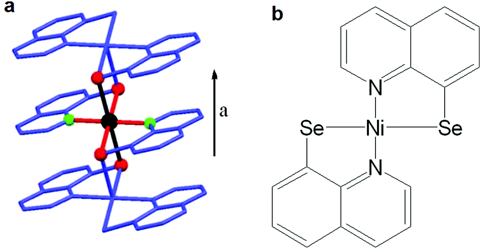 | ||
| Fig. 1 (a) Structure of [Ni(qt)2] and (b) new analogue [Ni(qs)2] substituting sulfur for selenium. | ||
In an effort to further explore and improve the intrinsic magnetoresistive effect observed in the [Ni(qt)2] material we have now studied the selenium analogue, Ni(quinolone-8-selenoate)2, [Ni(qs)2] (Fig. 1b). Sulfur and selenium have similar chemical properties however the larger selenium atom has more diffuse orbitals and so it was hypothesised that replacement of S with Se would increase orbital overlap and hence intermolecular interactions enhancing the previously observed effects.
Results and discussion
Synthesis and structure
Complexation of two-equivalents of quinoline-8-selenoate with Ni(OAc)2·4H2O in EtOH gave [Ni(qs)2] as an insoluble dark blue powder. The elemental analysis (C, H, N) satisfied the formula and the electron impact mass spectrum was in agreement with the [M]+ fragment with matching isotope pattern (Fig. S1, ESI†). It is noted that the material is exceptionally insoluble, hence the limitations on the analytical techniques used in characterisation. Both the microanalysis and the mass spectrum (ESI†) provide evidence that elemental composition is that of the desired product. In order to confirm the chain structure, as observed in the thiolato analogue, powder X-ray diffraction was carried out. The PXRD (Fig. S2, ESI†) was shown to have an amorphous component in addition to a crystalline component, observed as a bulging baseline with more defined peaks protruding from the baseline. The amorphous character may have arisen due to the polymeric nature of the chain, giving rise to an extremely insoluble material, with the rate at which the product precipitated from the reaction mixture resulting in the appearance of both the amorphous and crystalline character. Repeated measurements of samples prepared under various experimental conditions yielded the same result.Fig. 2(a) shows the magnetisation against magnetic field curve measured at 2.0 K, likely arising from a chain structure in analogue to [Ni(qt)2]. The metal has a formal oxidation state of +2 with a d8 electron count and would be diamagnetic in square planar geometry due to the crystal-field splitting (Fig. S3, ESI†). As the material is paramagnetic this provides a clear indication that the material synthesized is not in a square-planar geometry, but more likely the desired distorted octahedral geometry, as also seen for the sulfur analogue, since the octahedral crystal-field splitting gives two unpaired electrons for a d8 configuration (Fig. S3, ESI†). Fig. 2(b) shows the temperature dependence of the magnetic susceptibility for Ni(qs)2 measured at 1000 Oe. Fig. 2(b) inset shows the temperature dependence of the product of magnetic susceptibility and temperature (χT) for Ni(qs)2 measured at 1000 Oe. Above 40 K the χT value becomes almost constant after subtracting the temperature-independent components from χ − 1/T plot (Fig. S4, ESI†), and the value (Curie constant, 1.12) is consistent with the anticipated spin S = 1 with g = 2.12. The χT value increases with decreasing temperature below 30 K suggesting dominant ferromagnetic interactions, reaching 3.0 at 12 K. The sudden rise and then drop-off with decreasing temperature below 12 K suggests that antiferromagnetic ordering may exist between chains, or may be due to spin–orbit coupling, however without the single crystal structure reliable fitting of this is not possible. Overall however, paramagnetic S = 1 character of the Ni(II) centres, attributed to the formation of a chain structure, is apparent from the magnetic data.
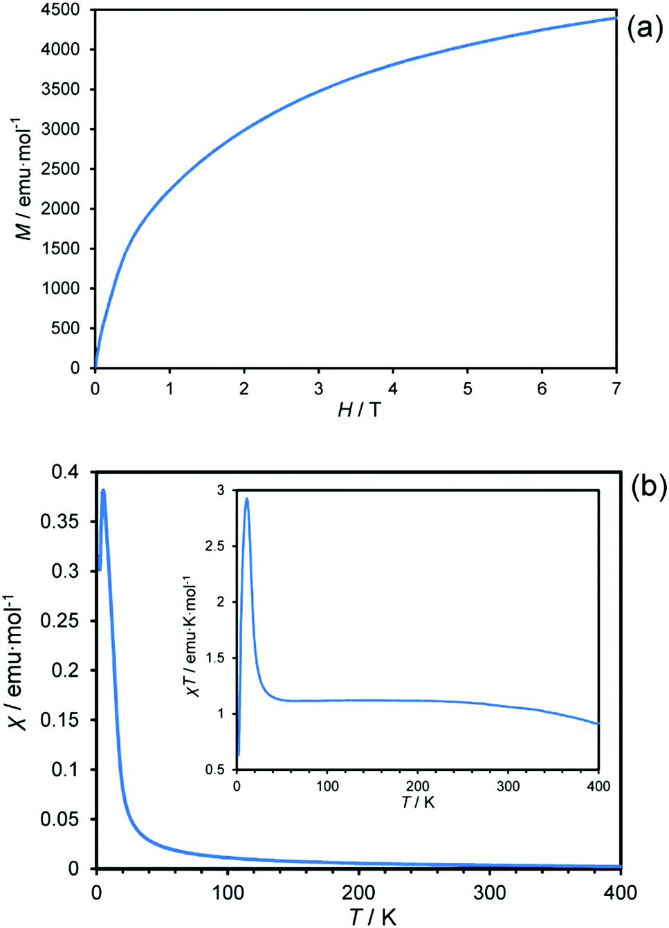 | ||
| Fig. 2 (a) Magnetisation against magnetic field curve of [Ni(qs)2] measured at 2.0 K. (b) Magnetic susceptibility of [Ni(qs)2] at varying temperature measured in a field of 1000 Oe and (inset). Temperature dependence of ChiT for [Ni(qs)2] measured at 1000 Oe. | ||
Conductivity and magnetoresistance
Due to the insolubility of the [Ni(qs)2] in all solvents and that attempts at sublimation resulted in decomposition, the material could not be processed into a thin-film which would have been the most desirable state for measurements. Also due to the insolubility of the material, single crystals could not be grown despite exhaustive attempts and so measurements were carried out on a powdered sample of [Ni(qs)2]. The powdered sample on an interdigitated electrode substrate was used to study the conductivity characteristics (Fig. S5, ESI†). As expected, the current versus voltage (I–V) characteristics of the sample showed strong non-linear behaviour (Fig. 3). With low bias voltage the observed currents are initially very low, increasing exponentially above a certain threshold voltage value (≈50 V at 2 K). Comparable results were measured previously for the [Ni(qt)2] analogue, however in the new [Ni(qs)2] material the observed currents are an order of magnitude greater than those previously observed for [Ni(qt)2].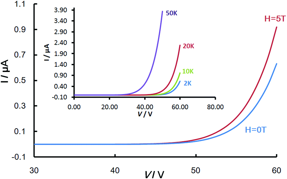 | ||
| Fig. 3 Magnetic field dependence of I–V at 2 K for [Ni(qs)2], the inset shows the non-linear I–V behaviour for the same device. | ||
From measurement of the resistivity temperature-dependence, an activation energy of Ea = 0.11–0.13 eV was calculated (Fig. S6, ESI†). This is very small and comparable to values measured for examples of single-component molecular conductors.30,31 The small activation energy suggests very strong intermolecular interaction, with a narrow band gap between occupied and unoccupied energy levels. This is in agreement with the visible spectrum measured by diffuse reflectance spectroscopy (Fig. S7, ESI†), which shows a broad absorption extending beyond the visible into the near-IR. Although an increase in conductivity was expected due to the enhanced interaction caused by the introduction of selenium, it is remarkable that the conductivity is so high in a powder sample where the effect of grain boundaries will likely be significant. A space-charge-limited conduction (SCLC) mechanism with carriers injected from the electrodes can be used to interpret the non-linear behaviour, as is the case in some other previously reported molecular examples.28,29 It is expected that, as is the case for [Ni(qt)2], the material possesses strong electron-donor property and that the injected carriers are holes and this is consistent with the measured electrochemical behaviour (Fig. S8, ESI†). Above the threshold voltage, the I–V behaviour can be modelled by an exponential law (I ∝ Vm+1) with m ranging from 4 to 18 at 200 and 2 K respectively, confirming that the current is dominated by a trapped-charge-limited conduction (TCLC) regime within the (SCLC) mechanism (Fig. S9, ESI†). In these conditions, the current is due to the bulk properties of the compound rather than the contact effects.
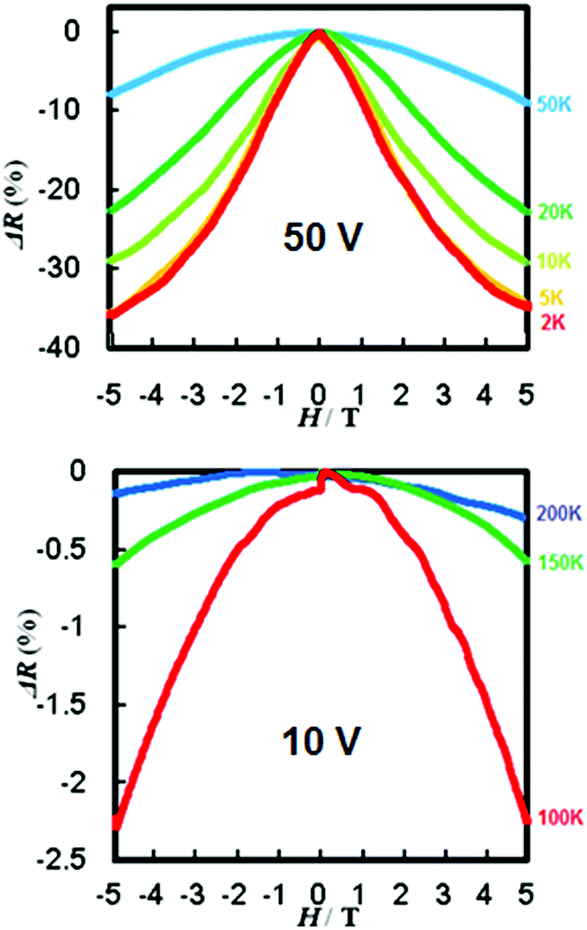
The same devices were also used to measure the magnetoresistance effect. A constant bias was applied and the magnetic field modified between −5 and 5 T. In order to ensure that each measurement of the current was made over a suitable region of the non-linear region an appropriate bias was selected for each temperature at which a measurement was made.
The experiment was setup with the magnetic field parallel to the current direction in order to avoid the appearance of Lorentz force. The observed giant negative magnetoresistance effect of [Ni(qs)2] is illustrated in Fig. 4. The magnetic field dependence of resistance of the [Ni(qs)2] complex reported as a percentage (R − R0T)/R0T, where R and R0T are the resistance with and without applied magnetic field, respectively. At 2 K the resistance decreases by more than 35%. This effect is still apparent (8%) at 50 K and still observable at 200 K although it has decreased below 0.5%. This is lower than that observed for the previous thiol analogue, however this may be partially explained by the measurements being made on a powder sample as opposed to ordered single crystals or evaporated multicrystalline thin-film.
 | ||
| Fig. 4 Magnetic field dependence of resistance of [Ni(qs)2] at various temperatures. | ||
Calculations and discussion
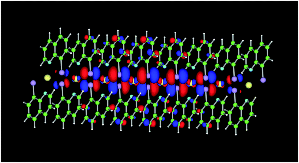
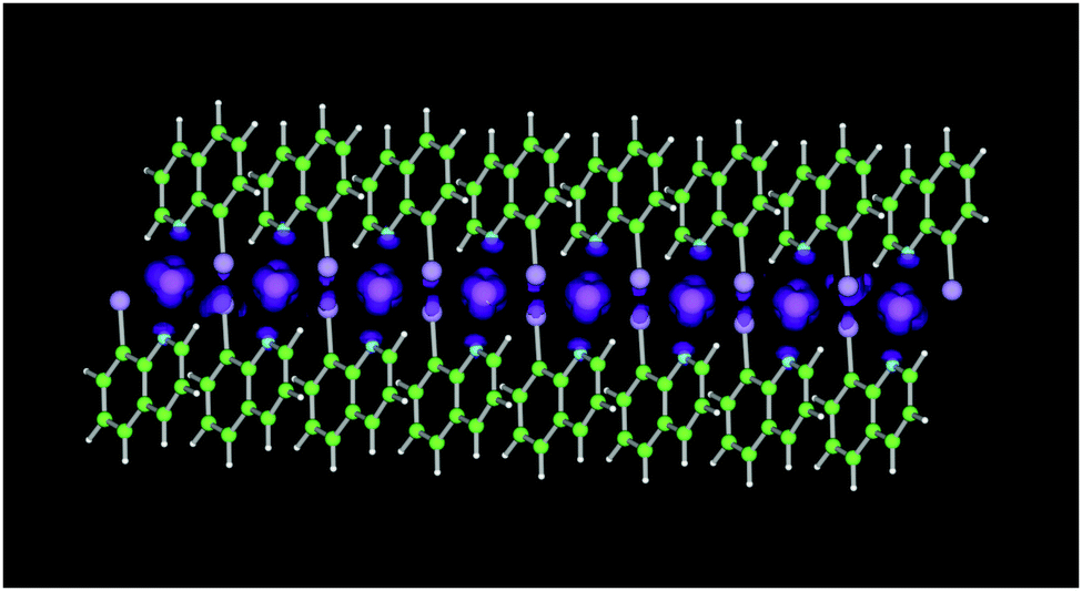
As the single crystal structure of the molecule is unknown, the structure had to first be modelled. From the empirical observations, it is likely that [Ni(qs)2] has the same general chain structure as the thiolato analogue. Using the structure of [Ni(qt)2] as the base and substituting the sulfur atoms for selenium the structure of a trimer was optimised. Calculations at the unrestricted B3LYP/DZVP level of theory were performed on an 8-mer of the chain, with the length chosen to approximate the spin correlation length at low temperature. The 8-mer was constructed using the geometry of the central molecule of the optimised trimer. The optimised structure reveals a relatively short distance between the selenium atoms of adjacent molecules, 3.51 Å, well within the sum of the van der Waals radii of two selenium atoms. It is likely that this interaction between the bridging atoms results in the great decrease in solubility of the material over the thio-analogue. The greatly enhanced conductivity of [Ni(qs)2], when compared to the previously reported [Ni(qt)2], analogue is also attributed to this interaction.Fig. 5 shows the calculated fully occupied HOMO which possesses predominantly ligand character. The HOMO is based largely upon the selenium atoms of the ligand and the positions on the ring ortho and para to the selenium, with some additional character on the other positions of the rings and the central Ni atoms. This is similar to what was previously calculated for [Ni(qt)2].
 | ||
| Fig. 5 Calculated HOMO of an 8-mer chain of [Ni(qs)2]. | ||
The calculated spin density is shown in Fig. 6 which, as anticipated, is predominantly located around the Ni(II) centre but with some character also on the ligand. This electronic structure resembles that of the thiolato analogue and is consistent with what would be expected for a system which follows the double exchange mechanism. As is the case for observations in nitronyl nitroxide-tetrathiafulvalene radicals, and the thiolato analogue, unpaired spins give rise to a Singly-Occupied Molecular Orbital (SOMO) of lower energy than the HOMO as necessitated by the double exchange mechanism. As shown in the density of states plot (Fig. S10, ESI†), contribution of the SOMOs of Ni(II) ions are found in the lower energy level (α − β), and the large energy differences (>0.5 eV) between α and β spins (spin-polarization) at the HOMO band is caused by the low-lying SOMOs. Hole transport via the HOMO orbitals based on the ligands is facilitated by the hole doping of the HOMO band at high applied electric field. The HOMO electrons on the ligand couple with the localized SOMO spins of the molecular unit which are aligned by an applied magnetic field. This results in the alignment of the spins of the HOMO electrons between neighbouring molecular units. As favourable spin alignment is maintained upon hole transfer this instigates hole hopping with reduced scattering. Due to co-location on a small molecular unit, the coupling between the HOMO and the SOMO spins is strong and consistent with the magnetoresistance effect persisting to high temperatures.
 | ||
| Fig. 6 Calculated spin density of an 8-mer chain of [Ni(qs)2]. | ||
Conclusion
In conclusion, the magnetic, structural, conductivity and magnetoresistance properties of [Ni(quinoline-8-selenoate)2] ([Ni(qs)2]) have been studied and the material shows a remarkably high conductivity for a single-component molecular material. As was anticipated, the introduction of selenium results in a great enhancement of the interaction between adjacent molecules and gives a pronounced improvement in conductivity over the thiolato analogue. Inevitably, this strong interaction also results in a reduction in the solubility of the material necessitating all measurements be carried out on a powder sample of the material. The conductivity is an order of magnitude greater than the previously reported, thin-film processable thiol analogue and has been interpreted through a space-charge limited conduction mechanism. [Ni(qs)2] also displays an intrinsic magnetoresistance effect; under an applied magnetic field the material displays a reduction in resistance of greater than 35% at 2 K. By analogy with the thiol analogue and earlier studies on TTF-derivatives, the effect may be attributed to a double-exchange mechanism and is still observable at 200 K. Adding to a family of molecular magnetoresistive materials with only very few examples, [Ni(qs)2] provides further evidence of the importance of strong intermolecular interactions for the development of functional materials.Experimental
All chemicals were purchased from Sigma Aldrich and used without further purification.General procedure for the synthesis of [Ni(qs)2]
Under an atmosphere of nitrogen diquinonyl-diselenide (0.25 g, 0.60 mmol) was dissolved in HCl (6 M, 5 mL) and degassed ethanol (15 mL). Hypophosphorus acid (50% aq., 2 mL) was added and the mixture stirred at 70 °C for 15 minutes. The solution was allowed to cool, before addition of a saturated solution of sodium acetate (7 mL) was added, followed immediately by a solution of Ni(CH3COO)2·4H2O (0.15 g, 0.60 mmol) in degassed water (3 mL) with vigorous stirring. The mixture was stirred for 10 minutes and the precipitate collected by filtration. The solid was washed with water, ethanol, ether and DCM to yield the pure product (0.24 g, 51 mmol, 85%). MS-EI+: m/z [M+] 473.9. Anal. calcd for C18H12NiN2Se2: C, 45.72; H, 2.56; N, 5.92. Found: C, 45.66; H, 2.50; N, 6.00.Magnetic and optical measurements
Magnetic susceptibility measurements were performed on powder samples from 1.8 to 300 K using a Quantum Design MPMS-XL SQUID Magnetometer with MPMS MultiVu Application software to process the data. The magnetic field used was 1 T. Diamagnetic corrections were applied to the observed paramagnetic susceptibilities by using Pascal's constants. Diffuse Reflectance measurements were recorded on powdered samples dispersed in BaSO4 using a integrating sphere attachment on a Jasco V-570 UV/Vis/NIR spectrophotometer.Conductivity measurements
Conductivity data were taken on powdered [Ni(qs)2] sample deposited on an interdigitated Pt electrode with a line width of 2 μm and gap of 2 μm in 2 × 2 mm area, corresponding to a 2 μm gap and 2000 mm long electrode, fabricated on a quartz glass substrate. The substrate with the sample was then attached on a hand-made probe and the electrodes were connected to with gold wires with gold paste, and the probe was introduced into the Quantum Design MPMS-XL cryostat with MPMS MultiVu Application software to control temperature from 2 to 300 K and magnetic field from 0 to ±5 T. Voltage-applying current measurement was carried out with Advantest R6245 Sourcemeter controlled with an original software.Computational
Theoretical calculation on an 8-mer of [Ni(qs)2] was carried out on UB3LYP/TZVP level with Gaussian09 program package. Since the 3-dimensional crystal structure of [Ni(qs)2] has not been solved, the structure of 8-mer was prepared based on an optimized structure of 3-mer: the structure of the central monomer in the optimized 3-mer was replicated 8 times and arranged to have the similar chain structure to [Ni(qt)2]. The Ni–Se distance was also set to the same to that in the optimised structure of [Ni(qs)2] 3-mer.Conflicts of interest
There are no conflicts of interest to declare.Acknowledgements
We thank the University of St Andrews, the Leverhulme Trust (International Network Grant IN-2012-094) and the JSPS Core-to Core Program, A. Advanced Research Networks for support.References
- A. C. Arias, J. D. MacKenzie, I. McCulloch, J. Rivnay and A. Salleo, Chem. Rev., 2010, 110, 3 CrossRef CAS PubMed.
- L. Sun, Y. A. Diaz-Fernandez, T. A. Gschneidtner, F. Westerlund., S. Lara-Avila and K. Moth-Poulsen, Chem. Soc. Rev., 2014, 43, 7378 RSC.
- J. P. Bergfield and M. A. Ratner, Phys. Status Solidi B, 2013, 250, 2249 CrossRef CAS.
- S. Sanvito, Chem. Soc. Rev., 2011, 40, 3336 RSC.
- T. D. Nguyen, E. Ehrenfreund and Z. V. Vardeny, Science, 2012, 337, 204 CrossRef CAS PubMed.
- S. D. Jiang, K. Goss, C. Cervetti and L. Bogani, Sci. China, 2012, 55, 867 CrossRef CAS.
- P. P. Freitas, F. A. Cardosa, V. C. Martins, S. A. M. Martins, J. Loureiro, J. Amaral, R. C. Chaves, S. Cardosa, L. P. Fonseca, A. M. Sebastião, M. Pannetier-Lecoeur and C. Fermon, Lab Chip, 2012, 12, 546 RSC.
- G. Li, S. Sun, R. J. Wilson, R. L. White, N. Pourmand and S. X. Wang, Sens. Actuators, A, 2006, 126, 98 CrossRef CAS PubMed.
- M. N. Baibich, J. M. Broto, A. Fert, F. Nguyen Van Dau, F. Petroff, P. Eitenne, G. Creuset, A. Friederich and J. Chazelas, Phys. Rev. Lett., 1988, 61, 2472 CrossRef CAS PubMed.
- D. D. Awschalom and M. E. Flatté, Nat. Phys., 2007, 3, 157 CrossRef.
- Z. H. Xiong, D. Wu, Z. V. Vardeny and J. Shi, Nature, 2004, 427, 821 CrossRef CAS PubMed.
- A. Rotaru, I. A. Curalskiy, G. Molnar, L. Salmon, P. Dermont and A. Bousseksou, Chem. Commun., 2012, 48, 4163 RSC.
- J. Lee, E. Lee, S. Kim, G. Sook Bang, D. A. Schultz, R. D. Schmidt, M. D. E. Forbes and H. Lee, Angew. Chem., Int. Ed., 2011, 50, 4414 CrossRef CAS PubMed.
- L. Bogani and W. Wernsdorfer, Nat. Mater., 2008, 7, 179 CrossRef CAS PubMed.
- J. W. Yoo, H. W. Jang, V. N. Prigodin, C. Kao, C. B. Eom and A. J. Epstein, Phys. Rev. B: Condens. Matter Mater. Phys., 2009, 80, 205207 CrossRef.
- J. W. Yoo, C. Y. Chen, H. W. Jang, C. W. Bark, V. N. Prigodin, C. B. Eom and A. J. Epstein, Nat. Mater., 2010, 9, 638 CrossRef CAS PubMed.
- P. Ruden, Nat. Mater., 2001, 10, 8 CrossRef PubMed.
- D. Sun, L. Yin, C. Sun, H. Guo, Z. Gai, X. G. Zhang, T. Z. Ward, Z. Cheng and J. Shen, Phys. Rev. Lett., 2010, 104, 236602 CrossRef PubMed.
- L. Schulz, L. Nuccio, M. Willis, P. Desai, P. Shayka, T. Kreouzis, V. K. Malik, C. Bernhard, F. L. Pratt, N. A. Morley, A. Suter, G. J. Niuewenhuys, T. Prokscha, E. Morenzoni, W. P. Gillin and A. J. Drew, Nat. Mater., 2011, 10, 39 CrossRef CAS PubMed.
- T. L. Francis, Ö. Mermer, G. Veeraraghaven and M. Wohlgenannt, New J. Phys., 2004, 6, 185 CrossRef.
- T. Sugawara, H. Komatsu and K. Suzuki, Chem. Soc. Rev., 2011, 40, 3105 RSC.
- D. Ethelbhert, C. Yu, M. Matsuda, H. Tajima, A. Kikuchi, T. Taketsugu, N. Hanasaki, T. Naito and T. Inabe, J. Mater. Chem., 2009, 19, 718 RSC.
- D. Ethelbhert, C. Yu, M. Matsuda, H. Tajima, T. Naito and T. Inabe, Dalton Trans., 2011, 40, 2283 RSC.
- N. Hanasaki, M. Matsuda, H. Tajima, E. Ohmichi, T. Osada, T. Naito and T. Inabe, J. Phys. Soc. Jpn., 2006, 75, 033703 CrossRef.
- J. Nakazaki, Y. Ishikawa, A. Izuoka, T. Sugawara and Y. Kawada, Chem. Phys. Lett., 2000, 319, 385 CrossRef CAS.
- M. M. Matsushita, H. Kawakami, M. Ogata and T. Sugawara, Phys. Rev. B: Condens. Matter Mater. Phys., 2008, 77, 195208 CrossRef.
- L. Pilia, M. Serri, M. M. Matsushita, K. Awaga, S. Heutz and N. Robertson, Adv. Funct. Mater., 2014, 24, 2383 CrossRef CAS.
- K. C. Kao and W. Hwang, Electrical Transport in Solids, Pergamon Press, Oxford, 1981 Search PubMed.
- P. E. Burrows, Z. Shen, D. M. McCarty, S. R. Forrest, J. A. Cronin and M. E. Thompson, J. Appl. Phys., 1996, 79, 7991 CrossRef CAS.
- E. Allwright, G. Silber, J. Crain, M. M. Matsushita, K. Awaga and N. Robertson, Dalton Trans., 2016, 45, 9363 RSC.
- D. Belo, H. Alves, E. B. Lopes, M. T. Duarte, V. Gama, R. T. Henriques, M. Almeida, A. Perez-Benltez, C. Rovira and J. Veciana, Chem. – Eur. J., 2001, 7, 511 CrossRef CAS.
Footnote |
| † Electronic supplementary information (ESI) available: Fig. S1: Mass spectrum of [Ni(qs)2]; Fig. S2: PXRD obtained for [Ni(qs)2]; Fig. S3: Square-planar and octahedral crystal-field splitting; Fig. S4: Magnetic susceptibility plots; Fig. S5: Powdered sample of [Ni(qs)2] on an interdigitated circuit; Fig. S6: T-Dependence of resistivity; Fig. S7: Diffuse reflectance of [Ni(qs)2]; Fig. S8: Cyclic voltammogram of solid [Ni(qs)2]; Fig. S9: log–log plots of I–V characteristics; Fig. S10: Calculated density of states plot for Ni(qs)2. See DOI: 10.1039/c7cp06273g |
| This journal is © the Owner Societies 2018 |