
 Open Access Article
 This Open Access Article is licensed under a Creative Commons Attribution-Non Commercial 3.0 Unported Licence
Characterization of a 4-inch GaN wafer by X-ray diffraction topography
Jaemyung
Kim
ab,
Okkyun
Seo
 abc,
Chulho
Song†
b,
Yanna
Chen
bc,
Satoshi
Hiroi
bc,
Yoshihiro
Irokawa
a,
Toshihide
Nabatame
a,
Yasuo
Koide
a and
Osami
Sakata
*abc
abc,
Chulho
Song†
b,
Yanna
Chen
bc,
Satoshi
Hiroi
bc,
Yoshihiro
Irokawa
a,
Toshihide
Nabatame
a,
Yasuo
Koide
a and
Osami
Sakata
*abc
aCenter for GaN Characterization, Research Network and Facility Services Division (RNFS), National Institute for Materials Science (NIMS), Tsukuba, Ibaraki, 305-0047 Japan. E-mail: SAKATA.Osami@nims.go.jp
bSynchrotron X-ray Station at SPring-8, RNFS, NIMS, Kouto, Sayo, Hyogo, 679-5148 Japan
cSynchrotron X-ray Group, Research Center for Advanced Measurement and Characterization, NIMS, Kouto, Sayo, Hyogo, 679-5148 Japan
First published on 16th November 2018
Abstract
We have investigated the crystal quality of a 4-inch GaN wafer by X-ray diffraction topography. GaN (11![[2 with combining macron]](https://www.rsc.org/images/entities/char_0032_0304.gif) 4) diffraction images at various incident angles were obtained to determine the image of maximum intensity and full-width at half-maximum (FWHM). The images reconstructed from the maximum intensity at each detector pixel position indicated that the inhomogeneous crystal quality of the wafer originated from seed crystals during wafer manufacturing. The evaluated FWHM distribution tended to increase and become broader from the center to the edge of the wafer. The q-vector components evaluated from the two rocking-curve images at different azimuthal angles combined with the rotation matrix revealed that the overall lattice planes bowed towards the diagonal direction. A histogram on the tilting angle of the wafer showed that the most frequently observed angle was about 0.03°. We expect that our findings could be applied to wafer quality estimation.
4) diffraction images at various incident angles were obtained to determine the image of maximum intensity and full-width at half-maximum (FWHM). The images reconstructed from the maximum intensity at each detector pixel position indicated that the inhomogeneous crystal quality of the wafer originated from seed crystals during wafer manufacturing. The evaluated FWHM distribution tended to increase and become broader from the center to the edge of the wafer. The q-vector components evaluated from the two rocking-curve images at different azimuthal angles combined with the rotation matrix revealed that the overall lattice planes bowed towards the diagonal direction. A histogram on the tilting angle of the wafer showed that the most frequently observed angle was about 0.03°. We expect that our findings could be applied to wafer quality estimation.
1 Introduction
Growing a high-quality large-sized GaN crystal is becoming important because of its wide engineering applications in optoelectronics1,2 and power devices.3,4 Not only the growth technique but also techniques to determine quality is in demand as the wafer size increases. A laser-based curvature measurement system has been used to examine the bending of the wafer.5 However, this method does not provide details of the crystal structure of the wafer but rather those along the surface normal direction. One conventional method to determine crystal quality is to use X-ray diffraction. To describe the crystallinity of wafers qualitatively, X-ray rocking curve measurements are performed at several points on the wafer.6–8 Although these rocking curve measurements have been performed, so far, they only yield details of the local structure at some wafer points. Therefore, to obtain details of the whole wafer, other imaging techniques are required such as X-ray diffraction topography.9–13 However, the imaging technique based on the Berg–Barrett method only provides the diffracted X-ray intensity without the orientation details. To solve this issue, rocking curve imaging techniques have been proposed.14–16 This method is suitable for understanding the one-directional orientation of the local structure. Rocking-curve imaging combined with the two rotation matrix operation that has been recently developed has yielded the q-vector components of the GaN (114) lattice planes and the lattice plane tilting of the wafer.17
Here, we propose a method to evaluate the crystal quality using X-ray diffraction topography of the wafer. We discuss the crystallinity and homogeneity of a 4-inch GaN wafer through FWHM distributions as a function of the wafer radius. In addition, we evaluate the q-vector components of GaN 114 by rotation matrix operations to understand the lattice tilting directions and distributions of the 4-inch wafer.
2 Experimental details and results
GaN seed crystals were grown by a conventional hydride vapour phase epitaxy (HVPE) method. After the growth is terminated, one side is polished so as to determine the crystal quality. The sample investigated was a 4-inch wafer. The X-ray diffraction topography was performed at BL20B2, SPring-8, Japan, which provided a large monochromatic beam [Fig. 1(a)]. The X-ray wavelength of 1.284 Å was selected using a Si (111) double crystal monochromator. GaN (114) lattice planes were chosen for the purpose of shining X-rays at a grazing incident. The incident angle was set to 0.58° with respect to the sample surface, which satisfied the GaN 114 Bragg conditions. The corresponding 2θB angle was about 79.3°. To irradiate monochromatic X-rays onto the whole wafer, the beam size for the incident X-rays was adjusted to 130 mm (h) × 10 mm (v) and fully covers the whole wafer under the grazing incident angle conditions. A flat-panel detector (FPD) was mounted almost parallel to the incident X-ray beam. The pixel size of the FPD is 50 × 50 μm2, and the distance from the wafer center to the detector center is 50 cm. By changing the X-ray incident angle θ0, we found that the image was partially diffracted from the wafer. We checked the upper and lower limits of θ0 for the rocking curve at every point of the wafer. The rocking angle (±0.2°) was incremented to 10 arcsec, small enough to describe the rocking curves at every point of the wafer. The X-ray exposure time was set to 20 s for each exposure. Fig. 1(b) shows the partial-diffracted GaN images at various incident angles. Because the wafer bends, only a partially diffracted image was obtained.
 | ||
| Fig. 1 (a) Schematic view of the experimental configuration. The monochromatic X-rays were selected using a Si (111) monochromator, and then the GaN (0001) surface was exposed with an incident angle of 0.58°. The 2θB angle was adjusted to 79.3°, which satisfied the GaN 114 diffraction. (b) Partially diffracted wafer images at various incident angles θ0 were obtained due to the wafer curvature. | ||
The conventional technique to obtain the X-ray diffraction topography images is using a plot and selecting the most intense value in the range of rotation angles at the respective pixel positions of the fixed detector. An image reconstructed by this technique is shown in Fig. 2(a). Fig. 2(b) is the high-magnification image of the Fig. 2(a) center. The intensity difference in Fig. 2(a) between the left and right region is due to the low incident angle variations at a fixed incident photon flux. The number of photons per unit area at low angles is proportional to θB, which is sensitive to the incident angle and bending angle.
 | ||
| Fig. 2 (a) Reconstructed image using maximum intensity at each FPD pixel position. (b) High magnification image of GaN. Regions of strong diffraction intensity (red) and low diffraction intensity (blue) are observed. The overall change in intensity from left to right stems from the different X-ray photons at different incident angles. (c) and (d) FWHM mapping images of the 4-inch GaN wafer; red areas with low crystallinity appear from the GaN seed crystals. | ||
We evaluated the FWHM to check the domain size of the wafer [Fig. 2(c) and (d), size is enlarged]. The color bars indicate FWHM values in units of °. The blue areas have low values implying highly oriented crystalline domains. The red areas show large mosaicity of the GaN wafer. The FWHM images show that the domains stemming from the seed crystals have non-uniform sizes but their values are very low and narrow. According to a report on GaN dislocation, the dislocation density was estimated by counting the number of black spots in the lines of the image used for density calculation.6 However, it is not clear from the image whether the black spots and lines are real dislocations. The best way to observe dislocations is to use transmission electron microscopy techniques at atomic resolutions18 or the recently developed two-photon excitation photoluminescence technique.19 Without these techniques, it is hard to evaluate the dislocation density. Even though X-ray rocking curves are used to describe the mosaicity of the GaN domains, obtaining the dislocation density through this method is difficult because many factors affect the diffraction profile.
To examine the FWHM uniformity of the wafer, we evaluated histograms by changing the distance from the wafer center to the edge. The distance r was varied from 5 to 45 mm at 5 mm increments with a constant wall thickness of 5 mm as illustrated in the scheme in Fig. 3. The normalized FWHM histogram was obtained as a function of r [Fig. 3(a)]. In the center of the wafer, the FWHM distribution has two peaks at 0.0067° (24 arcsec) and 0.0092° (33 arcsec). The origin of this peak splitting is not clear in this instance; however, these two values are reasonable when compared with those in other previous reports.6,20,21Fig. 3(b) shows the FWHM probability as a function of the radius r normalized by the maximum value at each FWHM angle. As the radius increases from the center, the first peak around 0.0067° becomes drastically weaker up to a distance of 15 mm, implying that the crystal quality at the center of the wafer is slightly better than at its edge. If we trace the second peak around 0.009° (33 arcsec), the value tended to be broader from 15 mm to 40 mm. For the range up to 40 mm, the crystal quality degrades in accordance with the value at 0.0124°, which represents the low crystallinity region. The decrease in the FWHM distribution from the wafer center to the edge indicates an increase in mosaicity in the wafer edge direction.
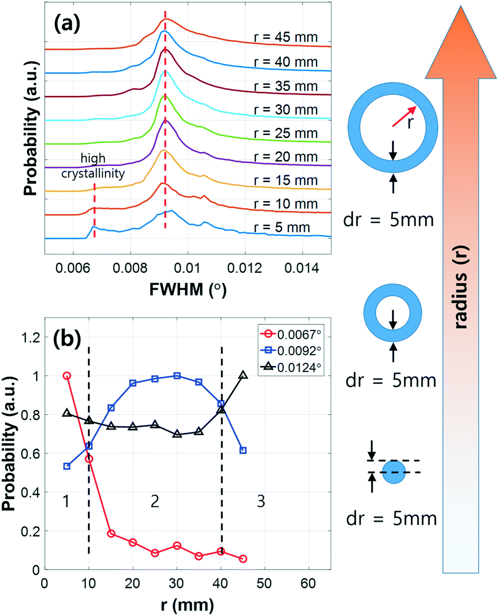 | ||
| Fig. 3 (a) FWHM distribution as a function of the radius from the wafer center. There exists a very high-crystalline region in the wafer center; the overall quality gradually decreases from the center to the edge. (b) Probability of FWHM as a function of the radius. In region 1, the lower angular value of 0.0067° decreases rapidly. In region 2, the FWHM distribution does not change much with the angle. In region 3, the probability of 0.0124° increases rapidly, indicating a relatively low crystallinity. | ||
We evaluated the curvature at different azimuthal angles of ϕ = 0 and 120°. Fig. 4(a) and (b) are obtained from the peak positions at the respective detector pixels. If we trace a line profile across the wafer center [Fig. 4(c) and (d)], we observe a constant radius of curvature in the wafer center in both directions at ϕ = 0 and 120°, respectively. However, the values at the wafer edge are lower than those at the wafer center implying an azimuthal angle dependence of the bending of the wafer. According to Seo et al.,23 they showed homogeneous radii of curvature of 20.4 and 20.8 m at ϕ = 0 and 120°, which are smaller than our results (∼35 m), evaluated from the center of Fig. 4(a) and (c), but uniform due to the isotropic wafer bending. To understand the exact lattice-plane tilting, we evaluated the q-vector components to estimate the curvature with respect to the lattice-plane normal direction. Through an operation of two rocking-curve images obtained at two different azimuthal angles and combining them with the rotation matrix R(ux,uy,uz,α), we were able to obtain (qx,qy,qz) vector components of the GaN (114) lattice plane.17 The 3-dimensional rotation matrix R is given explicitly as.22
 | (1) |
 | ||
| Fig. 4 Rocking curve images at ϕ = 0 (a) and 120° (b) are presented along with their corresponding line profiles (c) and (d), respectively. The lattice bending of the wafer edge is higher than that of the wafer center region. | ||
Here, (ux,uy,uz) is the rotation axis with a unit vector and α(x,y,ϕ) is the angle deviation evaluated from the rocking-curve image corresponding to θB(x,y,ϕ) − θave(ϕ), where (x,y,ϕ) denotes the detector positions x and y and the sample azimuthal angle, respectively. To extract the q-vector components, we multiplied the two rotation matrices for ϕ = 0 and 120° with the q-vector of GaN (114) for which the length equals 6.258 Å−1 (= 2π/d114).
 | (2) |
As the qz components are relatively large, we plotted the summation of the qx and qy components [Fig. 5(a)]. The evaluated quiver arrows are directed towards the center of the wafer because of lattice-plane bowing during wafer manufacturing. To visualize this lattice bowing, we calculated the amplitude of the |qx + qy| vectors [Fig. 5(b)]. The center has low amplitude and, with increasing radius, the amplitude tends to increase. From these results, we can estimate that the 4-inch GaN wafer has an anisotropic curvature even though the surface normal direction is flat. To represent the q-vector distribution more simply, we evaluated the distribution of the angles between the q-vectors and surface normal vector [Fig. 5(c)]. The smaller values are from the wafer center; the large values are from the wafer edge and have a mean tilting angle of 0.03°, which is similar to that of a previous report.17 The radius of curvature evaluated from this value is about 50 m, which was larger than that in a previous report on a 2-inch GaN homo-epitaxy.23
 | ||
| Fig. 5 (a) The evaluated (qx,qy) vector components of the 4-inch GaN; the arrows are directed towards the wafer center implying that the lattice planes have a concave shape. The blue points outside the wafer come from parasitic scattering or detector noise. (b) Amplitude of the q-vectors. (c) Angular distributions evaluated from the inner product of qx + qy with qz of the wafer; the lower tilting angles are from the wafer center and the higher values originate from the wafer edge. | ||
3 Conclusion
We have observed the crystallinity of a 4-inch GaN wafer substrate. The image reconstructed from the maximum intensity indicated an inhomogeneous intensity distribution. The evaluated FWHM images indicated a higher crystal quality for the seed crystal than for the grain boundaries grown from seed crystals. The crystallinity of the wafer tended to decrease from its center to its edge. The q-vector analysis of GaN (114) at two different azimuthal angles revealed the overall curvature for which the qx and qy vector components were directed towards the wafer center. We believe our proposed technique will be useful in understanding the crystal quality deviations of large size wafers.
Conflicts of interest
There are no conflicts of interest to declare.Acknowledgements
The measurements were performed at the beamline BL20B2 at SPring-8 under Proposal No. 2017B1029. This work was supported by the Ministry of Education, Culture, Sports, Science and Technology (MEXT) through the “Program for research and development of next-generation semiconductor to realize energy-saving society.”References
- S. Nakamura, T. Mukai, M. Senoh and N. Iwasa, Jpn. J. Appl. Phys., 1992, 31, L139–L142 CrossRef CAS.
- H. Amano, M. Kito, K. Hiramatsu and I. Akasaki, Jpn. J. Appl. Phys., 1989, 28, L2112–L2114 CrossRef CAS.
- Y. Wu, D. Kapolnek, J. P. Ibbetson, P. Parikh, B. P. Keller and U. K. Mishra, IEEE Trans. Electron Devices, 2001, 48, 586–590 CrossRef CAS.
- W. Saito, Y. Takada, M. Kuraguchi, K. Tsuda, I. Omura, T. Ogura and H. Ohashi, IEEE Trans. Electron Devices, 2003, 50, 2528–2531 CrossRef CAS.
- A. Segmüller, J. Angilelo and S. J. La Placa, J. Appl. Phys., 1980, 51, 6224 CrossRef.
- R. Dwiliński, R. Doradziński, J. Garczyński, L. P. Sierzputowski, A. Puchalski, Y. Kanbara, K. Yagi, H. Minakuchi and H. Hayashi, J. Cryst. Growth, 2008, 310, 3911–3916 CrossRef.
- Y. Cui, X. Hu, X. Xie, R. Wang and X. Xu, CrystEngComm, 2017, 19, 3844–3849 RSC.
- D. Gan, Y. Song, W. Sun, L. Guo and X. Chen, J. Phys. D: Appl. Phys., 2015, 48, 435105 CrossRef.
- A. Jafari, I. Sergueev, D. Bessas, B. Klobes, B. S. Roschin, V. E. Asadchikov, P. Alexeev, J. Härtwig, A. I. Chumakov, H.-C. Wille and R. P. Hermann, J. Appl. Phys., 2017, 121, 044901 CrossRef.
- X. Xu, R. P. Vaudo, C. Loria, A. Salant, G. R. Brandes and J. Chaudhuri, J. Cryst. Growth, 2002, 246, 223–229 CrossRef CAS.
- B. Raghothamachar, G. Dhanaraj, J. Bai and M. Dudley, Microsc. Res. Tech., 2006, 69, 343–358 CrossRef CAS PubMed.
- K. Barla, G. Bomchil, R. Herino, J. C. Pfister and J. Baruchel, J. Cryst. Growth, 1984, 68, 721–726 CrossRef CAS.
- Y. Lou, C. Song, Y. Chen, L. S. R. Kumara, N. Palina, O. Seo, S. Hiroi, K. Kajiwara, M. Hoshino, K. Uesugi, Y. Irokawa, T. Nabatame, Y. Koide and O. Sakata, CrystEngComm, 2018, 20, 2861–2867 RSC.
- D. Lübbert, C. Ferrari, P. Mikulík, P. Pernot, L. Helfen, N. Verdi, D. Korytár and T. Baumbach, J. Appl. Crystallogr., 2005, 38, 91–96 CrossRef.
- P. Mikulík, D. Lübbert, P. Pernot, L. Helfen and T. Baumbach, Appl. Surf. Sci., 2006, 253, 188–193 CrossRef.
- A. T. Macrander, S. Krasnicki, Y. Zhong, J. Maj and Y. S. Chu, Appl. Phys. Lett., 2005, 87, 194113 CrossRef.
- J. Kim, O. Seo, C. Song, S. Hiroi, Y. Chen, Y. Irokawa, T. Nabatame, Y. Koide and O. Sakata, Appl. Phys. Express, 2018, 11, 081002 CrossRef.
- C. Chen, C. Zhu, E. R. White, C. Chiu, M. C. Scott, B. C. Regan, L. D. Marks, Y. Huang and J. Miao, Nature, 2013, 496, 74–77 CrossRef CAS PubMed.
- T. Tanikawa, K. Ohnishi, M. Kanoh, T. Mukai and T. Matsuoka, Appl. Phys. Express, 2018, 11, 031004 CrossRef.
- K. Kobayashi, A. A. Yamaguchi, S. Kimura, H. Sunakawa, A. Kimura and A. Usui, Jpn. J. Appl. Phys., 1999, 38, L611–L613 CrossRef CAS.
- K. Motoki, T. Okahisa, S. Nakahata, N. Matsumoto, H. Kimura, H. Kasai, K. Takemoto, K. Uematsu, M. Ueno, Y. Kumagai, A. Koukitu and H. Seki, J. Cryst. Growth, 2002, 237–239, 912–921 CrossRef CAS.
- D. J. Huggins, J. Comput. Chem., 2014, 35, 377–385 CrossRef CAS PubMed.
- O. Seo, J. M. Kim, C. Song, Y. Lou, L. S. R. Kumara, S. Hiroi, Y. Chen, Y. Katsuya, Y. Irokawa, T. Nabatame, Y. Koide and O. Sakata, AIP Adv., 2018, 8, 075318 CrossRef.
Footnote |
| † Present affiliation: NISSAN ARC, LTD., 1 Natsushima-cho, Yokosuka, Kanagawa, 237-0061 Japan. |
| This journal is © The Royal Society of Chemistry 2018 |