DOI:
10.1039/C8CE00229K
(Paper)
CrystEngComm, 2018,
20, 2861-2867
Synchrotron X-ray diffraction characterization of the inheritance of GaN homoepitaxial thin films grown on selective growth substrates†
Received
11th February 2018
, Accepted 23rd April 2018
First published on 3rd May 2018
Abstract
The crystallinity of one n-GaN (Si-doped) and two p-GaN (Mg-doped) homoepitaxial thin films selectively grown on GaN substrates was evaluated by using synchrotron X-ray diffraction. A reflection-mode monochromatic X-ray topography image from the n-GaN homoepitaxial thin film shows a mesh-shape structure that is similar to that of the selective-growth GaN substrate. Moreover, transmission-mode white-beam X-ray topography images from the GaN substrate and the n-GaN homoepitaxial thin film show similar regular dot-shape diffraction patterns. This suggests that, following hydride vapor phase epitaxy, the structural characteristics of the selectively grown GaN substrates inherited from their corresponding foreign substrates (dot-patterned sapphire) were inherited by the subsequent n-GaN homoepitaxial thin film, although the crystal quality of the homoepitaxial thin film had been deteriorated. White-beam topography images from two p-GaN homoepitaxial thin films grown on the same GaN substrate wafer and cut from adjacent areas indicate that the p-GaN thin films were non-uniform.
1 Introduction
GaN, a wide direct bandgap semiconductor, is an important material for fabrication of shortwave light-emitting diodes and laser diodes as well as power electronic devices.1–6 If a high-quality GaN crystal is adopted, the thickness would be 1/10 that of a Si MOS transistor because of its high dielectric breakdown electric field (10 times that of Si), the 2D electron density being as high as 1013 cm−2.7 As a result, low power losses and high voltages and currents are expected if GaN is used as a vertical power semiconductor. However, because there are some difficulties in the growth of single crystals of bulk GaN, researchers have had to grow GaN films on other foreign substrates, such as sapphire, gallium arsenide, silicon, and silicon carbide.8 There are well-known significant differences in the lattice parameters and coefficients of thermal expansion between GaN and other substrates that could inevitably lead to lattice strains and defects (e.g., grain boundaries and threading dislocations) in the film, decreasing the device performance. For several decades, many research institutions and laboratories have devoted many resources to improve the wafer size and crystal quality of the bulk GaN9–23 and homoepitaxial layers.24–32 Currently, hydride vapor phase epitaxy (HVPE) is a promising method to produce GaN substrates in batch quantities, with large size and high crystal quality. Substrates prepared with this growth method have become commercially available in recent years. However, in regard to the current status of the technology, high-quality crystals that match the theoretical characteristics of GaN semiconductors have not been attained. A selective growth method would provide advantages, including a substrate with a lower dislocation density and less substrate warpage. One of the concerns of the growth method is the in-plane non-uniformity of the substrate which has been poorly characterized or observed. For HVPE, the growth method employs a mask placed over the foreign substrate.33–37 In this method, a buried stripe or dot-pattern structure made of metal or oxide was inscribed on the foreign substrate (usually sapphire or GaAs). A series of crack-free mirror-like surfaces is expected to develop on a large-size GaN substrate in consequence of the pinning effect of the mask. However, to date, the results remain unclear.
Efficient techniques of evaluation38–40 are also important in establishing growth methods for industrial purposes and useful for understanding physical properties. In this report, the crystallinity and in-plane non-uniformity of GaN homoepitaxial thin films from the same company were evaluated using synchrotron X-ray diffraction as well as monochromatic X-ray topography, white-beam topography and rocking-curve measurements. The effects of the mask were clearly observed and verified.
2 Experimental aspects
2.1 Samples
Five samples supplied by the same company were used for the experiments. The first sample (designated W) was an as-polished free-standing GaN 2 inch wafer. The second sample (designated S) was an as-polished free-standing GaN 10 mm × 10 mm substrate, and the other three samples (designated N, P1, and P2) were homoepitaxial GaN samples on free-standing GaN substrates grown by metal–organic chemical vapor deposition (MOCVD). All GaN substrates were grown by hydride vapor phase epitaxy (HVPE) under atmospheric pressure with metallic gallium (Ga), hydrochloric acid (HCl) and ammonia (NH3) as sources. The starting substrates were grown using the selective growth method, which employed dot-pattern MOCVD GaN films on Al2O3 substrates as the foreign substrate. The GaN crystals were co-doped with silicon and oxygen; the carrier concentration was around 2 × 1018 cm−3. The grown bulk GaN crystal was sliced into several wafers with small miscut angles (0.4°) towards the [![[1 with combining macron]](https://www.rsc.org/images/entities/char_0031_0304.gif) 100] direction. After slicing, both the front and back surfaces of the wafers were polished. The wafers were 2 inch diameter disks with a thickness of 280 μm. The GaN substrates used in our experiments were obtained from different GaN bulk crystals. We chose the 2 inch wafer W as one of our experimental target samples. The sample S was cut from the GaN freestanding substrate into a 10 mm × 10 mm square shape. The n-GaN homoepitaxial thin film sample N has a 5 μm-thick silicon doping layer with a concentration of 2 × 1016 cm−3 directly grown on the substrate via MOCVD. The shape of this sample was a one quarter piece of the 2 inch diameter disk. The p-GaN homoepitaxial thin film samples P1 and P2 comprised a 2 μm thick undoped layer and a 2 μm thick magnesium-doped layer with a concentration of 3.5 × 1019 cm−3. They were cut from adjacent areas of the same epitaxial wafer. P1 and P2 were 10 mm × 8 mm square shaped. The information on the samples is listed in Table 1.
100] direction. After slicing, both the front and back surfaces of the wafers were polished. The wafers were 2 inch diameter disks with a thickness of 280 μm. The GaN substrates used in our experiments were obtained from different GaN bulk crystals. We chose the 2 inch wafer W as one of our experimental target samples. The sample S was cut from the GaN freestanding substrate into a 10 mm × 10 mm square shape. The n-GaN homoepitaxial thin film sample N has a 5 μm-thick silicon doping layer with a concentration of 2 × 1016 cm−3 directly grown on the substrate via MOCVD. The shape of this sample was a one quarter piece of the 2 inch diameter disk. The p-GaN homoepitaxial thin film samples P1 and P2 comprised a 2 μm thick undoped layer and a 2 μm thick magnesium-doped layer with a concentration of 3.5 × 1019 cm−3. They were cut from adjacent areas of the same epitaxial wafer. P1 and P2 were 10 mm × 8 mm square shaped. The information on the samples is listed in Table 1.
Table 1 Sample information. All substrates were double-face polished free-standing GaN crystals
| Sample name |
Film |
Doping concentration |
Film thickness |
|
W
|
None |
1.6 × 1018 cm−3 |
0 μm |
|
S
|
None |
1.4 × 1018 cm−3 |
0 μm |
|
N
|
Si-Doped layer |
2.0 × 1016 cm−3 |
5 μm |
|
P1 |
Mg-Doped layer |
3.5 × 1019 cm−3 |
2 μm |
|
P2 |
Mg-Doped layer |
3.5 × 1019 cm−3 |
2 μm |
2.2 Monochromatic X-ray topography
X-ray topography is a method enabling a visualization of the strain field of the lattice caused by defects (e.g., threading dislocations, basal plane dislocations, stacking faults and grain boundaries) in a crystal. Such information allows the quality of the crystal to be assessed and facilitates the means to reduce defects during crystal growth. Monochromatic X-ray topography employs an incident beam with parallel and monochromatic X-rays. The wavelength of the incident X-ray was 1.284 Å, and the diffraction vector used was g = 11![[2 with combining macron]](https://www.rsc.org/images/entities/char_0032_0304.gif) 4 (θB = 39.73°, incident angle θ0 = 0.589° if the sample has no miscut angle). The whole sample surface was irradiated by the incident beam. Two 2D X-ray detectors were alternately used. The detector used for the 2 inch wafer was a flat panel sensor (C7942, Hamamatsu Photonics) with a pixel size of 50 μm per pixel and an active area of 112 × 118 mm2 (2240 × 2368 pixels), by which the whole sample can be observed at once. The exposure time used was 440 ms. For the other samples, we used an X-ray imaging detector comprising a beam monitor AA60 and an ORCA Flash 4.0 sCMOS camera (Hamamatsu Photonics) with a pixel size of 8.1 μm per pixel and an area of 16 mm × 16 mm. The exposure time was one second. We rotated the sample around the [100] axis to record the diffraction images for several set angles near the 114 Bragg angle with a fixed sample position and detector angle and position (see Fig. S1 in the ESI†). These measurements were performed at the beamline BL20B2, SPring-8.
4 (θB = 39.73°, incident angle θ0 = 0.589° if the sample has no miscut angle). The whole sample surface was irradiated by the incident beam. Two 2D X-ray detectors were alternately used. The detector used for the 2 inch wafer was a flat panel sensor (C7942, Hamamatsu Photonics) with a pixel size of 50 μm per pixel and an active area of 112 × 118 mm2 (2240 × 2368 pixels), by which the whole sample can be observed at once. The exposure time used was 440 ms. For the other samples, we used an X-ray imaging detector comprising a beam monitor AA60 and an ORCA Flash 4.0 sCMOS camera (Hamamatsu Photonics) with a pixel size of 8.1 μm per pixel and an area of 16 mm × 16 mm. The exposure time was one second. We rotated the sample around the [100] axis to record the diffraction images for several set angles near the 114 Bragg angle with a fixed sample position and detector angle and position (see Fig. S1 in the ESI†). These measurements were performed at the beamline BL20B2, SPring-8.
2.3 Rocking curve
The incident X-ray wavelength was 1.55 Å with a beam size of 0.1 mm × 0.1 mm. We recorded the variation of the diffraction intensities with the incident angle, i.e., the rocking curve, near the 0002 Bragg angle θB using a Si-pin detector fixed around 2θB = 34.82°. We evaluated and compared the crystal perfection of different sample positions according to the peak height and width of the absolute reflectivity normalized by the incident beam intensity. The positions were inferred from the monochromatic X-ray topography images. The X-ray extinction distance for the 0002 Bragg peak was 4300 Å, evaluated using the dynamical theory of X-ray diffraction. The measurements were performed at the NIMS beamline BL15XU, SPring-8.
2.4 White-beam X-ray topography
Distinct from monochromatic X-ray topography, white-beam topography uses the full X-ray bandwidth of the incoming beam (a non-monochromatic beam), without any wavelength filtering. In this experiment, a white incident X-ray beam was used for a transmission geometry, and the diffraction intensity was recorded by an ORCA detector. Two incident-beam sizes were used. One was a 2 mm × 2 mm beam to obtain diffraction topography images. The other was 10 mm wide by 0.01 mm high for data collection, which involved repeated measurements taken at different sample heights. The latter allows us to efficiently record diffraction curves for several sample positions. The samples were tilted from the vertical to the incident beam side by 3° so that the 110 diffraction appears for an incident X-ray wavelength of 0.1670 Å. The schematic diagram of the white-beam X-ray topography experimental setup is shown in Fig. S2 in the ESI.† This experiment was performed at the beamline BL28B2, SPring-8.
3 Results and discussion
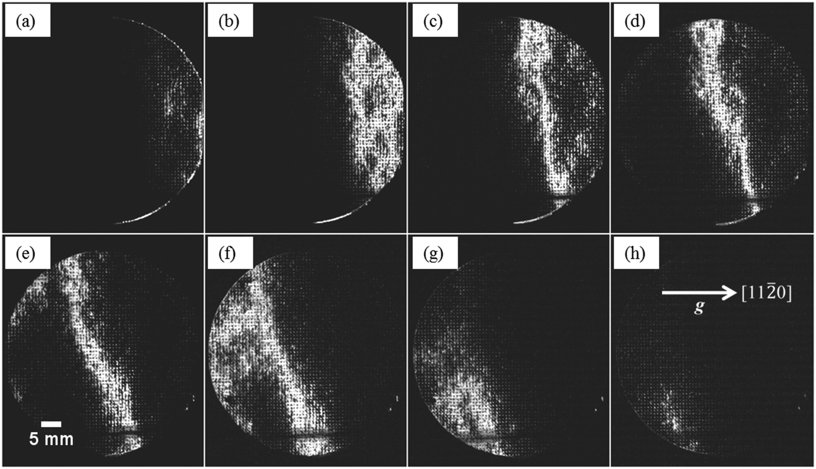
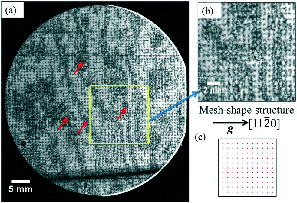
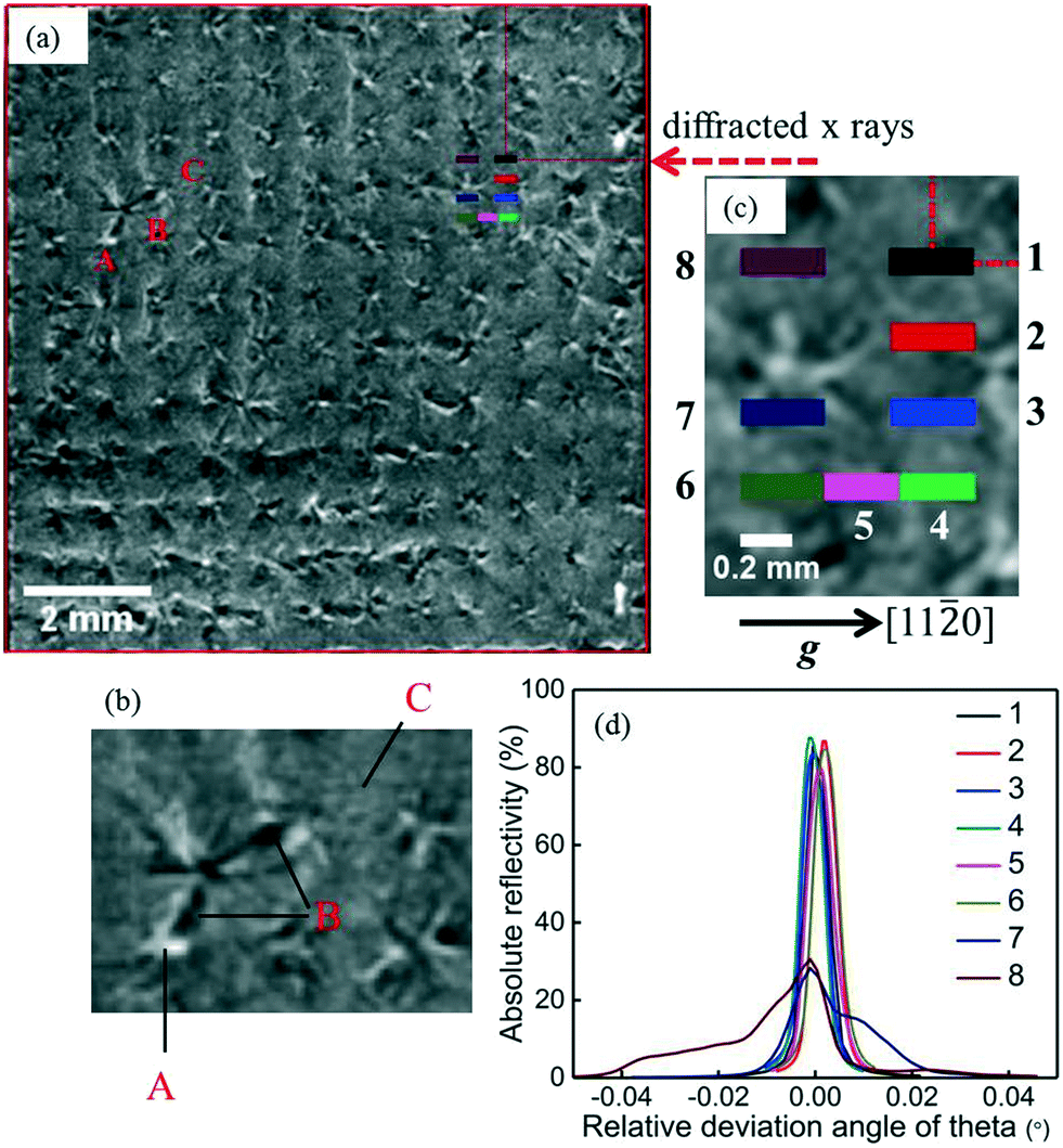
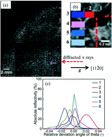
We observed the macroscopic shape of sample W using the results of monochromatic X-ray topography. The diffraction images (Fig. 1) were recorded at increments of 50 arcsec with the flat panel detector. White patches designate stronger diffraction intensities than black patches. Bragg diffraction takes place in small areas at a fixed incident angle, and the white patches move with increasing incident angle, indicating that the normal to the (114) plane is changed along [100]. We superimposed all the monochromatic X-ray topography images recorded at different incident angles. This allows us to characterize the domain orientations and crystalline quality. Fig. 2(a) shows a superimposed image obtained from all images in Fig. 1. A series of black curved bands in the superimposed pattern of sample W [indicated by red arrows in Fig. 2(a)] may come from our measurements (more exactly, come from the overlapped measurement regions between the two adjacent incident angles). Furthermore, the enlarged view in Fig. 2(b) shows a mesh-shape structure, which originated from the selective growth GaN substrate by the dot-pattern layer on the sapphire substrate [Fig. 2(c)]. The white patches correspond to sample areas of high crystal quality whereas black patches are sample regions with low crystal quality. A superimposed monochromatic X-ray topographic image of S [Fig. 3(a)] recorded with the ORCA detector shows a mesh-shape structure. We estimated the average size of the mesh-shape domains to be approximately 0.85 mm × 0.85 mm, which basically originate from the dot-pattern mask used on the sapphire substrate. The pinning regions of high dislocation density should be either white (marked as “A”) or black (marked as “B”) patches [as shown in the magnified image in Fig. 3(b)]. The drastic variation of diffraction intensity indicated non-uniform crystallinity implying the edge of an integrated crystal grain, which means that this area corresponds to a grain-boundary region created by the dot-pattern.33–37 The gray area (marked as “C”) should have uniform diffraction intensity which originates from an integrated crystal grain with high crystal quality. To characterize the crystal quality quantitatively, we recorded the rocking curves associated with the 0002 reflection for several different positions to compare with the results from the monochromatic X-ray topography images. We chose eight locations around a region of drastic variation of diffraction intensity [see Fig. 3(c)], to measure their 0002 rocking curves [Fig. 3(d)]. The rocking curves of the points (positions 1–6), which are far from the regions of drastic variation of diffraction intensity, have narrow widths and high absolute reflectivities (around 80%), whereas those in the boundary region (positions 7 and 8) have wide widths and low absolute reflectivities (about 20%) (see details in Table S1 in the ESI†).
 |
| | Fig. 1 Diffraction patterns of sample W recorded with the flat panel detector. Each image shows a 114 diffraction pattern at different incident angles with increments of 50 arcsec. The incident angle increases from (a) to (h). | |
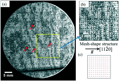 |
| | Fig. 2 (a) The pattern for sample W is a superimposition using all the images in Fig. 1. The red arrows show a series of black curved bands that may come from our measurements (more exactly, come from the overlapped measurement regions between the two adjacent incident angles). Enlarged view (b) of the rectangular area in (a). The mesh-shape structure originates from a selective growth GaN substrate with a dot-pattern layer. The white patches correspond to sample areas of high crystal quality, whereas the black patches correspond to sample regions with more dislocations. Schematic of the dot-pattern layer on the sapphire substrate (c). | |
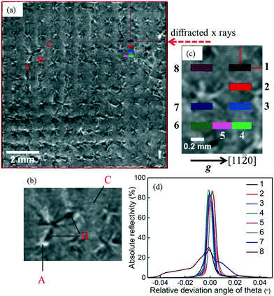 |
| | Fig. 3 Monochromatic X-ray topographic image of sample S recorded with the ORCA detector (a). Image of the mesh-shape structure (resulting from the dot-pattern layer on the sapphire substrate) of the GaN substrate grown by the selective growth method. Magnified image around A, B, and C (b). A white (marked as “A”) or black spot (marked as “B”) is an area of greater dislocations, whereas the gray area (marked as “C”) corresponds to a region of high crystal quality. The color filled rectangles in (c) show positions for 0002 rocking curves (d) normalized by the incident X-ray intensity. | |
Fig. 4(a) shows a monochromatic X-ray topography image of N recorded with the ORCA detector. This sample also has a mesh-shape structure. We recorded the rocking curves for selected areas from the homoepitaxial layers [Fig. 4(c); the detailed information is listed in Table S2 in the ESI†]. Comparing Fig. 4(c) and 3(d), all the rocking curves from N are broader and the absolute reflectivities lower (around 40%). In addition, the relative angles of deviation of the Bragg positions for N are located in a broader angular range. This implies that the epitaxial layer has low crystalline quality with less homogeneity.
 |
| | Fig. 4 Monochromatic X-ray topographic image of sample N recorded with the ORCA detector (a). Color filled rectangles in (b) show positions corresponding to 0002 rocking curves (c) normalized by the incident X-ray intensity. | |
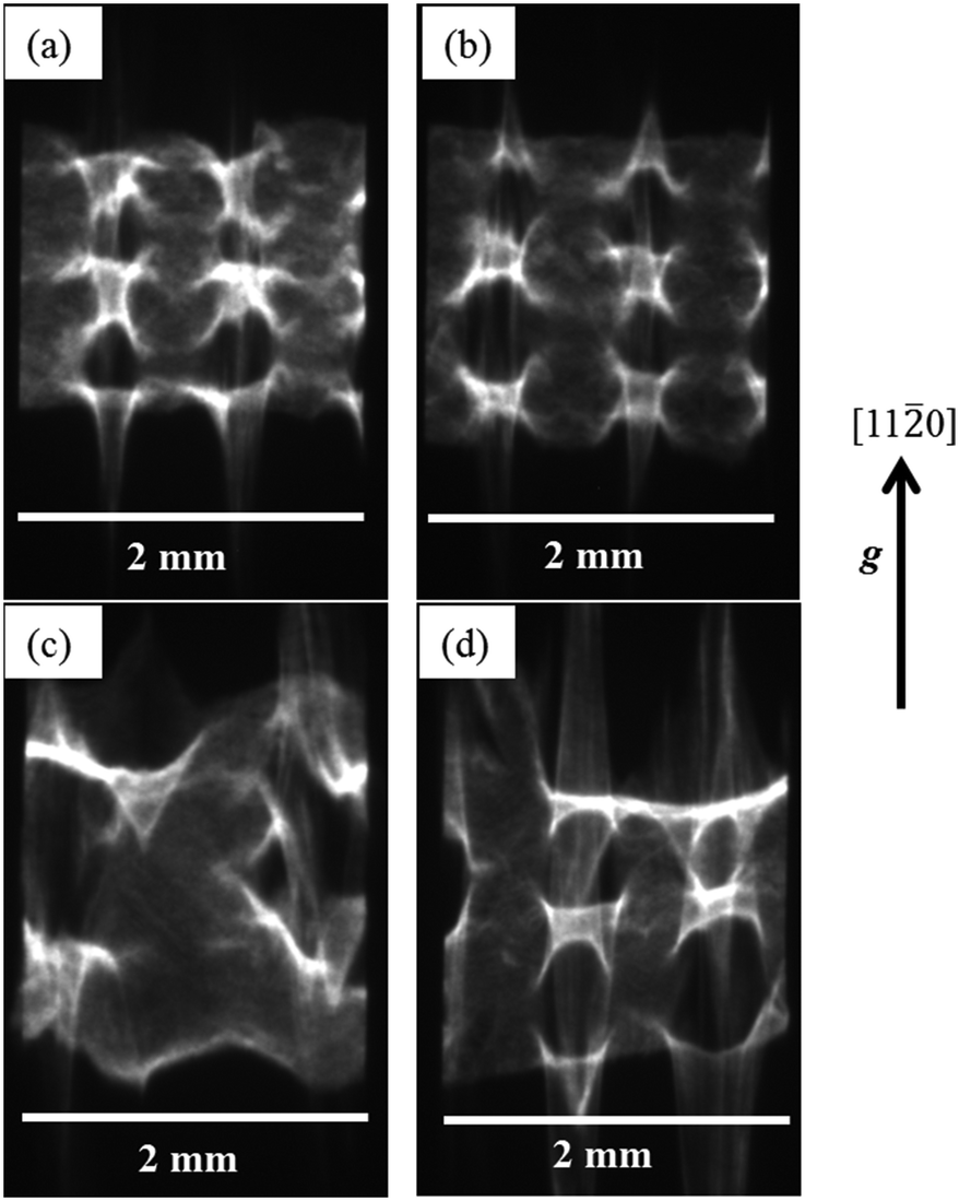
To obtain information on crystal perfection within a larger area, we performed white-beam X-ray topography in transmission mode. Fig. 5 shows various 110 diffraction images for a beam size of 2 mm × 2 mm. The whole area should have a uniform intensity under Bragg conditions if the sample crystallinity is perfect enough. A diffraction image should show a perfectly regular dot-shape pattern when a dot-pattern structure is inherited from the foreign substrate. Fig. 5(a) and (b) for S and N, respectively, show a regular periodicity that originates from the periodicity of dislocation concentrated points (dot-patterns). The images of samples S [Fig. 5(a)] and N [Fig. 5(b)] look consistent with the results of monochromatic X-ray topography [Fig. 3(a) and 4(a)]. We, however, hardly see such a periodicity in Fig. 5(c) for P1, which shows a slightly distorted periodicity, indicating the bad inheritance of the p-GaN homoepitaxial thin film from its substrate. In order to confirm this conclusion, we measured another sample P2, which was cut from an adjacent area of the same wafer as sample P1 using the same method [see Fig. 5(d) for P2], and further verified the bad heredity of p-GaN. The different images in Fig. 5(c) and (d) indicate a significant inhomogeneity in the wafer. Furthermore, the white patches in all four images result from sample regions corresponding to high crystal quality areas with less dislocations, whereas the black patches with weaker intensity arise from lower crystal quality areas with more dislocations, whereas there are medium dislocation densities in the gray areas.37
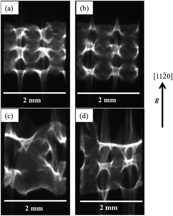 |
| | Fig. 5 White-beam X-ray 110-diffraction topography images in transmission mode. λ = 0.1670 Å, θB = 3°. Sample S (a), sample N (b), sample P1 (c), and sample P2 (d). (c) and (d) are from samples cut from adjacent areas of the same wafer. The white areas with stronger intensity in all four images derive from sample regions corresponding to high crystal quality areas with less dislocations; the black patches with weaker intensity derive from lower crystal quality areas with more dislocations, while there are medium dislocation densities in the gray areas.37 The incident beam size used was 2 × 2 mm2. | |
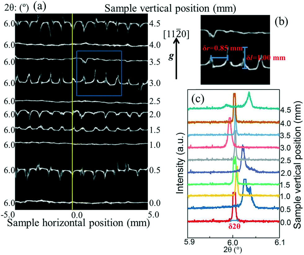
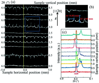
To investigate the position dependence of the d-spacing and angular distribution of the net planes, we recorded white-beam topography images for various horizontal positions of the sample at fixed vertical positions (see Fig. S2 in the ESI†) and a beam size of 0.01 mm (height) × 10 mm (lateral). In addition, we repeated X-ray exposure after changing the vertical position. Fig. 6(a) shows images superposed for different vertical positions obtained from sample N. The intensity profiles in Fig. 6(a) show local variations of the 2θ values as a function of the horizontal position of the sample. That is, the height difference δl in Fig. 6(b) [magnified view of the square area in Fig. 6(a)] on the intensity profile shows differences in the 2θ angle and indicates the differences among the diffraction surface orientations, which can be expressed as δθ = arctan(δl/L), where δθ is the distribution of the net-plane orientation, δ2θ is the width of each peak in Fig. 6(c), and L is the camera length between the sample and the detector used (L = 523 mm). For example, when δl = 1 mm, δθ = 0.11°, which shows the distribution of the (110) net-planes. The diffraction images from N [Fig. 6(a)] look periodic in the horizontal axis direction of the sample. The average periodicity along the lateral direction Δr is approximately 0.85 mm [Fig. 6(b)]. Fig. 6(c) shows an example of the diffraction intensity profiles at the same lateral position for each sample [the vertical line position in Fig. 6(a)]. The Bragg angles vary widely among the different vertical positions, and originate mainly from the angular distribution of the net planes and partly from the difference in the d-spacing and in their positions.
 |
| | Fig. 6 Images of diffraction (a) obtained from sample N [sample in Fig. 5(b) for various heights]. Enlarged view (b) of the rectangle area in (a). Diffraction intensity profile (c) at the vertical line position in (a). The incident beam size used was 10 × 0.01 mm2. | |
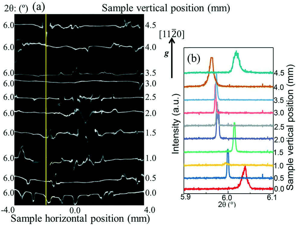
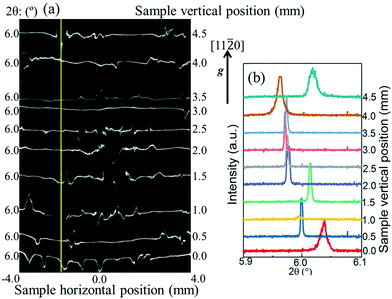
Fig. 7 shows the images recorded from sample P2. Fig. 7(a) lacks any regularity compared with Fig. 6(a). Fig. 7(b) shows examples of diffraction intensity profiles at the same lateral positions [the vertical line position in Fig. 7(a)] as those in Fig. 6(c). The Bragg angle distributions for sample P2 exhibit a strong dependence on the vertical line positions we chose in Fig. 7(a). Fig. S3 and S4 (see the ESI†) show diffraction images from all the samples for comparison. The images from S and N exhibit similar regularities, indicating that the main features of S were inherited by N. However, the group for sample P (namely, P1 and P2) looks to have less regularity and an inhomogeneous structure.
 |
| | Fig. 7 Diffraction images (a) as a function of height from sample P2 (sample in Fig. 5(d)). Diffraction intensity profile (b) at the vertical line position in (a). The incident beam size used was 10 × 0.01 mm2. | |
The results of monochromatic X-ray topography show similar mesh-shape structures in the images of N and S, indicating that the structural information was inherited from the substrate to the n-GaN (Si-doped) homoepitaxial thin film, although the crystal quality and domain orientation uniformity of the epitaxial layer were deteriorated in terms of the results of the rocking curves. Furthermore, the images of white-beam X-ray topography in the transmission mode for S and N show a regular periodicity that originates from the periodicity of dot-patterns that may be from dislocation concentrated points. It is consistent with the results of monochromatic X-ray topography. However, we can hardly see such periodicity in the images of P1 and P2 [two adjacent p-GaN (Mg-doped) homoepitaxial layers in a same wafer], which indicates that the p-type GaN homoepitaxial layer has a poor inheritance from its substrate. All the results above lead to a consistent conclusion that the structural characteristics of the selective growth GaN substrate were inherited from the Al2O3 substrate, and then transferred to the homoepitaxial thin film, although the n-type GaN homoepitaxial layer had a better inheritance than the p-type ones.
4 Conclusion
The crystal quality of large-size n-GaN and p-GaN homoepitaxial layers grown on selective growth GaN substrates (supplied by the same company) has been characterized using synchrotron monochromatic X-ray topography, white-beam X-ray topography, and X-ray-rocking curve measurements. All of the monochromatic X-ray topography images recorded from a GaN 2 inch wafer, a 10 mm × 10 mm substrate, and an n-GaN homoepitaxial thin film on a GaN substrate show mesh-shape domains. The white and black patches in Fig. 3(a) and 4(a) should have high dislocation concentrations, corresponding to contributions from the dot-pattern mask area on the foreign substrate, whereas the gray regions have low dislocation areas and high crystallinity, which is desirable in GaN devices. From the absolute reflectivities of the 0002 rocking curves, we conclude that both the crystal quality and domain orientation uniformity deteriorated after epitaxial growth. Similar to the results of monochromatic X-ray topography, the white-beam X-ray topography images in transmission mode for the GaN substrate and n-GaN homoepitaxial thin film on the GaN substrate show similar regularity and dot-shape diffraction patterns, and the sample was penetrated from front to end, confirming that the dot-pattern structure was inherited from the dot-pattern mask of the foreign substrate (sapphire) to the GaN substrate and then to the n-GaN homoepitaxial film. The white regions in Fig. 5(a) and (b) should have higher crystallinity areas with low dislocation concentrations, which are desirable for GaN devices. The nearby black regions have lower crystallinity with a high number of defects. These results are consistent with the results of monochromatic X-ray topography. Samples P1 and P2 were cut from adjacent areas on the same wafer. We then expected to obtain similar images from them. Fig. 5(c) from sample P1, however, looks quite different from Fig. 5(d) from sample P2. We observed a more regular dot-shape diffraction pattern in Fig. 5(d). Compared with the homoepitaxial thin films for n-GaN, the homoepitaxial thin films for p-GaN may have worse homogeneity and weaker in-plane periodicity. The experiment results reported provide an important reference value for the company supplying the samples and can facilitate the development of the GaN growth process, contributing to an improvement in the quality of GaN single crystals and thin films.
Conflicts of interest
There are no conflicts of interest to declare.
Acknowledgements
The measurements were performed at the NIMS Synchrotron X-ray Station (beamline BL15XU) at SPring-8 under Proposal No. 2016B4502 and 2017A4504 and at the SPring-8 for general beamlines under Proposals No. 2016B1027, 2016B1028, 2016B1031, 2017A1030, 2017A1033, and 2017B1029. This work was supported by the Ministry of Education, Culture, Sports, Science and Technology (MEXT) through the “Program for research and development of next-generation semiconductor to realize energy-saving society”. We thank Richard Haase, PhD, from Edanz Group (http://www.edanzediting.com/ac), for editing a draft of this manuscript.
References
- H. P. Maruska and J. J. Tietjen, Appl. Phys. Lett., 1969, 15, 327–329 CrossRef CAS.
- M. A. Khan, A. Bhattarai, J. N. Kuznia and D. T. Olson, Appl. Phys. Lett., 1993, 63, 1214–1215 CrossRef CAS.
- S. Nakamura, T. Mukai, M. Senoh and N. Iwasa, Jpn. J. Appl. Phys., 1992, 31, L139–L142 CrossRef CAS.
- H. Amano, M. Kito, K. Hiramatsu and I. Akasaki, Jpn. J. Appl. Phys., 1989, 28, L2112–L2114 CrossRef CAS.
- S. Nakamura, Science, 1998, 281, 956–961 CrossRef CAS.
- S. Nakamura, Phys. World, 1998, 11, 31–35 CrossRef CAS.
-
S. Taranovich, EDN network, 2013, March 15 Search PubMed.
- G. Wang and X. L. Chen, Phys. Status Solidi A, 2010, 207, 2757–2768 CrossRef CAS.
- S. T. Kim, Y. J. Lee, D. C. Moon, C. H. Hong and T. K. Yoo, J. Cryst. Growth, 1998, 194, 37–42 CrossRef CAS.
- X. Xu, R. P. Vaudo, C. Loria, A. Salant, G. R. Brandes and J. Chaudhuri, J. Cryst. Growth, 2002, 246, 223–229 CrossRef CAS.
- Y. Oshima, T. Eri, M. Shibata, H. Sunakawa, K. Kobayashi, T. Ichihashi and A. Usui, Jpn. J. Appl. Phys., 2003, 42, L1–L3 CrossRef CAS.
- K. Fujito, S. Kubo, H. Nagaoka, T. Mochizuki, H. Namita and S. Nagao, J. Cryst. Growth, 2009, 311, 3011–3014 CrossRef CAS.
- X. B. Li, J. J. Wu, N. L. Liu, T. Han, X. N. Kang, T. J. Yu and G. Y. Zhang, Mater. Lett., 2014, 132, 94–97 CrossRef CAS.
- H. Gu, G. Q. Ren, T. F. Zhou, F. F. Tian, Y. Xu, Y. M. Zhang, M. Y. Wang, Z. Q. Zhang, D. M. Cai, J. F. Wang and K. Xu, J. Alloys Compd., 2016, 674, 218–222 CrossRef CAS.
- B. Wang, M. J. Callahan, K. D. Rakes, L. O. Bouthillette, S.-Q. Wang, D. F. Bliss and J. W. Kolis, J. Cryst. Growth, 2006, 287, 376–380 CrossRef CAS.
- R. Dwiliński, R. Doradziński, J. Garczyński, L. P. Sierzputowski, A. Puchalski and Y. Kanbara,
et al.
, J. Cryst. Growth, 2009, 311, 3015–3018 CrossRef.
- R. Dwilińsk, R. Doradziński, J. Garczyński, L. P. Sierzputowski and R. Kucharski,
et al.
, J. Cryst. Growth, 2010, 312, 2499–2502 CrossRef.
- H. Yamane, M. Shimada, S. J. Clarke and F. J. DiSalvo, Chem. Mater., 1997, 9, 413–416 CrossRef CAS.
- W. J. Wang, X. L. Chen, Y. T. Song, W. X. Yuan, Y. G. Cao and X. Wu, J. Cryst. Growth, 2004, 264, 13–16 CrossRef CAS.
- X. L. Chen, Sci. Technol. Adv. Mater., 2005, 6, 766–771 CrossRef CAS.
- F. Kawamura, M. Morishita, M. Tanpo, M. Imade, M. Yoshimura, Y. Kitaoka, Y. Mori and T. Sasaki, J. Cryst. Growth, 2008, 310, 3946–3949 CrossRef CAS.
- H. Q. Bao, B. Song, H. Li, G. Wang, W. J. Wang, W. Y. Wang and X. L. Chen, Cryst. Growth Des., 2009, 9, 611–615 CAS.
- I. Grzegory, Mater. Sci. Eng., B, 2001, 82, 30–34 CrossRef.
- H. Amano, N. Sawaki, L. Akasaki and Y. Toyoda, Appl. Phys. Lett., 1986, 48, 353–355 CrossRef CAS.
- T. Detchprohm, K. Hiramatsu, H. Amano and I. Akasaki, Appl. Phys. Lett., 1992, 61, 2688–2690 CrossRef CAS.
- H. J. Lee, S. Y. Bae, K. Lekhal, T. Mitsunari, A. Tamura, Y. Honda and H. Amano, J. Cryst. Growth, 2016, 454, 114–120 CrossRef CAS.
- S. Porowski, J. Cryst. Growth, 1998, 189/190, 153–158 CrossRef CAS.
- C. R. Miskys, M. K. Kelly, O. Ambacher, G. Martınez-Criado and M. Stutzmann, Appl. Phys. Lett., 2000, 77, 1858–1860 CrossRef CAS.
- C. Kirchner, V. Schwegler, F. Eberhard, M. Kamp, K. J. Ebeling, K. Kornitzer, T. Ebner, K. Thonke, R. Sauer, P. Prystawko, M. Leszczynski, I. Grzegory and S. Porowski, Appl. Phys. Lett., 1999, 75, 1098–1100 CrossRef CAS.
- R. Dwilinski, R. Doradzinski, J. Garczynski, L. P. Sierzputowski, M. Zajac and M. Rudzinski, J. Cryst. Growth, 2009, 311, 3058–3062 CrossRef CAS.
- A. M. Roskowski, E. A. Preble, S. Einfeldt, P. M. Miraglia, J. Schuck, R. Grober and R. F. Davis, Opto-Electron. Rev., 2002, 10, 261–270 CAS.
- M. Leszczyński, H. Teisseyre, T. Suski, I. Grzegory, M. Boćkowski, J. Jun and A. Barski, Acta Phys. Pol., A, 1996, 90, 887–890 CrossRef.
- H. Marchand, X. H. Wu, J. P. Ibbetson, P. T. Fini, P. Kozodoy, S. Keller, J. S. Speck, S. P. DenBaars and U. K. Mishra, Appl. Phys. Lett., 1998, 73, 747–749 CrossRef CAS.
- H. Sone, S. Nambu, Y. Kawaguchi, M. Yamaguchi, H. Miyake, K. Hiramatsu, Y. Iyechika, T. Maeda and N. Sawaki, Jpn. J. Appl. Phys., 1999, 38(4A), L356–L359 CAS.
- Y. Honda, Y. Iyechika, T. Maeda, H. Miyake, K. Hiramatsu, H. Sone and N. Sawaki, Jpn. J. Appl. Phys., 1999, 38, L1299–L1302 CAS.
- M. Haino, M. Yamaguchi, H. Miyake, A. Motogaito, K. Hiramatsu, Y. Kawaguchi, N. Sawaki, Y. Iyechika and T. Maeda, Jpn. J. Appl. Phys., 2000, 39, L449–L452 CAS.
- K. Motoki, SEI Tech. Rev., 2010, 70, 28–35 Search PubMed.
- S. Sintonen, S. Suihkonen, H. Jussila, A. Danilewsky, R. Stankiewicz, T. O. Tuomi and H. Lipsanen, Appl. Phys. Express, 2014, 7, 091003 CrossRef.
- L. Kirste, A. N. Danilewsky, T. Sochacki, K. Köhler, M. Zajac, R. Kucharski, M. Boćkowski and P. J. McNally, ECS J. Solid State Sci. Technol., 2015, 4, P324–P330 CrossRef CAS.
- N. A. Mahadik, S. B. Qadri and J. A. Freitas Jr, Cryst. Growth Des., 2015, 15, 291–294 CAS.
Footnote |
| † Electronic supplementary information (ESI) available. See DOI: 10.1039/c8ce00229k |
|
| This journal is © The Royal Society of Chemistry 2018 |
Click here to see how this site uses Cookies. View our privacy policy here. 
 Open Access Article
 This Open Access Article is licensed under a Creative Commons Attribution-Non Commercial 3.0 Unported Licence
 b,
Yanna
Chen
bc,
Loku Singgappulige Rosantha
Kumara
b,
Yanna
Chen
bc,
Loku Singgappulige Rosantha
Kumara