
Effect of deposition pressure on the structural and optical properties of Ga2O3 films obtained by thermal post-crystallization
Yikai
Liao
,
Shujie
Jiao
 *,
Shaofang
Li
,
Jinzhong
Wang
,
Dongbo
Wang
,
Shiyong
Gao
,
Qingjiang
Yu
and
Hongtao
Li
*,
Shaofang
Li
,
Jinzhong
Wang
,
Dongbo
Wang
,
Shiyong
Gao
,
Qingjiang
Yu
and
Hongtao
Li
School of Materials Science and Engineering, Harbin Institute of Technology, Harbin, 150001, People's Republic of China. E-mail: shujiejiao@hit.edu.cn
First published on 24th November 2017
Abstract
β-Ga2O3 films have been obtained by thermal annealing of amorphous thin films that were deposited by radio frequency magnetron sputtering. The influence of deposition pressure on the properties of the β-Ga2O3 films was investigated. The structural and optical properties of the β-Ga2O3 films were evaluated using X-ray diffraction, X-ray photoelectron spectroscopy, scanning electron microscopy and optical spectrophotometric measurements. The full width at half maximum of β-Ga2O3 (600) X-ray diffraction peaks decreased firstly and then increased with increasing deposition pressure. A similar variation tendency was observed for the optical band gap of the β-Ga2O3 films. The reasons were attributed to joint action of the atoms' diffusion ability on the surface and oxygen partial pressure with deposition pressure. With increasing pressure, sputtered target species collided more and lacked energy to diffuse leading to poorly crystallized films. With high deposition pressure, oxygen partial pressure also increased in the deposition chamber, thus crystalline quality was improved due to the decrease in oxygen vacancies in the film, which was confirmed by investigating O 1s and Ga 3d core levels using X-ray photoelectron spectroscopy.
Introduction
Wide band gap semiconductors are considered as the foundation of future devices because of their attractive properties and potential applications. Among them, in recent years, gallium oxide (Ga2O3) has been attracting increasing attention in the application to solar-blind ultraviolet (UV) detectors,1 high-power2 and high-voltage electronic devices.3 Besides, Ga2O3 has been studied for application to gas sensors,4 photocatalysis,5 light emitting diodes6 and hydrogen generation7 due to its wide band gap of 4.8–4.9 eV and high breakdown electric field of 8 MV cm−1.Ga2O3 has several different polymorphic structures, including α-Ga2O3, β-Ga2O3, γ-Ga2O3, δ-Ga2O3 and ε-Ga2O3.8 Among these, β-Ga2O3 is regarded as the most stable phase that could be converted from other metastable phases at high temperature.9 Because of its outstanding chemical stability, most device applications of Ga2O3 are based on β-Ga2O3. In recent years, various methods such as radio frequency (RF) magnetron sputtering,10–12 pulse laser deposition,13,14 molecular beam epitaxy,15 and chemical vapor deposition16,17 have been employed to fabricate β-Ga2O3 thin films. Among these methods, RF magnetron sputtering is widely used to deposit Ga2O3 thin films because of its low cost, easy manipulation and high film adhesion.18 Since β-Ga2O3 crystallization could only be realized at relatively high temperature, β-Ga2O3 is obtained at elevated substrate temperature during film deposition in the majority of the literature.19–21 Alternatively, there is another way to realize crystallization of β-Ga2O3 by post-annealing amorphous Ga2O3 films that have been deposited onto an unheated substrate at room temperature (RT) or low temperature, which is called solid-phase crystallization.22 This method has relatively low requirements for equipment and ensures sufficient reliability. In this method, room-temperature deposition leads to amorphous nanocrystalline films, which consist of a great amount of tiny crystalline grains with short-range order and chaotic orientation resulting from random atomic arrangements.23 Thermal post-annealing drives randomly arranged atoms to crystallize along the tiny crystalline grains, which could be considered as the nucleus,24 leading to the macroscopic crystallized films. The post-annealing parameters have been studied roundly and precisely in other studies25–27 including the annealing temperature, type of annealing and annealing gaseous environment. Not only the annealing process but also the properties of as-grown amorphous films have a great influence on the films. However, the properties of as-grown amorphous films and annealed films have been seldom studied under different sputtering conditions using the fixed annealing process.
In this paper, β-Ga2O3 thin films are obtained by a two-step method: thermally annealing the amorphous films deposited by radio frequency magnetron sputtering at RT (substrate temperature). The dependence of the structural and optical properties of as-grown films and annealed β-Ga2O3 films on the deposition pressure was studied in detail.
Experimental
As-grown thin films were deposited on quartz glass substrates by radio frequency magnetron sputtering. Prior to deposition, using a chemical procedure, the quartz glass substrates were cleaned with acetone, ethanol and deionized water for 15 min for each step before sputtering.28 A sintered ceramic Ga2O3 target of 99.99% purity was employed for sputtering. The substrate temperature was fixed at room temperature during sputtering. The sputtering power was set to 150 W. The flow rates of O2 and Ar gases were fixed at 5 sccm and 40 sccm, respectively. In order to study the influence of deposition pressure, the deposition pressure was set from 0.5 to 3 Pa. The deposition duration for each sample was 120 min. After sputtering deposition, the films were thermally annealed at a fixed temperature of 650 °C in a quartz tube furnace in an air atmosphere for 2 h. The temperature was increased at a rate of 10 °C min−1. After heating was stopped, the samples were cooled down until the temperature reached room temperature. A scanning electron microscope (SEM, Hitachi SU70) was employed to investigate the film morphology and measure the film thickness. X-ray diffraction (XRD) patterns were collected with a diffractometer (Rigaku D/max-2600/PC) using Cu Kα radiation (λ = 0.15418 nm) to characterize the crystallographic properties of the films. X-ray photoelectron spectroscopy was used to characterize the element state (PHI 5700 ESCA system). The peaks were calibrated using the adventitious C 1s peak at 284.6 eV. The optical transmittance spectrum of each sample was obtained in the wavelength range of 200–800 nm using a UV-vis spectrophotometer (TU-1901).Results and discussion
Film morphology
To obtain information about the film morphology, the top view of the as-grown films was measured with SEM, given in Fig. 1. Prior to imaging, gold specimens were coated because of the insulating nature of the films. The film deposited at 0.5 Pa consists of micro-crystal grains with irregular grain gaps, as shown in Fig. 1(a). When the deposition pressure was increased to 1.5 Pa, the grain size slightly decreased and the number of voids was greatly reduced. As the pressure increased to 3 Pa, a film with a smooth surface and uniform grain size was deposited. The observed morphology change with increasing deposition pressure is in good accordance with the modified Thornton model for TCOs.29,30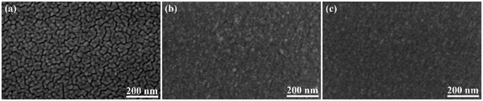 | ||
| Fig. 1 Top view of as-grown Ga2O3 films by SEM at (a) 0.5 Pa, (b) 1.5 Pa and (c) 3 Pa. | ||
Film thickness was also evaluated using SEM cross-sectional images. Typical cross-sectional images of as-grown Ga2O3 films deposited at 0.5 Pa, 1.5 Pa and 3 Pa are shown in Fig. 2(a–c). The variation of film thickness with deposition pressure is summarized in Fig. 2(d). The thicknesses of the films deposited under different deposition pressures are in the range of 300 ± 10 nm. Considering film unevenness introduced by keeping the substrate unrotated during deposition, changing the deposition pressure from 0.5 Pa to 3 Pa did not affect the deposition rate significantly. Considering the sputtering process, more ionized gas particles impacting the target led to more sputtered species with increasing deposition pressure. On the other hand, more sputtered species result in more collision between them and less kinetic energy to diffuse on the surface. Meanwhile, low growth temperature also decreases energy-driven diffusion. Under these two conditions, the thickness of the film only changes slightly.
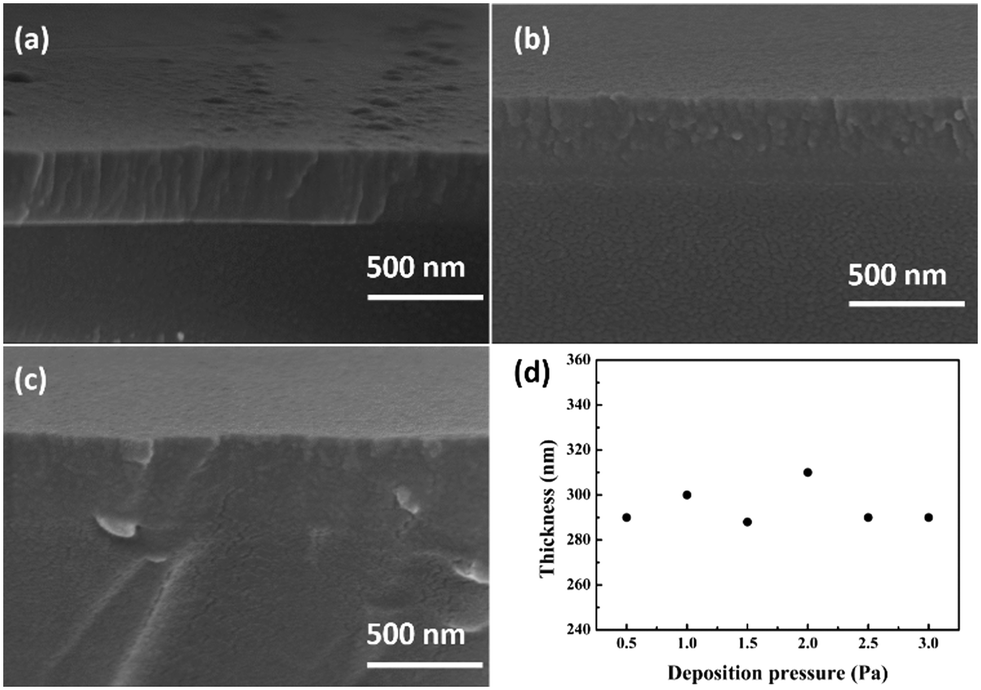 | ||
| Fig. 2 SEM cross-sectional images of as-grown Ga2O3 films deposited at (a) 0.5 Pa, (b) 1.5 Pa and (c) 3 Pa and (d) summarized variation of film thickness with deposition pressure. | ||
A schematic diagram of the deposition process was proposed to represent the morphology evolution of the as-grown films with deposition pressure, as shown in Fig. 3. When the deposition pressure was 0.5 Pa, the amount of grown species was not enough, and the effect of energetic bombardment was significant, thus adatoms tended to fly away from the deposited surface, which perturbs the grain growth, leading to nonuniform grain sizes and defects, as shown in Fig. 3(a). As the deposition pressure increased up to 1.5 Pa, the particle bombardment effect was reduced because of increasing collision among sputtered species, thus leading to the decrease of grain size and the number of defects, as depicted in Fig. 3(b). When the deposition pressure was increased to 3 Pa, the effect of ion bombardment was further reduced and oxygen was increased, thus a smooth surface with uniform and finely packed grains was observed, as shown in Fig. 3(c).
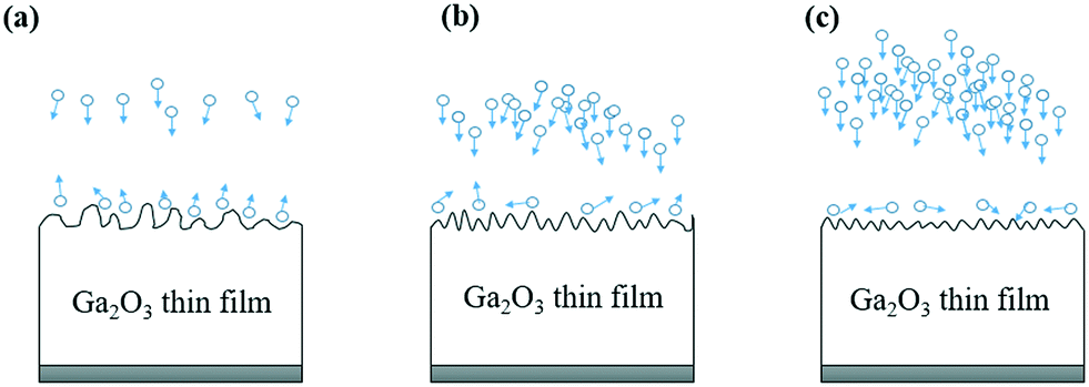 | ||
| Fig. 3 Schematic diagram of as-grown Ga2O3 films deposited at (a) 0.5 Pa, (b) 1.5 Pa and (c) 3 Pa in the sputtering process. | ||
Crystal structure
XRD patterns of as-grown and annealed films are shown in Fig. 4. For the as-grown films, no noticeable peaks can be observed except for the broad profile originating from the quartz glass substrates. This indicated that the as-grown thin films were amorphous (as all as-grown samples showed amorphous characteristics, only one curve was shown in the figure). Low-temperature deposition of amorphous Ga2O3 films was also reported in the literature.31–33 After annealing, broad diffraction peaks at 2θ = 30.2° and 35.6° corresponding to (![[1 with combining macron]](https://www.rsc.org/images/entities/char_0031_0304.gif) 10) and (111) planes and sharp diffraction peaks at 2θ = 44.4°, 64.3° and 64.8° corresponding to (600), (
10) and (111) planes and sharp diffraction peaks at 2θ = 44.4°, 64.3° and 64.8° corresponding to (600), (![[2 with combining macron]](https://www.rsc.org/images/entities/char_0032_0304.gif) 04) and (
04) and (![[7 with combining macron]](https://www.rsc.org/images/entities/char_0037_0304.gif) 12) planes were observed, respectively, indicating that the films changed from their amorphous form to polycrystalline β-Ga2O3 (JCPDS 41-1103). Different XRD patterns suggested that different deposition pressures could influence the properties of the as-grown films, leading to different crystallization via thermal post-annealing. The mechanism of influence has been discussed by analyzing the β(600), β(04) and β(12) planes as follows.
12) planes were observed, respectively, indicating that the films changed from their amorphous form to polycrystalline β-Ga2O3 (JCPDS 41-1103). Different XRD patterns suggested that different deposition pressures could influence the properties of the as-grown films, leading to different crystallization via thermal post-annealing. The mechanism of influence has been discussed by analyzing the β(600), β(04) and β(12) planes as follows.
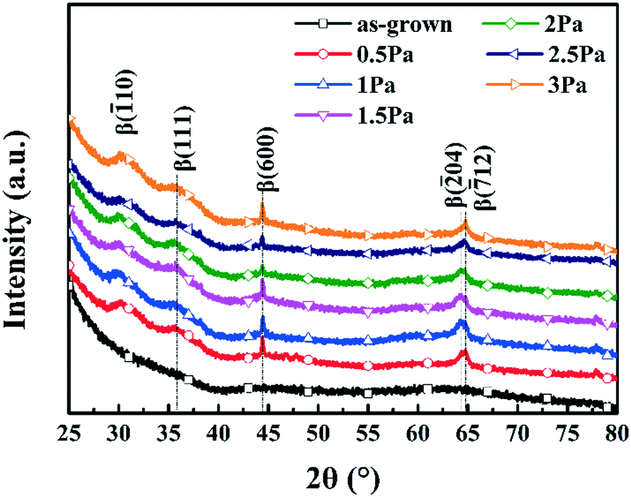 | ||
| Fig. 4 X-ray diffraction patterns of the as-grown films and annealed films deposited under different pressures. | ||
The β-Ga2O3 (600) peak showed the smallest peak width (FWHM) among the diffraction peaks. Fig. 5 shows the lattice structure of monoclinic β-Ga2O3. The (600) plane is considered to be the most stable plane with the largest atomic density and minimum surface free energy in monoclinic β-Ga2O3, thus crystallization along the (600) direction exhibited a fast growth rate compared to the other planes.34,35
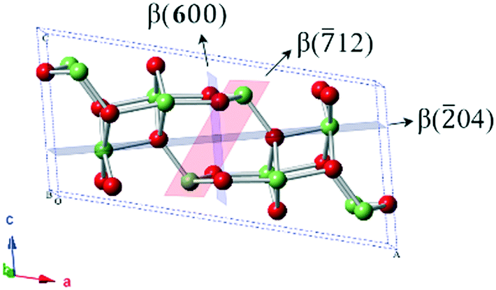 | ||
| Fig. 5 Schematics of the lattice structure of monoclinic β-Ga2O3. | ||
Fig. 6(a) shows the amplified XRD patterns from 43° to 45.5°. Fig. 6(b) shows the influence of deposition pressure on the β(600) peak intensity and full width at half maximum (FWHM). It can be seen that the peak intensities decreased until the deposition pressure reached up to 2 Pa, then increased when the deposition pressure further increased. The FWHM of β(600) diffraction was found to gradually increase when the deposition pressure was varied from 0.5 Pa to 2 Pa but reduced from 2 Pa to 3 Pa. This indicated that only poorer plane texture and smaller grain size could be obtained as the deposition pressure increased to a certain extent, and better plane texture and larger grain size could be achieved again when furthering increasing deposition pressure.
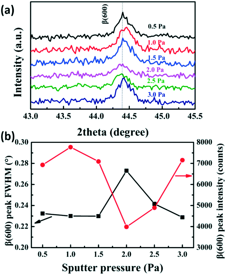 | ||
| Fig. 6 (a) XRD patterns from 43° to 45.5° of Ga2O3 thin films under different deposition pressures; (b) variation of the β(600) peak FWHM and intensity as a function of deposition pressure. | ||
Fig. 7 shows the amplified XRD patterns from 60° to 70°. With increasing deposition pressure, the intensity of the peaks remained high under relatively low deposition pressure from 0.5 Pa to 1 Pa, as shown in Fig. 7(a). Under intermediate deposition pressure from 1 Pa to 2.5 Pa (Fig. 7(b)), both β(04) and β(12) peak intensities gradually decreased. Under high deposition pressure from 2.5 Pa to 3 Pa, the β(04) peak intensity remained constant while the β(12) peak intensity increased (Fig. 7(c)). The plane texture of β(04) and β(12) changed with increasing deposition pressure.
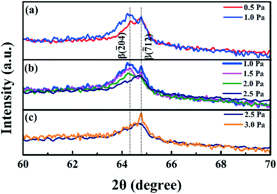 | ||
| Fig. 7 XRD patterns from 2θ = 60° to 70° of annealed films deposited under (a) low deposition pressure, (b) intermediate deposition pressure and (c) high deposition pressure. | ||
In a sputtering system, sputtered target species lacked energy to diffuse due to more collision with increasing the pressure, thus, leading to poorly crystallized films with small grain sizes. Further increasing the deposition pressure also increases the oxygen partial pressure in the deposition chamber, thus oxygen vacancies in the film could reduce, which improves crystallization.34,36 These two factors were supposed to be responsible for the change of XRD diffraction. From 0.5 Pa to 2 Pa, more sputtered species were loaded onto the surface with low energy, inducing small grains and poor crystallization. While from 2 Pa to 3 Pa, enough oxygen in the film increases the crystal quality and diffraction intensity, as shown in Fig. 6 and 7(c). The SEM images in Fig. 1 also confirmed this hypothesis. The film showed discontinuous particles at the surface under low pressure owing to the lack of energy of the sputtered species. With increasing pressure, the surface became smooth with oxygen partial pressure increased. Besides, the β(04) peak intensity kept decreasing from 1 Pa to 3 Pa, indicating that crystallization along this plane was suppressed with increasing deposition pressure. This was because the β(04) plane had the lowest surface atomic density and the other plane having a higher surface atomic density would be easier to form under high pressure.17
Optical properties
Optical transmittance spectra of the as-grown amorphous and annealed films deposited under different deposition pressures are shown in Fig. 8(a) and (b). The high transmittance of over 80% in the visible range suggested that the deposited films have a transparent nature. In addition, obvious Fabry–Perot oscillation could be seen in the visible range suggesting that all films have good interface quality between the film and the substrate.19 A sharp cut-off could be seen in the deep ultraviolet region, suggesting good optical properties of the films. In addition, transmittance edges in the wavelength range of 250 nm to 300 nm for the as-grown and annealed films gradually red-shifted and then blue-shifted with the increase of deposition pressure (insets of Fig. 8(a) and (b)). The tendency was similar to the change of XRD results with increasing the sputtering pressure.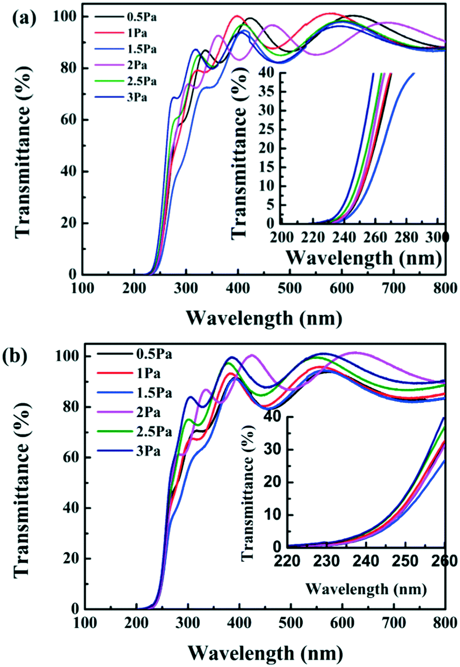 | ||
| Fig. 8 Optical transmittance spectra of (a) as-grown and (b) annealed films. The insets in (a) and (b) show the enlargement of the wavelength region from 200 to 300 nm of the same spectra. | ||
Defects near the band gap edge have an important influence on the semiconductor optical properties. Since the formation energy of oxygen vacancies is much lower than that of gallium vacancies,37 oxygen vacancies are the main defects in the films and their amount has a great influence on the optical properties of β-Ga2O3 films. Higher sputtering pressure resulted in larger oxygen partial pressure, which reduced the amount of defects related to oxygen vacancies, leading to the increase of transmittance and blue-shift.
Further analysis of the optical transmittance spectra was realized to better understand the influence of deposition pressure on optical properties. The optical band gaps of the as-grown and annealed films are determined using a Tauc plot.38 For Ga2O3 with a direct band gap, the absorption obeys the following law:
| (αhν) = B(hν − Eg)1/2 | (1) |
| α = [1/d]In(T) | (2) |
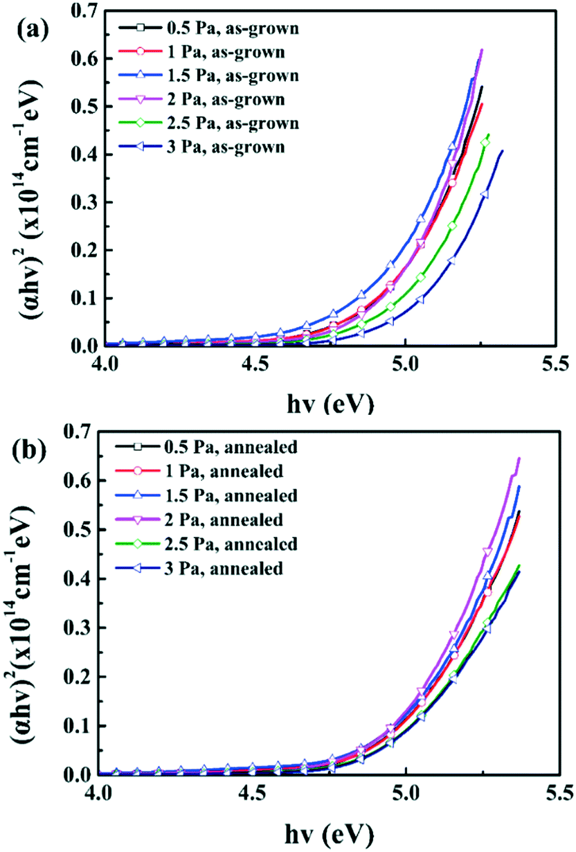 | ||
| Fig. 9 (αhν)2vs. hν plots for (a) as-grown and (b) annealed films. | ||
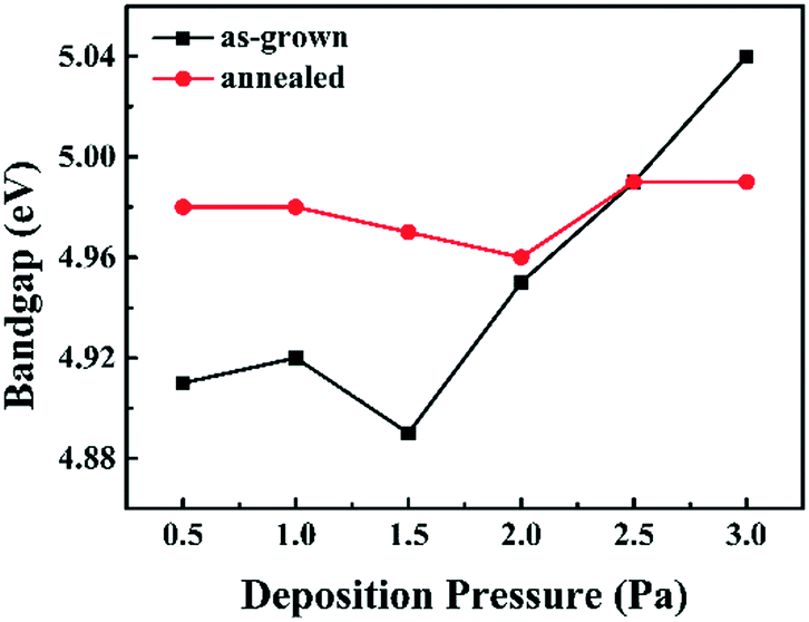
The variation of optical band gaps of the as-grown and annealed films deposited under different deposition pressures is shown in Fig. 10. For the as-grown films, the band gap decreased at low pressure and increased with increasing deposition pressure. For the deposited annealed films, the band gap values also changed similarly to those of the as-grown films under different deposition pressures; however, the data are all in the range from 4.95 eV to 4.99 eV, which is consistent with the reported band gap value of β-Ga2O3 thin films.39,40 Increasing the deposition pressure could enhance the collision between sputtered species from the target, decrease the kinetic energy of arriving particles as well as the grain size of nanocrystals, and increase the band gap value.41 This was observed in other amorphous semiconductor materials like InSb.42 Also, the defect energy level near the band gap greatly influences the band gap values.43 With increasing deposition pressure, the amount of oxygen vacancies was reduced, thus leading to the increase of band gap value. The change of optical band gap with increasing the pressure was in good accordance with the SEM and XRD analyses.
 | ||
| Fig. 10 Variation of band gaps for as-grown and annealed films under different deposition pressures. | ||
Chemical states
The chemical compositions and bonding states of the Ga2O3 thin films were studied by X-ray photoelectron spectroscopy. O 1s and Ga 3d peaks were investigated by comparing as-grown and annealed films under different pressures. Fig. 11(a–d) show the O 1s and Ga 3d core level XPS spectra of the annealed films at 0.5, 1.5 and 3 Pa deposition pressure, respectively. O 1s intensities increased with increasing deposition pressure. The O 1s peak could be deconvoluted into two components: one was at around 530 eV from the contribution of O–Ga bonds of β-Ga2O3 and the other at a higher energy side of around 531–532 eV was from the O2− ions in the oxygen-deficient regions.44,45 The change in oxygen vacancy concentration has been inspected by fitting O 1s peaks under different deposition pressures. Taking the area of peaks into account, O–Ga bond components were enhanced greatly after annealing, which revealed that the concentration of oxygen vacancies decreased due to the annealing and high pressure. The Ga 3d peak with a binding energy of 20.2 eV further confirmed the presence of Ga–O bonds of β-Ga2O3 in the samples, as shown in Fig. 11(d).46 The increase in the peak intensity of Ga–O bonds also illustrated that the oxygen vacancies were suppressed with increasing pressure.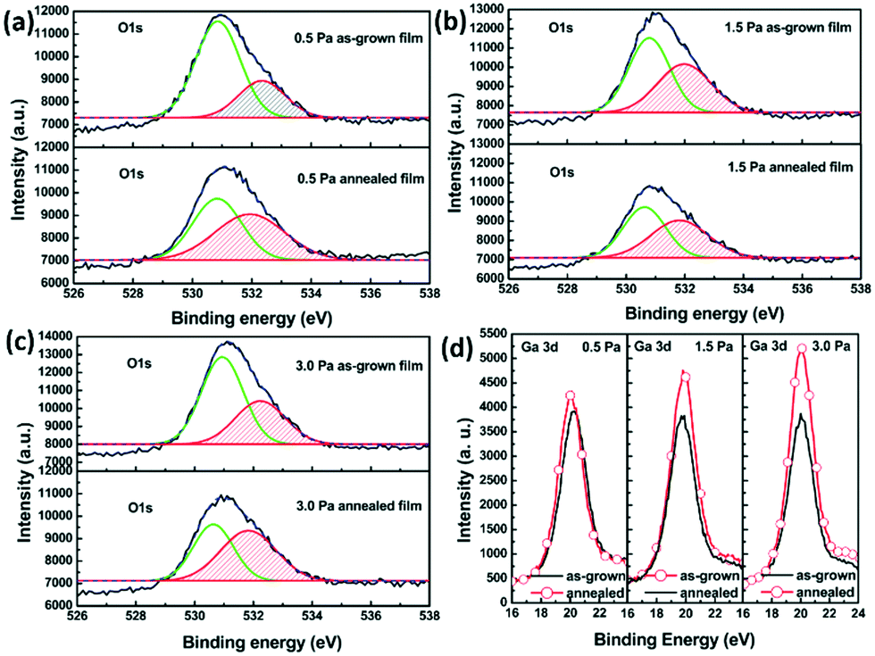 | ||
| Fig. 11 XPS spectra of as-grown and annealed samples, (a) O 1s core level at 0.5 Pa; (b) O 1s core level at 1.5 Pa; (c) O 1s core level at 3.0 Pa; (d) Ga 3d core level. | ||
Conclusions
Amorphous Ga2O3 films have been deposited on quartz glass substrates at room temperature by radio frequency magnetron sputtering under deposition pressures of 0.5, 1, 1.5, 2, 2.5 and 3 Pa. Polycrystalline β-Ga2O3 films were obtained after the annealing process at 650 °C for 2 h. The structural and optical properties of the films were investigated. The optical band gap of β-Ga2O3 with a red and then blue shift was observed as deposition pressure increased. The crystal quality also decreased and then increased as pressure increased. The mechanisms were discussed based on the sputtering process. With increasing pressure, sputtered target species lacked energy to diffuse due to more collision, leading to poorly crystallized films with small grain size. Further increasing the deposition pressure also increased the oxygen partial pressure in the deposition chamber, thus oxygen vacancies in the film could reduce, which improves crystallization. From the XPS measurements, the analysis of the O 1s and Ga 3d core levels confirmed that the oxygen vacancies reduced with pressure and annealing.Conflicts of interest
There are no conflicts to declare.Acknowledgements
This research was supported by the National Natural Science Foundation of China (Grant No. 61306014, 61574051 and 61774051).References
- D. Y. Guo, X. L. Zhao, Y. S. Zhi, W. Cui, Y. Q. Huang, Y. H. An, P. G. Li, Z. P. Wu and W. H. Tang, Mater. Lett., 2016, 164, 364 CrossRef CAS.
- K. Sasaki, A. Kuramata, T. Masui, E. G. Villora, K. Shimamura and S. Yamakoshi, Appl. Phys. Express, 2012, 5, 035502 CrossRef.
- M. Higashiwaki, K. Sasaki, T. Kamimura, M. H. Wong, D. Krishnamurthy, A. Kuramata, T. Masui and S. Yamakoshi, Appl. Phys. Lett., 2013, 103, 123511 CrossRef.
- M. Ogita, K. Higo, Y. Nakanishi and Y. Hatanaka, Appl. Surf. Sci., 2001, 175–176, 721 CrossRef CAS.
- Y. Sakata, T. Nakagawa, Y. Nagamatsu, Y. Matsuda, R. Yasunaga, E. Nakao and H. Imamura, J. Catal., 2014, 310, 45 CrossRef CAS.
- K. H. Kim, S. J. Kim, S. Y. Park and T. G. Kim, J. Nanosci. Nanotechnol., 2015, 15, 7777 CAS.
- S. J. Chang, Y. L. Wu, W. Y. Weng, Y. H. Lin, W. K. Hsieh, J. K. Sheu and C. L. Hsu, J. Electrochem. Soc., 2014, 161, H508 CrossRef CAS.
- R. Roy, V. G. Hill and E. F. Osborn, J. Am. Chem. Soc., 1952, 74, 719 CrossRef CAS.
- S. Ghose, M. S. Rahman, J. S. Rojas-Ramirez, M. Caro, R. Droopad, A. Arias and N. Nedev, J. Vac. Sci. Technol., B, 2016, 34, 02L109 Search PubMed.
- H. C. Kang, Mater. Lett., 2014, 119, 123 CrossRef CAS.
- T. Takeuchi, H. Ishikawa, N. Takeuchi and Y. Horikoshi, Thin Solid Films, 2008, 516, 4593 CrossRef CAS.
- K. Takakura, S. Funasaki, I. Tsunoda, H. Ohyama, D. Takeuchi, T. Nakashima, M. Shibuya, K. Murakami, E. Simoen and C. Claeys, Phys. B, 2012, 407, 2900 CrossRef CAS.
- A. Goyal, B. S. Yadav, O. P. Thakur, A. K. Kapoor and R. Muralidharan, J. Alloys Compd., 2014, 583, 214 CrossRef CAS.
- A. Petitmangin, B. Gallas, C. Hebert, J. Perrière, L. Binet, P. Barboux and X. Portier, Appl. Surf. Sci., 2013, 278, 153 CrossRef CAS.
- X. C. Guo, N. H. Hao, D. Y. Guo, Z. P. Wu, Y. H. An, X. L. Chu, L. H. Li, P. G. Li, M. Lei and W. H. Tang, J. Alloys Compd., 2016, 660, 136 CrossRef CAS.
- W. Mi, J. Ma, C. Luan and H. Xiao, J. Lumin., 2014, 146, 1 CrossRef CAS.
- Y. Chen, H. Liang, X. Xia, R. Shen, Y. Liu, Y. Luo and G. Du, Appl. Surf. Sci., 2015, 325, 258 CrossRef CAS.
- X. Deng, J. Huang, Y. Sun, K. Liu, R. Gao, W. Cai and C. Fu, J. Alloys Compd., 2016, 684, 510 CrossRef CAS.
- X. Z. Liu, P. Guo, T. Sheng, L. X. Qian, W. L. Zhang and Y. R. Li, Opt. Mater., 2016, 51, 203 CrossRef CAS.
- F. B. Zhang, K. Saito, T. Tanaka, M. Nishio and Q. X. Guo, J. Cryst. Growth, 2014, 387, 96 CrossRef CAS.
- S. Rafique, L. Han and H. Zhao, Phys. Status Solidi A, 2016, 213, 1002 CrossRef CAS.
- H. Akazawa, Vacuum, 2016, 123, 8 CrossRef CAS.
- H. Lee and S. Lopatin, J. Appl. Phys., 2003, 93, 3796 CrossRef CAS.
- T. Matuyama, K. Wakisaka, M. Kameda, M. Tanaka, T. Matsuoka, S. Tsuda, S. Nakano, Y. Kishi and Y. Kuwano, Jpn. J. Appl. Phys., 1990, 29, 2327 CrossRef.
- M. Isai, S. Kayano and T. Horiuchi, Trans. Mater. Res. Soc. Jpn., 2010, 35, 897 CrossRef CAS.
- D. Shiojiri, R. Yamauchi, D. Fukuda, N. Tsuchimine, S. Kaneko, A. Matsuda and M. Yoshimoto, J. Cryst. Growth, 2015, 424, 38 CrossRef CAS.
- P. Rao and S. Kumar, Superlattices Microstruct., 2014, 70, 117 CrossRef CAS.
- W. Z. Xie, S. J. Jiao, D. B. Wang, S. Y. Gao, J. Z. Wang, Q. J. Yu and H. T. Li, Appl. Surf. Sci., 2017, 405, 152 CrossRef CAS.
- V. Assunção, E. Fortunato, A. Marques, H. Águas, I. Ferreira, M. E. V. Costa and R. Martins, Thin Solid Films, 2003, 427, 401 CrossRef.
- Z. Zhang, Y. Tang, J. Chen and J. Chen, Phys. B, 2016, 495, 76 CrossRef CAS.
- C. Hebert, A. Petitmangin, J. Perrière, E. Millon, A. Petit, L. Binet and P. Barboux, Mater. Chem. Phys., 2012, 133, 135 CrossRef CAS.
- S. L. Ou, D. S. Wuu, Y. C. Fu, S. P. Liu, R. H. Horng, L. Liu and Z. C. Feng, Mater. Chem. Phys., 2012, 133, 700 CrossRef CAS.
- H. W. Kim and N. H. Kim, J. Alloys Compd., 2005, 389, 177 CrossRef CAS.
- R. Birringer, H. Gleiter, H.-P. Klein and P. Marquardt, Phys. Lett. A, 1984, 10, 365 CrossRef.
- R. Birringer, Mater. Sci. Eng., A, 1989, 117, 33 CrossRef.
- S. Kunj and K. Sreenivas, Curr. Appl. Phys., 2016, 16, 748 CrossRef.
- M. A. Blanco, M. B. Sahariah, H. Jiang, A. Costales and R. Randey, Phys. Rev. B: Condens. Matter Mater. Phys., 2005, 72, 184103 CrossRef.
- S. Sampath Kumar, E. J. Rubio, M. Noor-A-Alam, G. Martinez, S. Manandhar, V. Shutthanandan, S. Thevuthasan and C. V. Ramana, J. Phys. Chem. C, 2013, 117, 4194 Search PubMed.
- D. Shiojiri, D. Fukuda, R. Yamauchi, N. Tsuchimine, K. Koyama, S. Kaneko, A. Matsuda and M. Yoshimoto, Appl. Phys. Express, 2016, 9, 105502 CrossRef.
- G. C. Hu, C. X. Shan, N. Zhang, M. M. Jiang, S. P. Wang and D. Z. Shen, Opt. Express, 2015, 23, 13554 CrossRef CAS PubMed.
- N. Kaur, S. Sharma and D. Kim, Curr. Appl. Phys., 2016, 16, 231 CrossRef.
- T. Dhawan, A. G. Vedeshwar, V. N. Singh, B. R. Mehta and R. P. Tandon, Scr. Mater., 2010, 63, 97 CrossRef CAS.
- M. Al-Kuhaili, S. Durrani and E. Khawaja, Appl. Phys. Lett., 2003, 83, 4533 CrossRef CAS.
- S. L. Ou, D. S. Wuu, Y. C. Fu, S. P. Liu, R. H. Horng, L. Liu and Z. C. Feng, Mater. Chem. Phys., 2012, 133, 700 CrossRef CAS.
- L. Huang, Q. Feng, G. Q. Han, F. G. Li, X. Li, L. W. Fang, X. Y. Xing, J. C. Zhang and Y. Hao, IEEE Photonics J., 2017, 9, 6803708 Search PubMed.
- S. D. Wolter, B. P. Luther, D. L. Waltemyer, R. J. Molnar, C. Onneby and S. E. Mohnry, Appl. Phys. Lett., 1997, 70, 2155 CrossRef.
| This journal is © The Royal Society of Chemistry 2018 |