
 Open Access Article
 This Open Access Article is licensed under a
 Creative Commons Attribution 3.0 Unported Licence
Probing functional self-assembled molecular architectures with solution/solid scanning tunnelling microscopy
Daling
Cui
 a,
Jennifer M.
MacLeod
*b and
Federico
Rosei
*ac
a,
Jennifer M.
MacLeod
*b and
Federico
Rosei
*ac
aINRS-Energy, Materials and Telecommunications and Center for Self-Assembled Chemical Structures, Varennes, Quebec J3X 1S2, Canada. E-mail: rosei@emt.inrs.ca
bSchool of Chemistry, Physics and Mechanical Engineering and Institute for Future Environments, Queensland University of Technology (QUT), Brisbane, 4001 QLD, Australia. E-mail: jennifer.macleod@qut.edu.au
cInstitute for Fundamental and Frontier Science, University of Electronic Science and Technology of China, Chengdu 610054, P. R. China
First published on 6th August 2018
Abstract
Over the past two decades, solution/solid STM has made clear contributions to our fundamental understanding of the thermodynamic and kinetic processes that occur in molecular self-assembly at surfaces. As the field matures, we provide an overview of how solution/solid STM is emerging as a tool to elucidate and guide the use of self-assembled molecular systems in practical applications, focusing on small molecule device engineering, molecular recognition and sensing and electronic modification of 2D materials.
 Daling Cui | Daling Cui received his Bachelor degree in Applied Physics from Tianjin University (2012), China. He holds PhD degree in science of energy and material science from INRS (Canada) and currently continues as a postdoctoral fellow. His research interests mainly focus on the investigation of host–guest structures based on covalent organic frameworks at solution/solid interface. |
 Jennifer M. MacLeod | Jennifer MacLeod is a Senior Lecturer in Physics at the School of Chemistry, Physics and Mechanical Engineering at Queensland University of Technology (QUT). She holds MSc and PhD degrees in Physics from Queen's University (Canada). Jennifer has worked as an NSERC Postdoctoral Fellow at the Università degli Studi di Trieste (Italy) and as Research Associate at INRS (Canada). She currently holds an ARC DECRA Fellowship that is focused on the development of low-energy inverse photoemission spectrometry. Her research interests include self-assembly and reactions of molecules at surfaces, and the growth and modification of graphene and other 2D materials. |
 Federico Rosei | Federico Rosei is Professor and Director of Institut National de la Recherche Scientifique, Énergie, Matériaux et Télécommunications, Université du Québec, Varennes (QC) Canada. Since January 2014 he has held the UNESCO Chair in Materials and Technologies for Energy Conversion, Saving and Storage and since May 2016 he has held the Canada Research Chair (Senior) in Nanostructured Materials. He received MSc and PhD degrees from the University of Rome “La Sapienza” in 1996 and 2001, respectively. Dr Rosei's research interests focus on the properties of nanostructured materials, and on how to control their size, shape, composition, stability and positioning when grown on suitable substrates. His work has been cited over 10 |
Introduction
Scanning tunnelling microscopy (STM) offers an unparalleled view of materials interfaces at the atomic scale.1 Because it operates under a range of conditions, STM can be used to characterize a range of materials: under ultrahigh vacuum, STM can study reactive and/or low-temperature samples, including model systems of e.g. catalysts,2 and novel quantum systems like superconductors3,4 and topological insulators,5 whereas in ambient conditions, STM can investigate the relatively inert surfaces where molecular self-assembly occurs. However, one of the most unique capabilities of STM is its ability for real space visualization of molecular processes at the solution/solid interface. By immersing the STM tip into a droplet of solvent containing molecules of interest, the STM can be used to directly image the self-assembled structures that result from adsorption of the molecules onto the substrate.6–8 This ordered layer is often only one molecule thick; the disordered solvent droplet above precludes the use of most characterization tools to investigate this interface, since spectroscopic and diffractive techniques will tend to probe the overlying solvent droplet rather than the ordered interface layer. For these reasons, STM offers unparalleled insight into the processes associated with molecular self-assembly at the solution/solid interface. We would be remiss not to note that the technique requires attention to detail: the solvent must be carefully selected, as it must wet both the substrate and the tip, it must not contribute to ion current and must volatilize only slowly on the time-scale of the experiments, and the substrate must be inert and atomically ordered even under ambient conditions. Furthermore, all the usual challenges of STM relating to tip preparation, acoustic and electric noise minimization and selection of the feedback parameters must also be surmounted. However, as described below, the insight provided by solution/solid STM more than justifies the time and care required to work within these constraints.At the solution/solid interface, molecular self-assembly is driven by several competing forces. The two primary factors are molecule–molecule interactions and molecule–substrate interactions, which work in concert to define the symmetry and topology of the molecular overlayer structure.9 The molecules studied at the solution/solid interface are often planar, ensuring interaction with the underlying substrate, and are functionalized to promote specific intermolecular interactions that can in turn lead to long-range ordering. Hydrogen bonding interactions10–12 are commonly employed for their directionality and strength; halogen bonding has also recently emerged as a driving force for ordering molecules in 2D layers.13–16 Nondirectional interactions, such as van der Waals (vdW), can also be a useful stabilizing influence, and can be particularly beneficial to ordering when deployed in molecule/substrate couples that adhere to epitaxial constraints. A common example of this can be found in self-assembly driven by alkyl chains, which exhibit a favourable epitaxy on highly ordered pyrolytic graphite (HOPG), and tend to assemble in an interdigitated geometry that maximizes vdW interactions.7,17–19 This combination leads to well-defined, close-packed ordering of alkyls, although the assembly of alkylated molecules with multiple modes of interaction (i.e. moieties with additional functionalization) can be difficult to predict due to the competition between interactions.20 In addition to intermolecular and adsorption interactions, solution/solid self-assembly is also influenced through temperature,21 concentration and solvent effects,22 including solvophobicity or solvent co-adsorption (discussed further below).
This range of contributing factors makes the solution/solid interface a useful testbed for studying the nuances of noncovalent molecular interactions. This complexity also means that our understanding of the thermodynamics governing solution/solid self-assembly is still growing. Of particular concern is the difficulty associated with unravelling the competition between kinetic and thermodynamic factors,23 and in discerning whether an observed structure represents a thermodynamic minimum.24,25 However, in recent years, careful experimentation has led to new insight into this matter. For example, the Gibbs free energy change associated with solution/solid self-assembly has been understood by considering a Born–Haber cycle adapted for the molecule/substrate/solvent system.26,27 Taking a different approach, we used a combination of Monte Carlo modelling of lattice multiplicity with density functional theory (DFT) energetics to show that an observed molecular substitutional solid solution is consistent with a thermodynamic minimum.28 Ongoing work in this area continues to build towards a deeper understanding of the enthalpic and entropic considerations around solution/solid self-assembly, and to move us closer to an increased predictive control over the process.29,30
This accumulating wealth of insights into molecular self-assembly provided by solution/solid STM shows that confinement in two dimensions can be a powerful tool for understanding fundamental molecular interactions, and for exploring the possibilities for engineering nuanced and complex architectures through solution processing. Recent reviews have described a range of demonstrated strengths of solution/solid STM as an experimental probe, including investigations of molecular reactivity31 and patterning,32 elucidation of kinetic and thermodynamic processes,24 and unravelling the details of programmed host/guest assembly in porous molecular networks.33 Here, we focus on an emerging application of solution/solid STM: its utility as an enabling technology for practical applications of solution-processed self-assembled molecular structures.
Compared to UHV STM, solution/solid STM can be deployed quickly, cheaply and easily. This, along with its compatibility with solution processing, positions it as a tool of choice for rapid and routine characterization of molecular systems. In addition to being cheaper and more scalable, solution processing can lead to important differences from vacuum deposition of the same molecules, including pseudopolymorphism34,35 and other solvent-related effects,22e.g., polymorph selection due to the presence of solution flow during the deposition process.36 Solution/solid studies provide a way to observe and understand these effects, and therefore add an important complement to other investigations of dry, applications-ready films. In this Article, we highlight three areas where solution/solid STM shows clear promise at enabling novel applications: small-molecule-based organic electronics, molecular recognition and sensing, and modifications of 2D materials.
Insight into architectures for small-molecule organic electronic devices
At the core of organic electronic devices are active layers made from semiconducting molecular materials. The physics of the device type dictates the electronic characteristics that must be optimized in a given architecture; for example, bulk heterojunctions used in organic photovoltaics must contain p-type and n-type semiconducting molecular films intertwined in close proximity (on the scale of the exciton diffusion distance)37 to facilitate charge separation and transport,38 whereas organic field effect transistors (OFETs) require efficient charge transport through the organic film and control of interface effects (particularly energy level alignment) at the film/electrode points of contact.39 Ambipolar transistors can be sensitive to all of these requirements, since they require easy and balanced transport of both electrons and holes.40 In all cases, nanoscale control of the organic semiconductor stacking structure is key to enabling the desired functional properties.41There are two main approaches to device fabrication from organic semiconductors: they can be based on either polymers or small molecules,42 or sometimes a combination of the two materials types.43,44 Of these systems, STM is best-suited to probing the characteristics of small molecule films,45 with ultrahigh vacuum or ambient STM proving useful for vacuum-deposited organic semiconductor thin films,46–48 and solution/solid STM providing a direct view into the assembly and dynamics that occur in the formation of solution-processed films. In device-relevant films, which are typically of the order of tens to hundreds of nanometres thick, the bottom film interface is buried and can be difficult to characterize, yet solution/solid STM directly visualises the molecular structure at the interface and can be combined with other techniques to understand how the interface structure affects the overall film morphology.
Donor/acceptor networks for bulk heterojunctions
An effective approach to ensuring nanoscale proximity in bulk heterojunctions is to engineer both donor and acceptor compounds into a single covalent dyad, with the caveat that the dyads must pack into films such that they create continuous conduits of each conductor type.49 A number of studies have leveraged solution/solid STM to provide insights into the surface adsorption of these dyads, which, when built from planar, polycyclic aromatics, are well-suited to adsorb on HOPG. Early work based on hexa-peri-hexabenzocoronenes (HBC) covalently linked with either pyrene50 or anthraquinones (AQ)51 used solution/solid STM to investigate the packing of the molecules on HOPG, with a focus on identifying whether phase-segregation of the acceptor and donor components occurred in these dyads. A comparative investigation of donor/acceptor and acceptor/donor/acceptor HBC-based molecules revealed the desired phase segregation in films of the triad.52 A different dyad, based on alkyl-substituted HBC and perylene monoimide (PMI), was shown to pack into a phase-segregated lamellar structure at the solution/HOPG interface, where the lamella comprised planar-adsorbed HBC alternating with tilted π–π stacked PMI.53 In this study, STM imaging was complemented with transistor characterization of a spin-coated thin film on SiO2, which showed well-matched electron and hole mobilities of 3 × 10⁻⁶ cm2 V−1 s−1, whereas ribbon-like crystals whose ordering had been optimized through solvent vapour annealing showed an order of magnitude better mobilities. This result suggests that the spin-coated films on SiO2 may not have possessed the ordering observed on HOPG, or that the order may not have propagated through the film; as we discuss below, HOPG-like interfaces have beneficial effects on supramolecular ordering as compared to SiO2. Recent work on an HBC-based donor/acceptor molecule substituted with six benzothiadiazole (BTZ) units shows that these rigid, planar, highly-symmetric structures, which grow into columnar structures in 3D, pack into well-defined bilayer structures at the trichlorobenzene/HOPG interface.54An alternate approach to creating donor/acceptor arrays is to leverage self-assembly of the two components through programmed recognition, an approach we discuss extensively later in this Review. An early proof-of-principle demonstration of this approach focused on 2D arrays of macrocyclic oligothiophene/C60 fullerene complexes.55 We also explored this approach through the formation of oligothiophene/C60 fullerene host/guest arrays at the solution/HOPG interface, where the porous host lattice was stabilized through hydrogen bonding involving carboxylic acids, and the fullerene guest molecules were weakly adsorbed in the pore. A combination of electrostatic effects and substrate symmetries led to the identical positioning of fullerenes within pores where two or three guest molecules were present, providing a mechanism for forming structurally and stoichiometrically 2D donor/acceptor arrays with nanoscale periodicity.56 A similar approach using star-shaped oligothiophenes at the n-tetradecane/HOPG created a template comprising two different types of cavities, one larger and one smaller.57 Introducing fullerene into the solution resulted in their adsorption in the larger cavity type only, creating an array of fullerenes spaced by empty pores in the oligothiophene network. In both cases, the positioning of donors and acceptors suggested by solution/solid STM imaging is only an indicative first step, since a bulk heterojunction device would require the same structure to propagate upward from the surface through a film. The retention of structure through this 2D to 3D transition is not self-evident, although vacuum microscopy experiments suggest that the presence of C60 molecules within the pores of a supramolecular template can help to facilitate the growth of a second layer of the template in an eclipsed geometry.58
More recently, studies of materials for bulk-heterojunction solar conversion have focused on examining the morphological control of the self-assembly of a single type of molecular charge-carrier. In their studies of an alkoxy substituted benzo[1,2-b:4,5-b0]dithiophene (BDT) building block, Yagai and coworkers used solution/solid STM to elucidate the basic association motifs of the molecule (shown in Fig. 1), which assembles into rosettes stabilized through a hydrogen-bonded core (Fig. 1e).59 X-ray diffraction (XRD) studies show that these rosettes also define the bonding motif for the BDT molecule when it is incorporated into a bulk heterojunction structure with the electron acceptor PC61BM ([6,6]-phenyl-C61-butyric acid methyl ester), where the BDT rosettes stack hierarchically into 1D columnar structures. Heterojunction BDT/PC61BM films showed an improved power conversion efficiency compared to previous experiments involving a similar BDT-based molecule (shown as 1 in Fig. 1f), while maintaining the same bonding motifs. This result suggests that the basic BDT scaffold can be modified for improved functional characteristics without perturbing the desirable molecular association and hierarchical packing.60 Through exploration of a regioisomerically matched set of molecules, the same authors demonstrated the important influence of the hydrogen-bonding interaction driving the self-assembly of these molecular rosettes, in particular showing that an alternative hydrogen-bonded lamellar structure can be accessed by leveraging the positioning of short alkyl side chains.61 Once again, the dominant structural motifs identified by solution/solid STM also appear in device-ready films, demonstrating the efficacy of STM in revealing relevant associations.
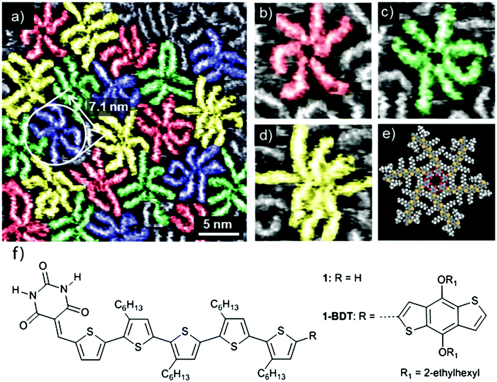 | ||
| Fig. 1 Hydrogen-bonded self-assembly of a benzodithiophene building block at the 1-phenyloctane/HOPG interface. The molecule hydrogen bonds into rosettes that can possess different numbers of molecular constituents (a): six (b), seven (c) or eight (d). A structural model for the six-membered rosette is shown in (e), and for the molecule itself (1-BDT) in (f). STM tunnelling conditions: It = 9 pA, Vs = −0.55 V with a solution concentration of 5.0 × 10⁻⁶ M. Figure adapted from ref. 59 with permission from the Royal Society of Chemistry. | ||
Molecular films for organic field-effect transistors
In small-molecule OFETs, molecular orientation and ordering has a considerable impact on device performance.42 The interface on which the molecular layer is grown can be used to influence the morphology of the resulting film from the bottom up. The effect of the substrate on small-molecule film growth has been extensively studied for the prototypical organic semiconductor pentacene, which grows with its long axis in a near-vertical orientation on inert surfaces, as compared to planar adsorption on metals and semiconductors.62 In molecules functionalized for solubility, the functional groups can dominate the molecule-surface interactions. For example functionalization with triisopropylsilylethynyl (TIPS), which tends to interact strongly with the substrate, renders molecules with pentacene, anthanthrene and dibenzopyrene cores insensitive to the surface free energy of the underlying substrate.63 Other approaches for controlling film morphology can make use of molecular layers: thin templating molecular layers can also be used to control the growth of device-ready films, either from the bottom of the deposited film (molecular template growth)64 or from the top of the film, where an ordered layer (surface segregated monolayer) of low surface-energy molecules can promote ordering through the depth of the film.65Clearly, the presence of a substrate, as is required for STM, creates an opportunity for inducing order in molecular films. Substrate-induced phases (SIP) have been the subject of a comprehensive recent review,66 which details how molecular films may (or may not) change structure at the interface with a solid material. The technical requirements of STM have specific consequences for the SIP observed in typical experiments: the underlying surface is usually ordered and crystalline, meaning that epitaxial molecular overlayers tend to be observed, and STM is best-suited to imaging flat-lying planar molecules, which implies that phases with standing molecules may be avoided because of the intrinsic difficulty in imaging molecules in this configuration. Together, these constraints mean that there may be a selection bias in STM experiments towards systems with rather pronounced SIP characteristics, and which may tend to relax to a different bulk structure once freed from the constraints of planar, epitaxial adsorption.
Graphene, being only a single layer thick, presents an attractive opportunity to introduce orientational control into molecular devices through a SIP and with minimal disruption to the device geometry.67 Near-edge X-ray absorption fine structure (NEXAFS) measurements of chloroaluminium phthalocyanine (ClAlPc) deposited on indium tin oxide (ITO) show that the molecule adsorbs with an average tilt of 45° ± 5° between the molecular plane and the sample surface, whereas ITO coated with monolayer graphene facilitates nearly-planar ClAlPc adsorption (average tilt 10° ± 5°).68 This observation was supported with vacuum STM results that suggested near-planar layer-by-layer growth of the molecule on HOPG, consistent with other work that indicates that graphene and HOPG provide very similar energetic landscapes for molecular self-assembly.21,69 The Goldilocks adsorption regime (not too strong, not too weak) associated with graphene and HOPG provides an adsorption landscape that can facilitate smoother film growth than on either weaker interacting substrates like SiO2, or stronger interacting substrates like metals.70
In our own work, we explored the effects of the substrate, the processing conditions (solution vs. vacuum) and the film thickness on the hydrogen-bond driven self-assembly of N-alkylnaphthalenediimide (NDI-R) semiconductors in 2D and 3D.71 Solution/solid STM reveals that the NDI molecules adsorb in planar geometry on HOPG, with their alkyl chains packed onto the surface at low concentration, or extending away from the surface and into solution at higher concentrations. Following vacuum deposition, this same structure can be observed by STM at the air/HOPG interface although after a two-week aging experiment the film was found to dewet into islands of molecules packed edge-on, the same adsorption geometry that was found for the islands formed within thick films on both HOPG and SiO2. The major difference between these films was found at the interface: whereas planar adsorbed molecules formed the first layer on HOPG, the molecules were edge-on adsorbed directly at the interface for SiO2, suggesting that the system undergoes a Stranski–Krastanov-type growth on HOPG and a Volmer–Weber-type growth72 on SiO2. In this case, although solution/solid STM revealed the predominant intermolecular bonding motif (hydrogen-bonded dimers), the packing geometry enforced by the HOPG surface was not found to propagate into films with device-relevant thicknesses.
However, this knowledge of bonding motifs can be sufficient to elucidate device performance, even if deviations occur between SIP and bulk geometries. We studied the assembly of the brominated π-conjugated molecules 2,5,9,12-tetrabromoanthra[1,2-b:4,3-b′:5,6b′′:8,7b′′′]tetrathiophene and 2,5,9,12-tetrabromoanthra[2,1-b:3,4-b′:6,5-b′′:7,8-b′′′]tetrathiophene (TB2TTA and TB3TTA, respectively) at the 1,2,4-trichlorobenzene (TCB)/HOPG interface and in OTFT devices.73 The DFT-optimized packing geometries for monolayers of the two molecules are shown in Fig. 2a and b and the device characteristics in Fig. 2c and d. The device studies revealed an order of magnitude lower hole mobility in films of TB2TTA as compared to TB3TTA (1.0 × 10⁻⁴ cm2 V−1 s−1 and 2.3 × 10⁻³ cm2 V−1 s−1, respectively). The observed packing at the solution/solid interface indicates that this could be due to the halogen-bond stabilized molecular packing, which suggests multiple S⋯S intermolecular interactions in each TB2TTA unit cell, whereas the TB3TTA cell comprises only a single S⋯S bond; these contacts are thought to contribute to the charge mobility.
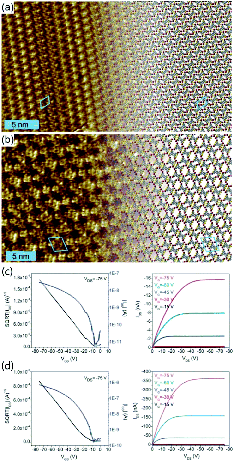 | ||
| Fig. 2 Molecular packing observed at the TCB/HOPG interface for TB2TTA (a) and TB3TTA (b), together with indicative transfer (left) and output (right) characteristics for transistors made from TB2TTA (c) and TB3TTA (d) films. The STM parameters are It = 100 pA and Vt = −800 mV for (a) and It = 300 pA and Vt = −450 mV for (b). This figure is adapted from ref. 73 with permission from the Royal Society of Chemistry. | ||
A different approach to using molecular films for device optimization has been developed by Samorì's group, who recently showed that chemisorbed films of fluorinated mono or biphenylthiols on gold electrodes can improve charge injection in polymer OFETs.74 In their study, the authors solution-deposited their films, then dried them and used STM at the phenyloctane/electrode interface to demonstrate long-range ordering in the molecular layers. In this case, the use of solution/solid STM was incorporated not to directly visualize the solution deposition process, but because the solvent droplet precluded water condensation at the interface and allowed an unfettered observation of the molecular films. This approach to electrode interface engineering produced a number of favourable outcomes, allowing modulation of the surface free energy and the work function at the electrodes, and providing a pathway to tuning these parameters to optimize device performance. It also highlights a novel use of solution/solid STM as a clean, contamination-free approach to imaging molecular films.
Molecular recognition
Nanoscale positioning and recognition of molecules represents an important emerging challenge for future devices.75,76 Molecular recognition, a process involving both binding and selection of substrate by a given molecular receptor as well as possibly a specific function,77 provides a clear framework for implementing this capability. This also builds on an existing body of knowledge: sensing and sorting molecules and has long been an important area in supramolecular chemistry.77–80Two main challenges need to be addressed before implementing this as an approach to sorting in practical applications: (i) how to ensure the occurrence of molecular recognition events; (ii) how to easily measure the presence of the adsorbed molecule. For (i), in conventional solution phase supramolecular chemistry, an event of molecular recognition is typically detected through indirect means, such as changes in the signals of chemical shifts (using nuclear magnetic resonance, NMR) or photophysical properties (using optical spectroscopy like ultraviolet-visible). Such techniques are already highly developed and rigorous.81 They provide a quick, snapshot measurement of ensembles of recognition events. In contrast, STM characterization can provide insightful 2D structural information of individual recognition events in direct space and real time.82 Compared with UHV conditions, the solution/solid interface is an excellent environment for the investigations of molecular recognition because of the tuneable conditions and the dynamic exchange of molecules adsorbed on the surface and in the liquid species which promotes recognition taking place at or close to equilibrium conditions.8 Moreover, the solution phase allows for the facile deposition of several different components simultaneously to examine the selectivity of the molecular receptor.
In practical sensing applications, a measurable signal is required, which is typically obtained through optical, electronic or mechanical transduction of the sensor material. Although the surface-confined recognition process can be straightforward to probe by STM in a controlled experiment, it is difficult to conceive of a rapid or portable sensor based on solution/solid STM to detect the changes in chemical or physical properties associated with molecular recognition. Hence we emphasize that the role of STM is primarily in elucidating the processes and structures associated with molecular recognition at the solution/solid interface.
In the solution/solid geometry, the overlying analyte droplet creates a challenge for direct probing of the surface-confined layer with optical probes. As mentioned previously, solution/solid STM provides a unique view of molecular processes at a submerged interface, with only a few techniques, like neutron scattering, similarly accessing the surface region through the droplet. Hence, evaporation or rinsing of the analyte droplet to allow direct measurement of the interface would likely be required for field-deployed sensing. The insight provided by solution/solid STM can remain relevant after removal of the droplet: structures imaged under solution have been observed after the removal of solvent.83,84 For example, the linear patterns comprising alternating lamellae of 1,3,5-benzene tricarboxylic acid (TMA) dimers and alcohol85 were sustained after drying86 and the host/guest C60/COF-1 structures (see below) were found to be identical at solution/solid and air/solid interfaces.87
Synchronous STM imaging and transduction could be possible using electrochemical STM (EC-STM), which allows simultaneously imaging and performing electrochemical measurements in situ at the solution/solid interface.88 Using EC-STM, the molecular recognition process could be directly observed with microscopy while the corresponding changes in the electrochemical cell can generate an electrical signal, such as current, potential or impedance variations, which can be used as an electrochemical sensor.89 Although EC-STM could potentially combine in situ imaging with transduced sensor signals, STM work to date has focused on investigating molecular recognition with a traditional solution/solid STM, as reviewed in this section.
Selective binding of molecules in a host–guest structure
Building on concepts that have already been well-established in solution,90 molecular recognition at the solution/solid interface can be realized through mutually specific recognition between the surface-confined nanoporous host network and guest molecules, in what is essentially an application of host–guest (H/G) chemistry.81,91 Strategies for introducing selectivity for guest bonding into H/G structures have been predicated on tuning the host geometry, such as pore size,92,93 shape,94 chirality95 or the interactions between host and guest.96 Note that, in addition to selectivity, the reversibility of sensors is another important design parameter. Reversibility requires that the detected molecules can be removed from the sensor through a follow-up treatment, such as annealing, to realize the recycling of sensor. The excessive enhancement of selectivity, i.e., strengthening the interactions between host and guest, may give rise to the difficulty in reversibility. Therefore, a balance must be sought between selectivity and reversibility in real applications for sensors.De Feyter's group has systematically explored approaches to highly selective networks based on the template formed by dehydrobenzo[12]annulenes (DBAs) and its derivatives. DBAs bear six flexible chains, and able to form a porous 2D hexagonal lattice by interdigitating chains to maximize vdW interactions. The alkyl chains can be tuned by the number of methylene groups to scale the size of cavities, and equipped with appropriate functional groups to modify the chemical environment of pores. This allows a range of controls over selectivity. The selectivity imbued by the combination of pore size and shape is demonstrated by the control over the number of triangular nanographene (TNG) guest molecules accommodated in each pore, which shows a clear dependence on the size of cavities.97 Decorating the end of three alternating alkyl chains with azobenzene in which the distal phenyl ring is a dicarboxyazobenzene unit allows two different size pores to be formed by DBA-AZ, allowing adsorption of coronene and hexakis(phenylethynyl)benzene respectively.98 The DBA nanowells, functionalized by fluoroalkane groups, can favourably bind a fluorinated guest over the corresponding hydrocarbon with the same backbone due to the fluoropholicity.96
In addition to pores that adsorb only a single kind of guest molecule, clusters formed by two components can also be immobilized in the nanoscale wells formed by host template. For example, the cluster consisting of one coronene surrounded by six isophthalic acid can be embedded in the hexagonal DBA network via vdW interactions, leading to a three-component 2D crystal.99 Later, a similar system was successful extended to drive formation of a four-component 2D crystal,94,100 These demonstrations of multiple components co-adsorbed in self-assembled structure demonstrate the strict complementarity in size and shape for 2D host–guest complex formation, as well as the controlling influence of functionalization.
Traditionally, the 2D nanoporous host templates have been generated through a number of non-covalent interactions, i.e. hydrogen bonding,56,101,102 van der Waals,103 and metal–ligand interactions.104,105 The reversibility of such supramolecular interactions can foster self-repair in the host template and can in principle lead to defect-free assemblies through the achievement of thermodynamic equilibrium; achieving high crystallinity in the host lattice would be a major boon to investigations and applications of molecular recognition. However, many practical applications or related processing steps require higher stability of the networks, which ultimately demands the strong intermolecular bonds. As an alternative to supramolecular interactions, covalently bonded cavities synthesized in situ on the solid surface acting as hosts can be employed, such as 2D polymers and covalent organic frameworks (COFs).106 COFs define a new class of porous crystalline materials, and have therefore been studied extensively since their first synthesis.107 Their properties include customizable topologies and backbone functionalization, rendering them suitable for a number of applications such as gas separation, energy storage, catalysis, and molecular recognition.107 A high-quality extended hexagonal single layer COF-1108 can be obtained by the self-condensation of 1,4-benzenediboronic acid (BDBA) monomers on highly ordered pyrolytic graphite (HOPG) from heptanoic acid solution in the presence of water, as shown in Fig. 3a and d.109,110 The monolayer COF-1 mesh grows in a 6 × 6 epitaxial unit cell on HOPG with a lattice parameter of 1.476 nm.87 We have demonstrated that such monolayers of COF-1 can act as a host structure to accommodate C60 guest molecules (Fig. 3b). The COF-1 network adsorbs fullerene molecules in two distinct sites: a pore site (P), where the C60 molecule is adsorbed on the underlying HOPG within the pores of BDBA mesh (Fig. 3e and f), and a top site (T), where the fullerene is adsorbed on the boroxine ring of COF-1 (Fig. 3g and h). The stability of these architectures was confirmed through studies of dried COF-1/fullerene films produced by both a drop deposition method and by dipping the HOPG-supported COF-1 into a fullerene solution.
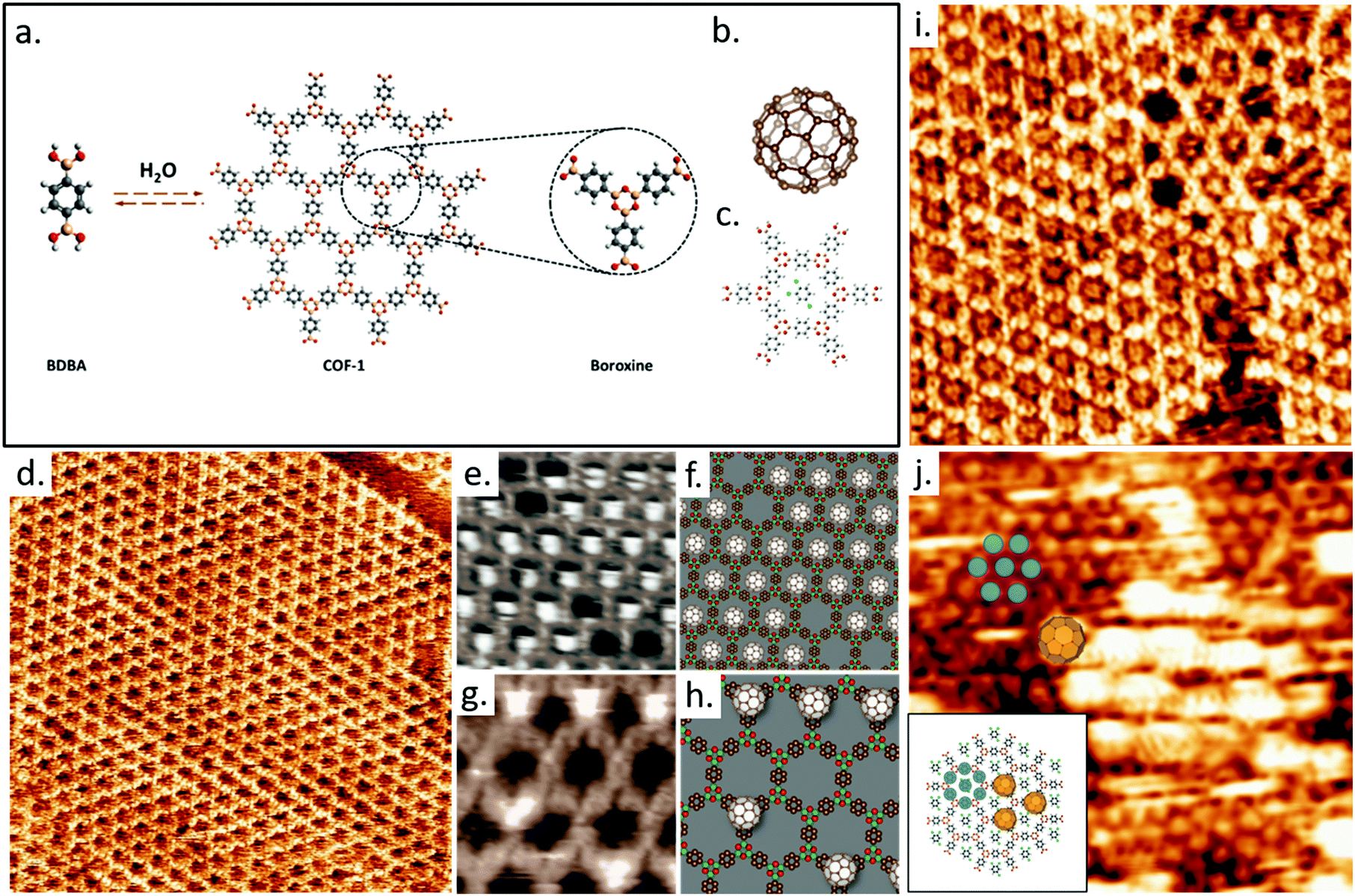 | ||
| Fig. 3 (a) The schematic illustration of self-condensation of BDBA monomers giving rise to 2D COF-1 template wherein defects can be recovered through the reversible reaction by offering excess water. A boroxine ring together with three neighbor benzenes is shown. (b) The molecular structure of C60. (c) DFT-optimized structure of one TCB solvent molecule in the hexagonal pore (M06-2X/LANL2DZ). (d) STM image showing the as-synthesized COF-1 on HOPG. Image area: 60.0 × 60.0 nm2. Tunneling conditions: V = −800 mV, I = 100 pA. STM images in (e) and (g) show the observed pore-site and top-site fullerene adsorption geometries, respectively. (f) and (h) are the proposed models for these adsorption sites. Image area: (e) 5.3 × 4.3 nm2, (g) 7.7 × 7.7 nm2. Tunneling conditions. V = −800 mV and I =100 pA. (i) COF-1 STM image showing the grain boundary consisting of pentagonal and heptagonal rings, connecting two domains rotated by 30 ± 1° with respect to one another. The image was collected at the interface of TCB and HOPG. Image area: 15.0 × 15.0 nm2. Tunneling conditions: V = −1000 mV, I = 100 pA. (j) Top-site selective population in the C60/COF-1 system. Image area: 15.0 × 15.0 nm2. Tunneling conditions: V = −800 mV, I = 100 pA. The inset image schematically shows top-site selective formation in C60/COF-1 system. The shaded blue circles over benzene rings represent the closed packed background in the STM image. Top-site C60 molecules are placed over boroxine rings, corresponding to the large bright spots in STM image. Images (a)–(h) have been adapted from ref. 87 with permission from the Royal Society for Chemistry, and images (i) and (j) are from ref. 111, published by the Royal Society of Chemistry. | ||
COF-1 can be synthesized from a different solvent molecule, such as 1,2,4-trichlorobenzene (TCB). The obtained surface-confined COF-1 template is qualitatively identical to that synthesized with heptanoic acid as solvent (Fig. 3i). At the TCB/HOPG interface, STM images reveal the adsorption of TCB in the hexagonal pores of COF-1 template. Gas-phase DFT simulations suggest that the adsorption of TCB in the hexagonal pore is stabilized through Cl⋯H hydrogen bonding interactions (Fig. 3c). The nucleophilic belt of the chlorine atoms in the TCB molecule orthogonal to the covalent bond presents higher electron density and negative electrostatic potential, which can form X⋯H hydrogen bonds with neighbouring hydrogen atoms on the COF-1 backbone. However, the interaction between the σ-hole of chlorine and nucleophilic oxygen atom of the COF-1 is screened by the hydrogens on the phenyl rings.
The presence of defects allowed us to investigate how this type of molecular sorting is affected by anomalies in the host lattice. A well-defined loop boundary consisting of a chain of pentagonal and heptagonal pores separates two different epitaxial domain orientations of COF-1 (Fig. 3i). The topological and pore size dependence of guest molecule adsorption is clear from these images: pores of different sizes can adsorb different numbers of TCB molecules. There is no adsorption of TCB in pentagonal rings but two TCB molecules adsorb simultaneously in the heptagonal pore. The observation of a different number of guest molecules adsorbed in different pore sizes is consistent with the commensurability of host and guest molecules, suggesting that both geometrical and size effects are important in binding the TCB.
The adsorption of solvent molecules in the host lattice can be used to control the adsorbed site of guest molecules.111 Fullerenes adsorb on the top-site of COF-1 (Fig. 3j) when both C60 and TCB are present at the TCB/HOPG interface since the pore-site is blocked by the adsorption of TCB molecule. These results suggest that surface-supported 2D porous COFs can selectively bind different molecules at specific sites and may offer a powerful platform for the recognition and patterning of guest molecules.
Combined solvent/template effects can also play a critical role in the formation of more complex assemblies, such as in the case where 2D COF-1 can be used to template solution-processed C60 guest molecules to form solvent-dependent structural arrangements and morphologies via a 2D to 3D growth process.35 Starting from a monolayer of T-layer C60, the first raised layer (R1) of adsorbed fullerenes forms a template-defined close packed structure when TCB is used as solvent. In contrast, a range of lower density architectures that deviate from the template-defined close packing are observed in heptanoic acid. In the case of heptanoic acid, the R1 C60 molecules can shift in two distinct geometries with respect to a given top-site C60, denoted as A-pattern shift and B-pattern shift, each of which exists in three-fold symmetry. DFT simulations suggest that A- and B-shift are stable structures, with the binding energy of the R1 fullerene calculated as EA = −0.21 eV and EB = −0.25 eV respectively.
The observed shifted C60 motifs can be attributed to the effect of co-adsorption of heptanoic acid molecules in the void spaces between C60 molecules in the T layer. When adsorbed in an upright orientation, heptanoic acid sterically inhibits the formation of the close-packed fullerene structure. This contrasts the inclusion which is instead allowed by the planar, pore-confined TCB solvent molecules. Without the COF-1 template, C60 molecules crystallize into a standard-FCC C60 close packed crystal on HOPG, rather than forming pseudopolymorphic phases incorporating heptanoic acid. This suggests that the co-adsorption of solvent molecules in the C60 film is driven by the template. These results suggest a pathway towards using the combination of 2D template and solvent effects to precisely control molecular self-assembly into the third dimension.
Responsive host/guest networks
Besides those host/guest systems with the rigid template network offering permanent porosities, the host can also be a flexible lattice, undergoing conformational transitions to accommodate guest molecules at the solid/liquid interface. The responsive changes of such template can provide a high guest selectivity, like bioenzymes, which can recognize their target substance through an induced fit mechanism.112 While responsive networks are usually probed through the sequential introduction of host and guest molecules, the simultaneous presence of guest with host molecules can also preferentially direct the formation of porous template structures to alternative close packed networks.113 However, stimulus-response-type studies are more common, and hence are our focus here.Nonporous molecular self-assembled structures can be transformed to a honeycomb porous network at the solution/solid interface through the addition of guest molecules. This has proven to facilitate a selective response to only planar guests with π-conjugated moieties.114 Simulation with different guest molecules can induce the template to form distinct host–guest surface patterns. For example, TMA honeycomb networks can adaptively reorganize upon the inclusion of the guest molecules with different core sizes but similar peripheral groups, resulting in a trihexagonal kagomé lattice or triangular patterns.115
We previously studied the self-assembly of biphenyl-3,4′,5-tricarboxylic acid (H3BHTC), which transforms from a low-porosity, low-symmetry network into a high symmetry, high-porosity host/guest lattice in response to the addition of coronene guest molecules at the solution/HOPG interface.116 Compared with TMA, H3BHTC has a reduced symmetry of C2v rather than C3 (Fig. 4a). It assembles into an offset interdigitated zigzag oblique structure with unit cell parameters a = (1.67 ± 0.05) nm, b = (1.93 ± 0.05) nm, and γ = (97° ± 3°), as shown in Fig. 4g and i. Gas-phase DFT simulations suggests that the lattice is stabilized by two types of dimeric hydrogen bonding associations, i.e., C–H⋯O cyclic dimer (Fig. 4c) and O–H⋯O zigzag dimer (Fig. 4d). Compared with a fully dimerically bonded lattice, the presented offset zigzag chain structure increases the surface molecular density, in favour of a higher number density of hydrogen bonds between the carboxylic groups. The offsetting of molecules can also invite solvent coadsorption within the pores, offering additional enthalpic stability. The introduction of coronene (Fig. 4b) to H3BHTC induces the formation of a highly-symmetric dimeric/trimeric (Fig. 4e and f) flower structure that incorporates two types of pores, as shown in Fig. 4h and j. The observed structure contains higher molecular density of H3BHTC and coronene, and the host/guest interactions are maximized since the cavities are better matched to coronene in both shape and size. This example shows the dramatic response that is possible from supramolecular system: not only does the porosity of the lattice respond to the addition of a stimulant molecule, the symmetry of the host lattice increases thanks to the presence of a high-symmetry guest.
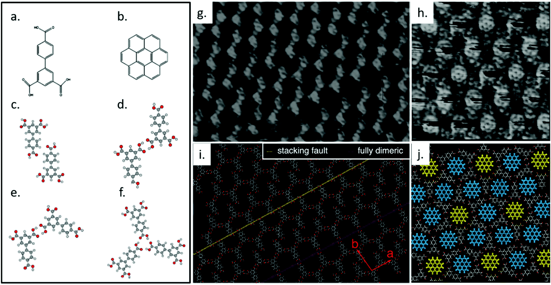 | ||
| Fig. 4 Molecular structures of H3BHTC (a) and coronene (b). Calculated geometries for H3BHTC C–H⋯O cyclic dimer (c), H3BHTC O–H⋯O zigzag dimer (d), H3BHTC chicken wire O–H⋯O cyclic dimer (e), H3BHTC trimer (f). (g) A high-resolution STM image of self-assembled layer of H3BHTC on HOPG. Image area: 16.0 × 12.0 nm2. Tunneling conditions: V = −0.7 V, I = 139 pA. (h) STM image showing the lattice formed by H3BHTC with coronene present, in which a hexagonal arrangement of coronene is evident. Image area: 10.0 × 10.0 nm2. Tunneling conditions: V = −297 mV, I = 119 pA. (i) A tentative model for the region in (g), which is produced based on an offset zigzag chain model that can account for both the frequently observed stacking faults (indicated by a yellow dashed line) and the porous dimeric structures (indicated by a pink dashed line). The unit vectors for the offset zigzag structure are shown in red. (j) Proposed model for image (i). Two different pore types can be identified that correspond to either a well-defined (fully dimeric pore, yellow coronene molecules) or streaked (dimeric/trimeric pore, blue coronene molecule) contrast on the coronene molecules. Adapted from ref. 116. Copyright 2014 American Chemical Society. | ||
Noncovalent modification of 2D materials
The rapid growth of the field of 2D materials117 has created an emerging opportunity for solution-processed molecular films: physisorbed films of electron accepting or donating small molecules can be used as a rapid, scalable approach towards the electronic modification of these systems.118 Electronic studies of the band structure modification due to molecular adsorption on graphene have largely focused on vacuum-deposited layers, although adsorption of the electron acceptor tetrafluoro-tetracyanoquinodimethane (F4-TCNQ), which produces p-type doping in graphene on SiC,119 shows similar doping whether the molecule is vacuum-deposited or solution-deposited,120 although in the latter case angle-resolved photoemission (ARPES) studies revealed residual contamination attributed to the solvent. However, this field is poised for growth, and solution/solid STM could make a significant contribution to understanding how solution deposition of small molecules can be used for electronic modification of graphene and other 2D materials, since it can provide insight into both the molecular ordering and the retention of solvent molecules at the interface.In our own work, we studied the adsorption of TMA on graphite and graphene at the heptanoic acid/solid interface.69 Adsorption of TMA on graphene has been theoretically predicted to modify its electronic structure;121 however, using ultraviolet photoemission spectroscopy (UPS), we were unable to identify changes to the valence band that could be clearly attributed to the TMA adsorption in the case of dried, solution-processed films. This is perhaps not surprising, since solvent coadsorption of fatty acid solvents is frequently observed in the porous molecular networks formed by TMA-like molecules at the solution/solid interface,22 and retained heptanoic acid could potentially obscure the effect of the TMA. Zhou et al., used transistor measurements to characterize the electronic modification made to graphene by a TMA layer deposited from 1-octatonic acid.122 While they were able to successfully measure a p-type doping of the graphene, they also noted a reduced mobility that they attributed to impurity-related scattering originating from the molecular layer. The authors suggest that this could relate to domain boundaries or point defects, but presumably retained solvent would also contribute to this scattering. The effect of using octanoic acid as a solvent for molecular deposition onto graphene-based devices was also noted by Zhang et al., who found that control devices fabricated using only octanoic acid, which was the solvent for the bis-urea-terthiophene (T3) deposition in their molecular devices, exhibited modifications to doping and mobility comparable to the T3-based devices.123 Overall, we suggest that solvent effects should be carefully considered in solution processing of films for electronic modification of 2D materials, and that the low-volatility solvents favoured for solution/solid STM may need to be used cautiously in the fabrication of films for molecular doping.
For electronic modification, long, linear molecules may offer a more promising route than small aromatics for solution-processed electronic modification layers; they have already been shown to be good candidates for chemical functionalization of 2D materials,124,125 and descriptions of electronic modifications are emerging.126 For example, the alkane n-hexatriacontane (HTC, C36H74) crystallizes into well-defined films on graphene, and the presence of a HTC film on a graphene filed effect transistor (FET) improved hole mobility from 17![[thin space (1/6-em)]](https://www.rsc.org/images/entities/char_2009.gif) 000 cm2 V−1 s−1 (without HTC) to 38000 cm2 V−1 s−1, an effect attributed to a reduction in charge density inhomogeneity arising from local lifting of the graphene by the HTC film.127 This mobility improvement was also observed for HTC on MoS2, suggesting that it might be a general approach for improving carrier mobilities in 2D materials. For both graphene and MoS2, solution/solid STM has long been used to study the adsorption of alkanes,128 and could continue to be a useful tool as studies progress towards other substrates and increasingly complex functionalized molecules. This complexity is can be critical for functionality: Le Liepvre and coworkers recently used solution/solid STM to optimize the self-assembly of a fluorescent supramolecular system made from a custom-designed 3D Janus tecton.129 In this case, the Janus tecton serves to hold the florescent moiety away from the graphene surface, preventing substrate-related quenching of the optical excitation.
000 cm2 V−1 s−1 (without HTC) to 38000 cm2 V−1 s−1, an effect attributed to a reduction in charge density inhomogeneity arising from local lifting of the graphene by the HTC film.127 This mobility improvement was also observed for HTC on MoS2, suggesting that it might be a general approach for improving carrier mobilities in 2D materials. For both graphene and MoS2, solution/solid STM has long been used to study the adsorption of alkanes,128 and could continue to be a useful tool as studies progress towards other substrates and increasingly complex functionalized molecules. This complexity is can be critical for functionality: Le Liepvre and coworkers recently used solution/solid STM to optimize the self-assembly of a fluorescent supramolecular system made from a custom-designed 3D Janus tecton.129 In this case, the Janus tecton serves to hold the florescent moiety away from the graphene surface, preventing substrate-related quenching of the optical excitation.
De Feyter's group recently combined solution/solid STM with Raman spectroscopy and electrical measurements to show that aliphatic amines with different lengths can be used to control the electronic characteristics of graphene devices.126 Orgiu, Samorì and coworkers have also used alkyl-based molecules to modify the electronic structure of graphene, specifically capitalizing on the predictable adsorption of the alkyl to create a 1D periodic modulation of potential through the inclusion of headgroups designed to induce an electric field due to a molecular dipole.2 In this case, the molecule shown in Fig. 5a induced an effect similar to the HTC films, producing an increase in carrier mobility, whereas the stronger electronic modulation introduced by the molecule shown in Fig. 5b caused a significant shift in the charge neutrality point. In follow-up work, the authors suggested that this approach might provide a general route to the modulation of electronic properties in vdW heterostructures formed from 2D materials, since the process is straightforward, scalable, and can be used for flexible architectures. They proposed that this type of non-covalent functionalization could introduce periodic potentials that significantly alter the electronic and optical properties of 2D vdW heterostructures, allowing for additional customization of these already modular materials.131
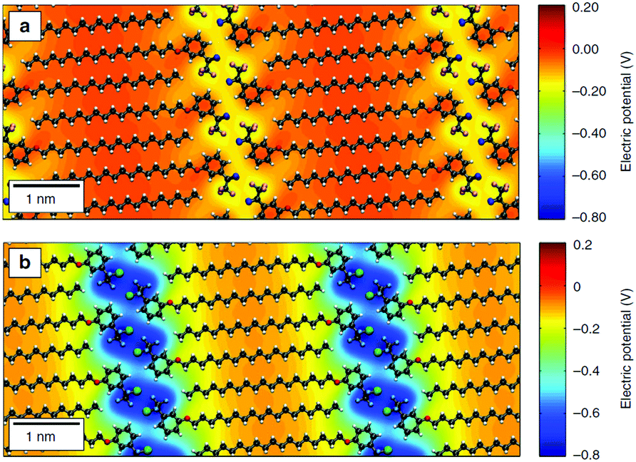 | ||
| Fig. 5 Differential electrical potential associated with linear molecules designed for self-assembly on 2D materials. The molecules incorporate long alky tails to ensure adsorption, aligning headgroups tailored for intermolecular interaction and electronic properties into well-defined 1D lamella. In the diagrams, grey atoms are carbon, white are hydrogen, red are nitrogen, light blue are fluorine and green chlorine. (a) shows a molecule called MBB-1 whereas (b) shows the molecule MBB-2; detailed descriptions of the molecules are available in the original paper. This figure has been reproduced from ref. 130, which was published under a Creative Commons license. | ||
Finally, we note that a range of novel opportunities also exist for the use of photoresponsive supramolecular assemblies on 2D materials, which can allow for optical modulation of the properties of the organic/2D material system.132
Conclusions/outlook
Alongside its important role in elucidating fundamental physical processes at surfaces, solution/solid STM has demonstrated its effectiveness as an enabling technology for imaging functional molecular materials. STM can provide a molecular-scale view of surface-confined assemblies, providing unique insights on structure and dynamic processes, and elucidating minority phases and aperiodic structures that are difficult or impossible to probe with other (surface-averaged) techniques. STM at the solution/solid interface has provided a view into a range of applications-relevant molecular systems, from self-assembled donor/acceptor networks with nanoscale periodicity to complex architectures that push the boundaries of programmed molecular recognition. The emerging need for novel, scalable approaches to electronic structure engineering in 2D materials highlights a growth area where solution/solid STM is poised to have a major impact. This imaging approach could also become useful to characterize the elusive interface between metal electrode, organic thin film and gate oxide in organic electronic devices. This structure of this interface largely determines charge injection and charge collection processes, which in turn underpin device performance.133In addition to the applications highlighted in this Article, the ability of STM to induce molecular reactions134 and modify surfaces positions it uniquely as a nanoscale fabrication device, and certain approaches to tip-induced nanopatterning are wholly dependent on implementation at the solution/solid interface. For example, in De Feyter's nanoshaving processes,135,136 the STM tip is used to selectively denude regions of a surface-confined molecular film, which is then repopulated with molecules from the overlying solution droplet. The introduction of a second molecular species, with nanometer precision, creates an opportunity for novel engineered materials, and demonstrates a potential pathway through which STM could realistically expand from a characterization instrument to a fabrication technology.
Conflicts of interest
There are no conflicts to declare.Acknowledgements
J. M. M. acknowledges funding support from the Australian Research Council (DE170101170). F. R. is grateful to the Canada Research Chair for funding and partial salary support and also acknowledges NSERC for a Discovery Grant, Sichuan province for a 1000 talent short term award and the Government of China for a short term Chang Jiang scholar award.Notes and references
- B. Voigtländer, Scanning Probe Microscopy, Springer, 2016 Search PubMed.
- F. Besenbacher, M. Brorson, B. S. Clausen, S. Helveg, B. Hinnemann, J. Kibsgaard, J. V. Lauritsen, P. G. Moses, J. K. Nørskov and H. Topsøe, Catal. Today, 2008, 130, 86–96 CrossRef.
- Ø. Fischer, M. Kugler, I. Maggio-Aprile, C. Berthod and C. Renner, Rev. Mod. Phys., 2007, 79, 353 CrossRef.
- Y. S. Hor, A. J. Williams, J. G. Checkelsky, P. Roushan, J. Seo, Q. Xu, H. W. Zandbergen, A. Yazdani, N. Ong and R. J. Cava, Phys. Rev. Lett., 2010, 104, 057001 CrossRef PubMed.
- Y. Zhang, K. He, C.-Z. Chang, C.-L. Song, L.-L. Wang, X. Chen, J.-F. Jia, Z. Fang, X. Dai, W.-Y. Shan, S.-Q. Shen, Q. Niu, X.-L. Qi, S.-C. Zhang, X.-C. Ma and Q.-K. Xue, Nat. Phys., 2010, 6, 584 Search PubMed.
- D. M. Cyr, B. Venkataraman and G. W. Flynn, Chem. Mater., 1996, 8, 1600–1615 CrossRef.
- S. De Feyter and F. C. De Schryver, Chem. Soc. Rev., 2003, 32, 139–150 RSC.
- S. De Feyter and F. C. De Schryver, J. Phys. Chem. B, 2005, 109, 4290–4302 CrossRef PubMed.
- A. G. Slater, P. H. Beton and N. R. Champness, Chem. Sci., 2011, 2, 1440–1448 RSC.
- J. A. Theobald, N. S. Oxtoby, M. A. Phillips, N. R. Champness and P. H. Beton, Nature, 2003, 424, 1029 CrossRef PubMed.
- O. Ivasenko and D. F. Perepichka, Chem. Soc. Rev., 2011, 40, 191–206 RSC.
- J. V. Barth, J. Weckesser, C. Cai, P. Günter, L. Bürgi, O. Jeandupeux and K. Kern, Angew. Chem., Int. Ed., 2000, 39, 1230–1234 CrossRef PubMed.
- R. Gutzler, O. Ivasenko, C. Fu, J. L. Brusso, F. Rosei and D. F. Perepichka, Chem. Commun., 2011, 47, 9453–9455 RSC.
- J. K. Yoon, W.-j. Son, K.-H. Chung, H. Kim, S. Han and S.-J. Kahng, J. Phys. Chem. C, 2011, 115, 2297–2301 CrossRef.
- F. Silly, J. Phys. Chem. C, 2013, 117, 20244–20249 CrossRef.
- Q.-N. Zheng, X.-H. Liu, T. Chen, H.-J. Yan, T. Cook, D. Wang, P. J. Stang and L.-J. Wan, J. Am. Chem. Soc., 2015, 137, 6128–6131 CrossRef PubMed.
- D. Bléger, D. Kreher, F. Mathevet, A. J. Attias, G. Schull, A. Huard, L. Douillard, C. Fiorini-Debuischert and F. Charra, Angew. Chem., 2007, 119, 7548–7551 CrossRef.
- J. P. Rabe and S. Buchholz, Phys. Rev. Lett., 1991, 66, 2096 CrossRef PubMed.
- Y. Xue and M. B. Zimmt, Chem. Commun., 2011, 47, 8832–8834 RSC.
- Y. Hu, K. Miao, L. Xu, X. Miao and W. Deng, J. Phys. Chem. C, 2017, 121, 21449–21460 CrossRef.
- J. M. MacLeod and F. Rosei, Aust. J. Chem., 2011, 64, 1299–1300 CrossRef.
- Y. Yang and C. Wang, Curr. Opin. Colloid Interface Sci., 2009, 14, 135–147 CrossRef.
- Y. Yang and M. B. Zimmt, J. Phys. Chem. B, 2015, 119, 7740–7748 CrossRef PubMed.
- U. Mazur and K. Hipps, Chem. Commun., 2015, 51, 4737–4749 RSC.
- K. Hipps and U. Mazur, Langmuir, 2018, 34, 3–17 CrossRef PubMed.
- W. Song, N. Martsinovich, W. Heckl and M. Lackinger, Chem. Commun., 2014, 50, 13465–13468 RSC.
- W. Song, N. Martsinovich, W. M. Heckl and M. Lackinger, J. Am. Chem. Soc., 2013, 135, 14854–14862 CrossRef PubMed.
- J. M. MacLeod, J. Lipton-Duffin, C. Fu, T. Taerum, D. F. Perepichka and F. Rosei, ACS Nano, 2017, 11, 8901–8909 CrossRef PubMed.
- J. R. Reimers, D. Panduwinata, J. Visser, Y. Chin, C. Tang, L. Goerigk, M. J. Ford, M. Sintic, T.-J. Sum, M. J. Coenen, B. L. M. Hendriksen, J. A. A. Elemans, N. S. Hush and M. J. Crossley, Proc. Natl. Acad. Sci. U. S. A., 2015, 112, E6101–E6110 CrossRef PubMed.
- S. Conti and M. Cecchini, Phys. Chem. Chem. Phys., 2016, 18, 31480–31493 RSC.
- J. A. Münninghoff and J. A. Elemans, Chem. Commun., 2017, 53, 1769–1788 RSC.
- S. Claridge, Chem. Commun., 2018, 54, 6681–6691 RSC.
- K. Iritani, K. Tahara, S. De Feyter and Y. Tobe, Langmuir, 2017, 33, 4601–4618 CrossRef PubMed.
- R. Gatti, J. M. MacLeod, J. A. Lipton-Duffin, A. G. Moiseev, D. F. Perepichka and F. Rosei, J. Phys. Chem. C, 2014, 118, 25505–25516 CrossRef.
- D. Cui, M. Ebrahimi, F. Rosei and J. M. Macleod, J. Am. Chem. Soc., 2017, 139, 16732–16740 CrossRef PubMed.
- S.-L. Lee, Z. Yuan, L. Chen, K. S. Mali, K. Müllen and S. De Feyter, J. Am. Chem. Soc., 2014, 136, 7595–7598 CrossRef PubMed.
- O. V. Mikhnenko, P. W. Blom and T.-Q. Nguyen, Energy Environ. Sci., 2015, 8, 1867–1888 RSC.
- Y. Huang, E. J. Kramer, A. J. Heeger and G. C. Bazan, Chem. Rev., 2014, 114, 7006–7043 CrossRef PubMed.
- C. Liu, Y. Xu and Y.-Y. Noh, Mater. Today, 2015, 18, 79–96 CrossRef.
- S. S. Cheng, P. Y. Huang, M. Ramesh, H. C. Chang, L. M. Chen, C. M. Yeh, C. L. Fung, M. C. Wu, C. C. Liu, C. Kim, H.-C. Lin, M.-C. Chen and C.-W. Chu, Adv. Funct. Mater., 2014, 24, 2057–2063 CrossRef.
- S. Slim and F. Rosei, Science, 2016, 353, 1098–1099 CrossRef PubMed.
- F. So, Organic Electronics: Materials, Processing, Devices and Applications, CRC Press, 2009 Search PubMed.
- C. J. Brabec, S. Gowrisanker, J. J. Halls, D. Laird, S. Jia and S. P. Williams, Adv. Mater., 2010, 22, 3839–3856 CrossRef PubMed.
- J. Zhang, Y. Zhang, J. Fang, K. Lu, Z. Wang, W. Ma and Z. Wei, J. Am. Chem. Soc., 2015, 137, 8176–8183 CrossRef PubMed.
- L. Xu, L. Yang and S. Lei, Nanoscale, 2012, 4, 4399–4415 RSC.
- J. Miwa, F. Cicoira, J. Lipton-Duffin, D. Perepichka, C. Santato and F. Rosei, Nanotechnology, 2008, 19, 424021 CrossRef PubMed.
- J. A. Miwa, F. Cicoira, S. Bedwani, J. Lipton-Duffin, D. F. Perepichka, A. Rochefort and F. Rosei, J. Phys. Chem. C, 2008, 112, 10214–10221 CrossRef.
- B. Lu, T. Iimori, K. Sakamoto, K. Nakatsuji, F. Rosei and F. Komori, J. Phys. Chem. C, 2008, 112, 10187–10192 CrossRef.
- L. F. Dössel, V. Kamm, I. A. Howard, F. D. R. Laquai, W. Pisula, X. Feng, C. Li, M. Takase, T. Kudernac, S. De Feyter and K. Müllen, J. Am. Chem. Soc., 2012, 134, 5876–5886 CrossRef PubMed.
- N. Tchebotareva, X. Yin, M. D. Watson, P. Samorì, J. P. Rabe and K. Müllen, J. Am. Chem. Soc., 2003, 125, 9734–9739 CrossRef PubMed.
- P. Samorì, X. Yin, N. Tchebotareva, Z. Wang, T. Pakula, F. Jäckel, M. D. Watson, A. Venturini, K. Müllen and J. P. Rabe, J. Am. Chem. Soc., 2004, 126, 3567–3575 CrossRef PubMed.
- P. Samorì, A. Fechtenkötter, E. Reuther, M. D. Watson, N. Severin, K. Müllen and J. P. Rabe, Adv. Mater., 2006, 18, 1317–1321 CrossRef.
- J. M. Mativetsky, M. Kastler, R. C. Savage, D. Gentilini, M. Palma, W. Pisula, K. Müllen and P. Samori, Adv. Funct. Mater., 2009, 19, 2486–2494 CrossRef.
- Y. Hu, L. F. Dössel, X.-Y. Wang, S. Mahesh, W. Pisula, S. De Feyter, X. Feng, K. Müllen and A. Narita, ChemPlusChem, 2017, 82, 1030–1033 CrossRef.
- E. Mena-Osteritz and P. Bäuerle, Adv. Mater., 2006, 18, 447–451 CrossRef.
- J. M. MacLeod, O. Ivasenko, C. Fu, T. Taerum, F. Rosei and D. F. Perepichka, J. Am. Chem. Soc., 2009, 131, 16844–16850 CrossRef PubMed.
- L. Piot, F. Silly, L. Tortech, Y. Nicolas, P. Blanchard, J. Roncali and D. Fichou, J. Am. Chem. Soc., 2009, 131, 12864–12865 CrossRef PubMed.
- M. O. Blunt, J. C. Russell, M. del Carmen Gimenez-Lopez, N. Taleb, X. Lin, M. Schröder, N. R. Champness and P. H. Beton, Nat. Chem., 2011, 3, 74 CrossRef PubMed.
- H. Ouchi, X. Lin, T. Kizaki, D. D. Prabhu, F. Silly, T. Kajitani, T. Fukushima, K.-I. Nakayama and S. Yagai, Chem. Commun., 2016, 52, 7874–7877 RSC.
- S. Yagai, M. Suzuki, X. Lin, M. Gushiken, T. Noguchi, T. Karatsu, A. Kitamura, A. Saeki, S. Seki, Y. Kikkawa, Y. Tani and K. Nakayama, Chem. – Eur. J., 2014, 20, 16128–16137 CrossRef PubMed.
- X. Lin, M. Suzuki, M. Gushiken, M. Yamauchi, T. Karatsu, T. Kizaki, Y. Tani, K.-I. Nakayama, M. Suzuki, H. Yamada, T. Kajitani, T. Fukushima, Y. Kikkawa and S. Yagai, Sci. Rep., 2017, 7, 43098 CrossRef PubMed.
- R. Ruiz, D. Choudhary, B. Nickel, T. Toccoli, K.-C. Chang, A. C. Mayer, P. Clancy, J. M. Blakely, R. L. Headrick, S. Iannotta and G. G. Malliaras, Chem. Mater., 2004, 16, 4497–4508 CrossRef.
- X. Bai, K. Zong, J. Ly, J. S. Mehta, M. Hand, K. Molnar, S. Lee, B. Kahr, J. M. Mativetsky, A. Briseno and S. S. Lee, Chem. Mater., 2017, 29, 7571–7578 CrossRef.
- J. Yang, D. Yan and T. S. Jones, Chem. Rev., 2015, 115, 5570–5603 CrossRef PubMed.
- S. Izawa, K. Nakano, K. Suzuki, Y. Chen, T. Kikitsu, D. Hashizume, T. Koganezawa, T.-Q. Nguyen and K. Tajima, Sci. Rep., 2018, 8, 481 CrossRef PubMed.
- A. O. Jones, B. Chattopadhyay, Y. H. Geerts and R. Resel, Adv. Funct. Mater., 2016, 26, 2233–2255 CrossRef.
- W. H. Lee, J. Park, S. H. Sim, S. Lim, K. S. Kim, B. H. Hong and K. Cho, J. Am. Chem. Soc., 2011, 133, 4447–4454 CrossRef PubMed.
- H. Ying Mao, R. Wang, Y. Wang, T. Chao Niu, J. Qiang Zhong, M. Yang Huang, D. Chen Qi, K. Ping Loh, A. Thye Shen Wee and W. Chen, Appl. Phys. Lett., 2011, 99, 180 CrossRef.
- J. MacLeod, J. Lipton-Duffin, D. Cui, S. De Feyter and F. Rosei, Langmuir, 2015, 31, 7016–7024 CrossRef PubMed.
- T. Wang, T. R. Kafle, B. Kattel, Q. Liu, J. Wu and W.-L. Chan, Sci. Rep., 2016, 6, 28895 CrossRef PubMed.
- C. Fu, H.-p. Lin, J. M. Macleod, A. Krayev, F. Rosei and D. F. Perepichka, Chem. Mater., 2016, 28, 951–961 CrossRef.
- E. Bauer, Z. Kristallogr. - Cryst. Mater., 1958, 110, 395–431 CrossRef.
- R. Gutzler, C. Fu, A. Dadvand, Y. Hua, J. M. MacLeod, F. Rosei and D. F. Perepichka, Nanoscale, 2012, 4, 5965–5971 RSC.
- O. Fenwick, C. Van Dyck, K. Murugavel, D. Cornil, F. Reinders, S. Haar, M. Mayor, J. Cornil and P. Samorì, J. Mater. Chem. C, 2015, 3, 3007–3015 RSC.
- F. Cicoira, C. Santato and F. Rosei, Top. Curr. Chem., 2008, 285, 203–267 CrossRef PubMed.
- F. Cicoira and F. Rosei, Surf. Sci., 2006, 600, 1–5 CrossRef.
- J. M. Lehn, Angew. Chem., Int. Ed. Engl., 1988, 27, 89–112 CrossRef.
- F. Zeng and S. C. Zimmerman, Chem. Rev., 1997, 97, 1681–1712 CrossRef PubMed.
- D. J. Cram, Angew. Chem., Int. Ed. Engl., 1988, 27, 1009–1020 CrossRef.
- J. M. Lehn, Angew. Chem., Int. Ed. Engl., 1990, 29, 1304–1319 CrossRef.
- J. Teyssandier, S. De Feyter and K. S. Mali, Chem. Commun., 2016, 52, 11465–11487 RSC.
- P. Samorì, J. Mater. Chem., 2004, 14, 1353–1366 RSC.
- B. Li, K. Tahara, J. Adisoejoso, W. Vanderlinden, K. S. Mali, S. De Gendt, Y. Tobe and S. De Feyter, ACS Nano, 2013, 7, 10764–10772 CrossRef PubMed.
- Y. Xue and M. B. Zimmt, J. Am. Chem. Soc., 2012, 134, 4513–4516 CrossRef PubMed.
- K. G. Nath, O. Ivasenko, J. A. Miwa, H. Dang, J. D. Wuest, A. Nanci, D. F. Perepichka and F. Rosei, J. Am. Chem. Soc., 2006, 128, 4212–4213 CrossRef PubMed.
- K. G. Nath, O. Ivasenko, J. M. MacLeod, J. A. Miwa, J. D. Wuest, A. Nanci, D. F. Perepichka and F. Rosei, J. Phys. Chem. C, 2007, 111, 16996–17007 CrossRef.
- D. Cui, J. MacLeod, M. Ebrahimi, D. Perepichka and F. Rosei, Chem. Commun., 2015, 51, 16510–16513 RSC.
- J.-Y. Gu, Z.-F. Cai, D. Wang and L.-J. Wan, ACS Nano, 2016, 10, 8746–8750 CrossRef PubMed.
- D. Mandler and S. Kraus-Ophir, J. Solid State Electrochem., 2011, 15, 1535 CrossRef.
- K. Ariga, H. Ito, J. P. Hill and H. Tsukube, Chem. Soc. Rev., 2012, 41, 5800–5835 RSC.
- D. Bonifazi, S. Mohnani and A. Llanes-Pallas, Chem. – Eur. J., 2009, 15, 7004–7025 CrossRef PubMed.
- M. Li, K. Deng, S. B. Lei, Y. L. Yang, T. S. Wang, Y. T. Shen, C. R. Wang, Q. D. Zeng and C. Wang, Angew. Chem., 2008, 120, 6819–6823 CrossRef.
- K. Tahara, K. Nakatani, K. Iritani, S. De Feyter and Y. Tobe, ACS Nano, 2016, 10, 2113–2120 CrossRef PubMed.
- J. Adisoejoso, K. Tahara, S. Okuhata, S. Lei, Y. Tobe and S. De Feyter, Angew. Chem., 2009, 121, 7489–7493 CrossRef.
- E. Ghijsens, H. Cao, A. Noguchi, O. Ivasenko, Y. Fang, K. Tahara, Y. Tobe and S. De Feyter, Chem. Commun., 2015, 51, 4766–4769 RSC.
- K. Tahara, K. Katayama, M. O. Blunt, K. Iritani, S. De Feyter and Y. Tobe, ACS Nano, 2014, 8, 8683–8694 CrossRef PubMed.
- S. Lei, K. Tahara, X. Feng, S. Furukawa, F. C. De Schryver, K. Müllen, Y. Tobe and S. De Feyter, J. Am. Chem. Soc., 2008, 130, 7119–7129 CrossRef PubMed.
- K. Tahara, K. Inukai, J. Adisoejoso, H. Yamaga, T. Balandina, M. O. Blunt, S. De Feyter and Y. Tobe, Angew. Chem., Int. Ed., 2013, 52, 8373–8376 CrossRef PubMed.
- S. Lei, M. Surin, K. Tahara, J. Adisoejoso, R. Lazzaroni, Y. Tobe and S. D. Feyter, Nano Lett., 2008, 8, 2541–2546 CrossRef PubMed.
- G. Velpula, T. Takeda, J. Adisoejoso, K. Inukai, K. Tahara, K. S. Mali, Y. Tobe and S. De Feyter, Chem. Commun., 2017, 53, 1108–1111 RSC.
- S. J. Griessl, M. Lackinger, F. Jamitzky, T. Markert, M. Hietschold and W. M. Heckl, Langmuir, 2004, 20, 9403–9407 CrossRef PubMed.
- S. J. Griessl, M. Lackinger, F. Jamitzky, T. Markert, M. Hietschold and W. M. Heckl, J. Phys. Chem. B, 2004, 108, 11556–11560 CrossRef.
- G.-B. Pan, X.-H. Cheng, S. Höger and W. Freyland, J. Am. Chem. Soc., 2006, 128, 4218–4219 CrossRef PubMed.
- S. Stepanow, M. Lingenfelder, A. Dmitriev, H. Spillmann, E. Delvigne, N. Lin, X. Deng, C. Cai, J. V. Barth and K. Kern, Nat. Mater., 2004, 3, 229–233 CrossRef PubMed.
- T. Kudernac, S. Lei, J. A. Elemans and S. De Feyter, Chem. Soc. Rev., 2009, 38, 402–421 RSC.
- J. W. Colson and W. R. Dichtel, Nat. Chem., 2013, 5, 453–465 CrossRef PubMed.
- C. S. Diercks and O. M. Yaghi, Science, 2017, 355, eaal1585 CrossRef PubMed.
- A. P. Cote, A. I. Benin, N. W. Ockwig, M. O'Keeffe, A. J. Matzger and O. M. Yaghi, Science, 2005, 310, 1166–1170 CrossRef PubMed.
- J. r. F. Dienstmaier, A. M. Gigler, A. J. Goetz, P. Knochel, T. Bein, A. Lyapin, S. Reichlmaier, W. M. Heckl and M. Lackinger, ACS Nano, 2011, 5, 9737–9745 CrossRef PubMed.
- J. r. F. Dienstmaier, D. D. Medina, M. Dogru, P. Knochel, T. Bein, W. M. Heckl and M. Lackinger, ACS Nano, 2012, 6, 7234–7242 CrossRef PubMed.
- D. Cui, J. MacLeod, M. Ebrahimi and F. Rosei, CrystEngComm, 2017, 19, 4927–4932 RSC.
- A. M. Davis and S. J. Teague, Angew. Chem., Int. Ed., 1999, 38, 736–749 CrossRef PubMed.
- M. Blunt, X. Lin, M. del Carmen Gimenez-Lopez, M. Schröder, N. R. Champness and P. H. Beton, Chem. Commun., 2008, 2304–2306 RSC.
- S. Furukawa, K. Tahara, F. C. De Schryver, M. Van der Auweraer, Y. Tobe and S. De Feyter, Angew. Chem., 2007, 119, 2889–2892 CrossRef.
- Q.-N. Zheng, L. Wang, Y.-W. Zhong, X.-H. Liu, T. Chen, H.-J. Yan, D. Wang, J.-N. Yao and L.-J. Wan, Langmuir, 2014, 30, 3034–3040 CrossRef PubMed.
- J. M. MacLeod, Z. Ben Chaouch, D. F. Perepichka and F. Rosei, Langmuir, 2013, 29, 7318–7324 CrossRef PubMed.
- R. Mas-Balleste, C. Gomez-Navarro, J. Gomez-Herrero and F. Zamora, Nanoscale, 2011, 3, 20–30 RSC.
- B. Cai, S. Zhang, Z. Yan and H. Zeng, ChemNanoMat, 2015, 1, 542–557 CrossRef.
- W. Chen, S. Chen, D. C. Qi, X. Y. Gao and A. T. S. Wee, J. Am. Chem. Soc., 2007, 129, 10418–10422 CrossRef PubMed.
- C. Coletti, C. Riedl, D. S. Lee, B. Krauss, L. Patthey, K. von Klitzing, J. H. Smet and U. Starke, Phys. Rev. B: Condens. Matter Mater. Phys., 2010, 81, 235401 CrossRef.
- F. Shayeganfar and A. Rochefort, Langmuir, 2014, 30, 9707–9716 CrossRef PubMed.
- Q. Zhou, Y. Li, Q. Li, Y. Wang, Y. Yang, Y. Fang and C. Wang, Nanoscale, 2014, 6, 8387–8391 RSC.
- X. Zhang, E. H. Huisman, M. Gurram, W. R. Browne, B. J. van Wees and B. L. Feringa, Small, 2014, 10, 1735–1740 CrossRef PubMed.
- J. J. Bang, A. G. Porter, T. C. Davis, T. R. Hayes and S. A. Claridge, Langmuir, 2018, 34, 5454–5463 CrossRef PubMed.
- T. C. Davis, J. J. Bang, J. T. Brooks, D. G. McMillan and S. A. Claridge, Langmuir, 2018, 34, 1353–1362 CrossRef PubMed.
- R. Phillipson, C. J. L. de la Rosa, J. Teyssandier, P. Walke, D. Waghray, Y. Fujita, J. Adisoejoso, K. S. Mali, I. Asselberghs, C. Huyghebaert, H. Uji-i, S. De Gendt and S. De Feyter, Nanoscale, 2016, 8, 20017–20026 RSC.
- Y. J. Yu, G. H. Lee, J. I. Choi, Y. S. Shim, C. H. Lee, S. J. Kang, S. Lee, K. T. Rim, G. W. Flynn, J. Hone, Y.-H. Kim, P. Kim, C. Nuckolls and S. Ahn, Adv. Mater., 2017, 29, 1603925 CrossRef PubMed.
- L. C. Giancarlo, H. Fang, S. M. Rubin, A. A. Bront and G. W. Flynn, J. Phys. Chem. B, 1998, 102, 10255–10263 CrossRef.
- S. Le Liepvre, P. Du, D. Kreher, F. Mathevet, A.-J. Attias, C. Fiorini-Debuisschert, L. Douillard and F. Charra, ACS Photonics, 2016, 3, 2291–2296 CrossRef.
- M. Gobbi, S. Bonacchi, J. X. Lian, Y. Liu, X.-Y. Wang, M.-A. Stoeckel, M. A. Squillaci, G. D’Avino, A. Narita, K. Müllen, X.-L. Feng, Y. Olivier, D. Beljonne, P. Samorì and E. Orgiu, Nat. Commun., 2017, 8, 14767 CrossRef PubMed.
- M. Gobbi, E. Orgiu and P. Samorì, Adv. Mater., 2018, 30, 1706103 CrossRef PubMed.
- S. Wieghold, J. Li, P. Simon, M. Krause, Y. Avlasevich, C. Li, J. A. Garrido, U. Heiz, P. Samorì, K. Müllen, F. Esch, J. V. Barth and C.-A. Palma, Nat. Commun., 2016, 7, 10700 CrossRef PubMed.
- C. Santato and F. Rosei, Nat. Chem., 2010, 2, 344 CrossRef PubMed.
- J. M. MacLeod, J. Lipton-Duffin, C. Fu and F. Rosei, ACS Nano, 2009, 3, 3347–3351 CrossRef PubMed.
- L. Verstraete, J. Greenwood, B. E. Hirsch and S. De Feyter, ACS Nano, 2016, 10, 10706–10715 CrossRef PubMed.
- J. Plas, O. Ivasenko, N. Martsinovich, M. Lackinger and S. De Feyter, Chem. Commun., 2016, 52, 68–71 RSC.
| This journal is © The Royal Society of Chemistry 2018 |