
 Open Access Article
 This Open Access Article is licensed under a
 Creative Commons Attribution 3.0 Unported Licence
Spectroscopic and electrical signatures of acceptor states in solution processed Cu2ZnSn(S,Se)4 solar cells†‡
Devendra
Tiwari
 a,
Ekaterina
Skidchenko
bf,
Jake W.
Bowers
c,
Michael V.
Yakushev
bde,
Robert W.
Martin
b and
David J.
Fermin
*a
a,
Ekaterina
Skidchenko
bf,
Jake W.
Bowers
c,
Michael V.
Yakushev
bde,
Robert W.
Martin
b and
David J.
Fermin
*a
aSchool of Chemistry, University of Bristol, Bristol BS8 1TS, UK. E-mail: d.tiwari@bristol.ac.uk; david.fermin@bristol.ac.uk
bDepartment of Physics, SUPA, Strathclyde University, Glasgow G4 0NG, UK
cCentre for Renewable Energy Systems Technology (CREST), Wolfson School of Mechanical, Electrical and Manufacturing Engineering, Loughborough University, Loughborough LE11 3TU, UK
dInstitute of Metal Physics UB RAS, S. Kovalevskaya Street 18, 620990, Ekaterinburg, Russia
eUral Federal University, Mira 19, 620002 Ekaterinburg, Russia
fSkolkovo Institute of Science and Technology, Skolkovo Innovation Center, Nobelya str., Building 3, Moscow 143026, Russia
First published on 25th October 2017
Abstract
The nature and dynamics of acceptor states in solution-processed Cu2ZnSn(S,Se)4 (CZTSSe) thin films are investigated by variable temperature photoluminescence (PL) and electrical impedance spectroscopy. Highly pure I-4 phase CZTSSe with the composition Cu1.6ZnSn0.9(S0.23Se0.77)4 is synthesized by sequentially spin coating of dimethyl-formamide/isopropanol solutions containing metal salts and thiourea onto Mo coated glass, followed by annealing in an Se atmosphere at 540 °C. As-annealed films are highly compact with a thickness of 1.3 μm and grain sizes above 800 nm, with a band gap of 1.18 eV. Photovoltaic devices of 0.25 cm2 with the architecture glass/Mo/CZTSSe/CdS/i-ZnO/Al:ZnO demonstrate a power conversion efficiency reaching up to 5.7% in the absence of an anti-reflective coating. Under AM 1.5G illumination at 296 K, the best device shows a 396 mV open-circuit voltage (VOC), 27.8 mA cm−2 short-circuit current (JSC) and 52% fill factor (FF). The overall dispersion of these parameters is under 15% for a total of 20 devices. In the near IR region, PL spectra are dominated by two broad and asymmetrical bands at 1.14 eV (PL1) and 0.95 eV (PL2) with characteristic power and temperature dependences. Analysis of the device electrical impedance spectra also reveals two electron acceptor states with the same activation energy as those observed by PL. This allows assigning PL1 as a radiative recombination at localized copper vacancies (VCu), while PL2 is associated with CuZn antisites, broadened by potential fluctuations (band tails). The impact of these states on device performance as well as other parameters, such as barrier collection heights introduced by partial selenization of the back contact, are discussed.
Introduction
For the last 10 years, two new families of materials have dominated research efforts towards low-cost sustainable photovoltaic technologies, namely organo–inorganic hybrid lead perovskite and inorganic kesterites.1 Although perovskite laboratory-scale champion cell efficiencies have gone through an impressive improvement from 3.8% to over 22% in the last 8 years,2,3 long-term stability and technology scalability remain formidable challenges.3,4 Inorganic kesterites, in which Cu2ZnSn(S,Se)4 or CZTSSe is the most prominent example, are widely considered as replacements of the more mature Cu(In,Ga)Se2 (CIGS) technology which has reached cell efficiencies above 22%.5 Slower improvements of CZTSSe cell efficiencies in comparison to those of perovskites cells can partly be explained in terms of the vastly superior research efforts on the latter as reflected by the number of publications.6 In order to substantially improve kesterite cell performances, it is crucial to assess the nature and origin of recombination pathways.CZTSSe solar cells featuring a conversion efficiency above 10% have been fabricated using a variety of physical vapor deposition and non-vacuum deposition routes, demonstrating their synthetic flexibility.7,8 Even though kesterites structurally resemble CIGS, there are significant differences in terms of processing chemistry as well as the nature of the electronic and structural defects.7,9–11 For instance, studies suggest that CZTSSe is significantly more susceptible to deep point defects and interfacial trap states than CIGS.7,10–12 Computational studies have also predicted the presence of numerous point defects (vacancies and antisites) as well as the presence of secondary phases, including binary and ternary sulfides (e.g. Cu2SnS3).12 A variety of approaches have been reported to mitigate such structural defects, including the introduction of additives, as recently exemplified in our previous report.13
In the present study, we establish a link between the chemical nature of the defect sites in CZTSSe and how they manifest themselves in device properties by correlating the temperature dependences of photoluminescence and electrical impedance. CZTSSe thin-films are prepared by a solution based method followed by reactive annealing in the presence of Se. Quantitative structural and spectroscopic analysis confirmed the formation of a pure I-4 phase with a composition of Cu1.6ZnSn0.9(S0.23Se0.77)4. PL studies show two bands located at 1.14 eV (PL1) and 0.95 eV (PL2) with well-defined power and temperature dependences. Quantitative analysis shows that these sites are associated with acceptor states, most likely Cu-vacancies (PL1) and CuZn antisite clusters (PL2). Devices with the structure Mo/CZTSSe/CdS/i-ZnO/Al:ZnO, with power conversion efficiencies of up to 5.7% under an AM 1.5G illumination, were investigated by electrical impedance spectroscopy. Analysis of the impedance responses allowed identifying two time constants with similar activation energies of the PL responses. These studies link PL (chemically sensitive information) and electrical (device sensitive) responses, providing a key step toward understanding power conversion losses in these devices.
Experimental procedure
CZTSSe film deposition, device fabrication and measurements
CZTSSe films are deposited from a single solution precursor solution consisting of copper(II) chloride, zinc chloride, tin(II) chloride and thiourea dissolved in a 1![[thin space (1/6-em)]](https://www.rsc.org/images/entities/char_2009.gif) :1 solvent mixture of dimethyl formamide and isopropanol with a total metal concentration of 0.93 M. The precursor solution is spin-coated onto 5 × 5 cm2 Mo coated glass substrates and heated to 300 °C on a hotplate in air. This cycle is repeated 4 times to achieve the final thickness. These films are annealed in an Se atmosphere in a graphite box at 540 °C using a MTI-OTF1200X furnace. Differential scanning calorimetry data reported in our previous work demonstrated that CZTS crystallizes from a similar precursor formulation at 480 °C.13 Several reports have also shown that highly crystalline materials can be obtained upon annealing in the range of 450 to 550 °C.14 No blocking layers to prevent Na diffusion to CZTSSe or Se diffusion to Mo layer are employed. The annealed films are etched in 10% aq. KCN solution for 30 seconds and subsequently introduced in a chemical bath maintained at 70 °C consisting of CdSO4, thiourea and ammonium hydroxide for the CdS buffer layer deposition, following a protocol reported previously.15 i-ZnO and Al:ZnO transparent conducting oxide layers are deposited by RF-sputtering. No metal contact and anti-reflection coating is deposited in present case and Al:ZnO acts as the top contact. Cells with a total area of 0.25 cm2 are scribed mechanically. J–V characteristic of the devices are measured under simulated AM 1.5G from a class AAA solar simulator (Wacom, Japan) with an integrated power output of 100 mW cm−2 at 296 K. External quantum efficiencies (EQEs) of the devices are measured using a Bentham TM 300 monochromator (Bentham instruments) and illumination from Xe and halogen sources. A calibrated Si photodiode is used as the reference for J–V and EQE measurements. Low temperature PL measurements are performed using a custom made setup comprising a 514.5 nm Ar ion laser as the excitation source, a closed cycle liquid He cryostat for temperature variation, a 1 m focal length monochromator and a biased InGaAs photodetector for acquiring the spectrum. Low temperature impedance measurements are done in a modified Linkam HFS 600PB4 cooling stage and Solartron impedance analyzer in the frequency range of 1 Hz and 1 MHz with an AC potential modulation of 25 mV rms.
:1 solvent mixture of dimethyl formamide and isopropanol with a total metal concentration of 0.93 M. The precursor solution is spin-coated onto 5 × 5 cm2 Mo coated glass substrates and heated to 300 °C on a hotplate in air. This cycle is repeated 4 times to achieve the final thickness. These films are annealed in an Se atmosphere in a graphite box at 540 °C using a MTI-OTF1200X furnace. Differential scanning calorimetry data reported in our previous work demonstrated that CZTS crystallizes from a similar precursor formulation at 480 °C.13 Several reports have also shown that highly crystalline materials can be obtained upon annealing in the range of 450 to 550 °C.14 No blocking layers to prevent Na diffusion to CZTSSe or Se diffusion to Mo layer are employed. The annealed films are etched in 10% aq. KCN solution for 30 seconds and subsequently introduced in a chemical bath maintained at 70 °C consisting of CdSO4, thiourea and ammonium hydroxide for the CdS buffer layer deposition, following a protocol reported previously.15 i-ZnO and Al:ZnO transparent conducting oxide layers are deposited by RF-sputtering. No metal contact and anti-reflection coating is deposited in present case and Al:ZnO acts as the top contact. Cells with a total area of 0.25 cm2 are scribed mechanically. J–V characteristic of the devices are measured under simulated AM 1.5G from a class AAA solar simulator (Wacom, Japan) with an integrated power output of 100 mW cm−2 at 296 K. External quantum efficiencies (EQEs) of the devices are measured using a Bentham TM 300 monochromator (Bentham instruments) and illumination from Xe and halogen sources. A calibrated Si photodiode is used as the reference for J–V and EQE measurements. Low temperature PL measurements are performed using a custom made setup comprising a 514.5 nm Ar ion laser as the excitation source, a closed cycle liquid He cryostat for temperature variation, a 1 m focal length monochromator and a biased InGaAs photodetector for acquiring the spectrum. Low temperature impedance measurements are done in a modified Linkam HFS 600PB4 cooling stage and Solartron impedance analyzer in the frequency range of 1 Hz and 1 MHz with an AC potential modulation of 25 mV rms.
Absorber layer characterization
Thermally annealed films are analyzed by X-ray Diffraction (Bruker D8 Advance powder diffractometer with CuKα radiation; step size 0.02° at room temperature ∼23 °C) complemented by quantitative Rietveld analysis (using the Fullprof suite) and Raman spectroscopy with a Renishaw inVia spectrometer and excitation from 514 nm a Spectra physics diode laser. Diffuse reflectance spectra of films are measured in an integrated sphere attachment in a PerkinElmer lambda 900 spectrometer against a BaSO4 reference. Scanning electron microscopy for the analysis of morphology and energy dispersive analysis of X-rays (EDAX) for the composition of the films is performed in a Jeol iT300 microscope fitted with an 80 mm2 Oxford X-max detector for EDAX.Results and discussion
CZTSSe film structure and device characteristics
The overall composition obtained from site occupancies is Cu1.6ZnSn0.9(S0.23Se0.77)4, while other structural parameters, such as atomic positions, are included in the ESI† (Table S1). This Cu-deficient and Zn-rich composition is typical of CZTSSe employed in high-performance solar cells.7 No secondary phases of CZTSSe, e.g. binary metal sulfo-selenide and ternary Cu2Sn(S,Se)3, are identified in the XRD analysis.§Fig. 1a shows the characteristic X-ray diffractogram of CZTSSe films obtained by annealing the precursor film containing metal salts and thiourea on Mo-coated glass at 540 °C in the presence of Se. As described in the methods section, the molecular precursors were deposited by successive spin-coating steps. The peaks belonging to CZTSSe are indexed in black. Apart from the peaks due to CZTSSe, peaks linked to Mo and Mo(S,Se)2 are observed as a result of partial chalcogenization of the Mo substrate during the annealing step.
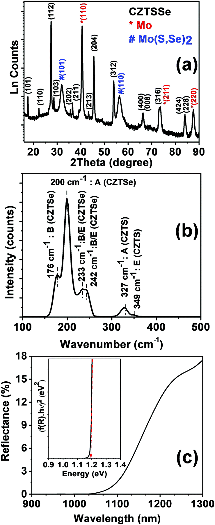 | ||
| Fig. 1 X-ray diffraction pattern (a), Raman spectrum under 514 nm excitation (b) and diffuse reflectance spectrum of as grown CZTSSe films (c). The inset in (c) shows a modified Tauc's plot using the Kubelka–Munk transformation of reflectance, resulting in an optical band gap of 1.18 eV. The structural and optical information are consistent with a I-4 phase with the composition Cu1.6ZnSn0.9(S0.23Se0.77)4. | ||
To ascertain the phase purity of CZTSSe, a Rietveld refinement of the peaks associated with the absorber was performed (ESI,† Fig. S1).16,17 The film crystallizes in the kesterite phase (I-4) with unit cell parameters a = 5.6494 (0.0014) Å and c = 11.2835 (0.003) Å. The overall composition obtained from site occupancies is Cu1.6ZnSn0.9(S0.23Se0.77)4, while other structural parameters, such as atomic positions, are included in the ESI† (Table S1). This Cu-deficient and Zn-rich composition is typical of CZTSSe employed in high-performance solar cells.7 No secondary phases of CZTSSe, e.g. binary metal sulfo-selenide and ternary Cu2Sn(S,Se)3, are identified in the XRD analysis.
Further evidence of the film crystallographic phase is provided by the Raman spectrum shown in Fig. 1b, measured under an excitation at 514 nm. The spectrum shows two distinct regions pertaining to vibrational modes of CZTSe and CZTS. The first region, 150 to 260 cm−1, has two sharp peaks at 176 and 200 cm−1 assigned to the B and A symmetry modes, respectively, of CZTSe in the kesterite phase. Two convoluted weak bands at 233 and 242 cm−1 are also observed, which are linked to B/E symmetry modes. The second region, 300 to 360 cm−1, consists of two peaks at 327 and 349 cm−1 linked to the A and E symmetry modes, respectively, of CZTS. The peaks associated with the CZTSe and CZTS phases are blue and red shifted, respectively, in comparison to the Raman mode of the pure kesterites (for, e.g., the A mode: CZTS 338 cm−1 and CZTSe: 196 cm−1). Furthermore, these results are consistent with literature for the sulfoselenide unit cell with a [Se]/[S] ∼ 3, in agreement with the XRD analysis.18
The diffuse reflectance spectrum in Fig. 1c shows a sharp onset close to 1170 nm, characteristic of a direct band-to-band transition. The Kubelka–Munk function as a function of incident photon energy (inset Fig. 1c) is consistent with a direct band gap transition at 1.18 eV, which is also consistent with the degree of selenization obtained from XRD and Raman data.19
The SEM image in Fig. 2a shows a homogeneous and compact polycrystalline film after annealing, featuring grain sizes from 800 to 1400 nm. The cross-sectional SEM image in Fig. 2b allows us to identify three regions: (i) a 1.3 μm thick top CZTSSe layer, (ii) a 200 nm thick Mo layer at the bottom of stack and (iii) a 750 nm intermediate layer generated by the partial conversion of Mo to Mo(S,Se)2. The elemental dispersive analysis of X-rays (EDAX) linescan in Fig. 2c clearly shows that the Se and S signals extend beyond those of Cu, Zn and Sn, overlapping with the signal, confirming the presence of a Mo(S,Se)2 layer. Se appears more prominent at the boundary between CZTSSe/Mo(S,Se)2, while a slight S excess is observed at the Mo(S,Se)2/Mo junction. This trend suggests that MoS2 is initially generated, given that sulfur is already present in the molecular precursor, while Se has to diffuse through the film during annealing. Within the CZTSSe layer, the ratios of [Zn]/[Sn], [Cu]/([Zn] + [Sn]) and [Se]/[S] are 1.11, 0.82, and 2.8, respectively. The overall EDAX composition is consistent with the values estimated from XRD, Raman and band gap onset.
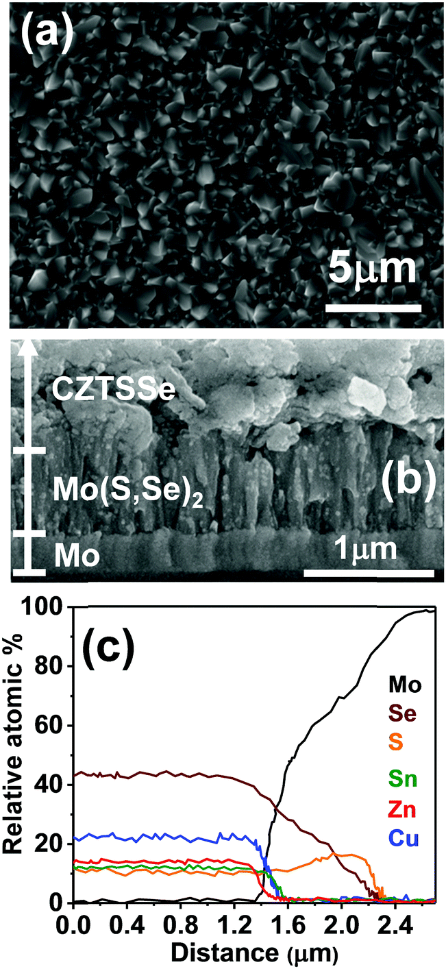 | ||
| Fig. 2 Top (a) and cross-sectional (b) scanning electron micrographs of the annealed CZTSSe film. Composition profile using an EDAX linescan across the CZTSSe/Mo film stack (c). | ||
Current–voltage (J–V) and external quantum efficiency spectra of devices with the structure glass/Mo/CZTSSe/CdS/i-ZnO/Al:ZnO are displayed in Fig. 3, in the absence of top metal contacts or anti-reflecting coating. The total area of the individual cells is 0.25 cm2, defined by mechanically scribing. Fig. 3a illustrates the J–V characteristics of the best cell in the dark and under simulated AM 1.5G illumination, featuring a power conversion efficiency of 5.7%. The open-circuit voltage (VOC), short-circuit current (JSC) and fill factor (FF) estimated for this cell are 396 mV, 27.8 mA cm−2 and 52%, respectively. The mean performance values for 20 devices are summarized in Table S2 (ESI†), showing a maximum deviation of less than 15%.
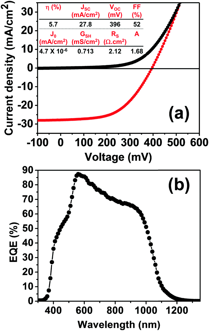 | ||
| Fig. 3 J–V characteristics under 100 mW cm−2 AM 1.5G (a) and external quantum efficiency spectrum (b) of a 0.25 cm2 device with the structure: glass/Mo/CZTSSe/CdS/i-ZnO/Al:ZnO. The reverse saturation current (J0), shunt conductance (GSH), series resistance (RS) and diode factor (A) derived from the J–V under illumination are provided as inset to (a). | ||
Fig. 3b displays the external quantum efficiency (EQE) spectrum, showing a maximum value close to 90% at 2.21 eV. Estimation of the band-gap from the first derivative of the EQE spectrum with respect to photon energy yields a value of 1.17 eV, while a similar value was obtained from the intercept of (hν(−ln(1 − EQE)))2versus hν. This band-gap is consistent with the analysis of the diffuse-reflectance data (Fig. 2c). Integrating the EQE spectrum with respect to AM 1.5G results in a value of 27.6 mA cm−2, consistent with the JSC value in Fig. 3a.
As commonly observed in these systems, the major limiting factor in device performance is linked to the VOC deficiency and the low FF. For comparison, the 12.6% champion cell reported by IBM show VOC and FF values of 466 mV and 69.8%, respectively.8 Interfacial and bulk recombination processes are the source of this limiting effect and the rest of the discussion will focus on the latter.
Carrier recombination mechanisms based on photoluminescence measurements
The photoluminescence (PL) spectra of CZTSSe films measured as functions of excitation power and temperature are shown in Fig. 4a and b.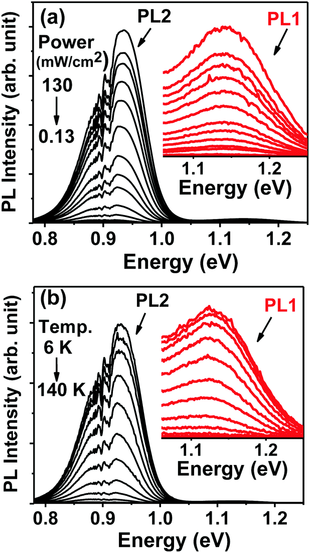 | ||
| Fig. 4 Photoluminescence spectra of CZTSSe films as a function of excitation power (a) and temperature (b). Insets expand on the region associated with PL1. | ||
Two key features are observed, a weak band at 1.14 eV (PL1) and a stronger response at 0.95 eV (PL2). Both bands are found to be asymmetrical in shape, which is characteristic of heavily doped and compensated semiconductors, including kesterites.20–27 As discussed further below, the position of the bands is slightly affected by temperature and power intensity. Signals associated with water absorption around 0.9 eV introduce some interference in the analysis of the PL2 band, becoming a lot more significant at higher temperatures and lower excitation powers.
In order to establish quantitative trends of PL1 and PL2 with respect to excitation intensity and temperature, each of them were fitted to a double sigmoidal function proposed by Krustok et al.,28 which considers asymmetry introduced by phenomena such as band tailing. Fig. 5a shows that the maximum (EPL*) of the PL1 and PL2 bands is shifted to higher energies by approximately 6.5 meV per decade of incident power excitation. In a first approximation, this behavior can be rationalized in terms of the so-called donor–acceptor pair (DAP) recombination mechanism,20
 | (1) |
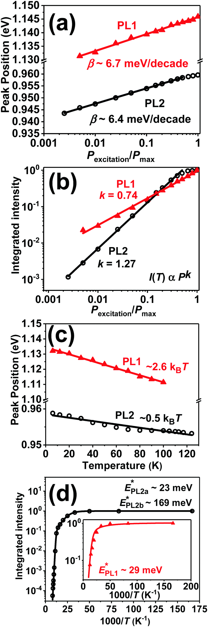 | ||
| Fig. 5 Excitation laser power dependence of the PL peak position (a) and integrated intensity (b). Temperature dependence of the PL peak positions (c) and integrated intensity (d). PL1 is characterized by a single activation energy, while PL2 showed two values depending on the temperature range. | ||
The variation of integrated peak intensity with excitation power is shown in Fig. 5b, revealing a power dependence with exponent values (k) of 1.27 ± 0.02 and 0.74 ± 0.04 for the PL2 and PL1 bands, respectively. The k value of PL1 is consistent with a defect mediated recombination involving localized (trapped) carriers. On the other hand, the behavior of PL2 can be linked to recombination via charge carriers not localized on the defect level, and previous studies have reported k values as large as 1.7 in chalcopyrites and kesterites.21–23 It is also noticeable that the peak position of PL1 has a stronger dependence on temperature than that of PL2, as shown in Fig. 5c. This is further evidence that PL1 involves valence band tail states which effectively become acceptor states at low temperature.23
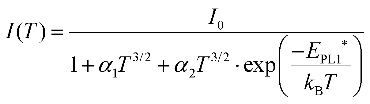
Further valuable information on the nature of PL1 can be gained from the temperature dependence of the peak intensity as shown in Fig. 5d. Thermal PL quenching can be described from a single radiative recombination channel, assuming temperature dependence of the hole capture cross section,28
 | (2) |
 | (3) |
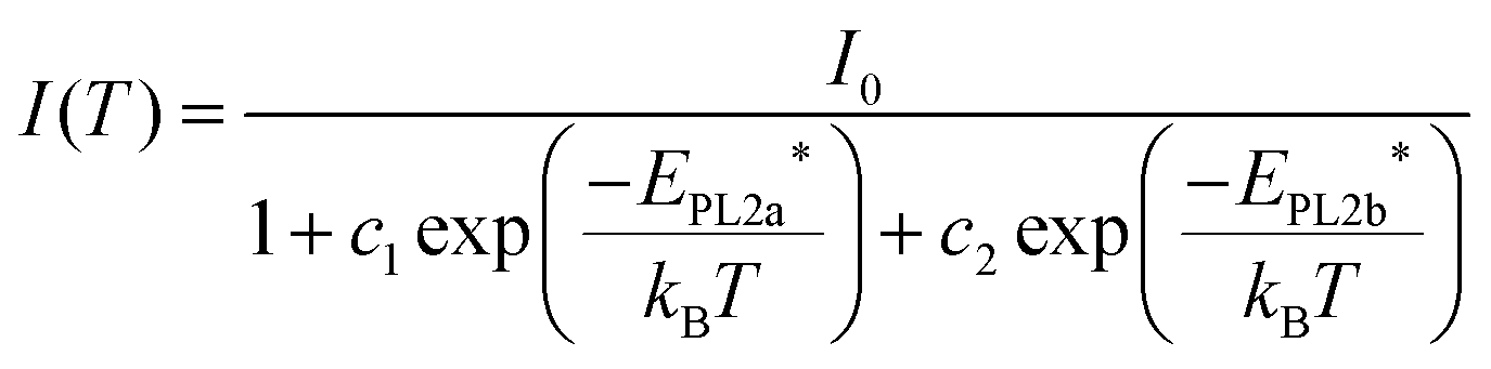
The position and weak temperature dependence of PL2 (Fig. 5c) excludes the possibility of involvement of valence band tail states or DAP recombination (large β value). Thus, the origin of PL2 can be assigned to a transition between the conduction band and a deep acceptor impurity level. The strong dependence of the PL2 peak intensity with temperature (Fig. 5d) is characterized by a complex Arrhenius behavior with two activation energies,25
 | (4) |
Temperature dependence of the device electrical impedance
Impedance spectra of devices recorded up to 1 MHz and between 80 and 340 K are exemplified in Fig. S2a (ESI†). Fig. S2b (ESI†) shows the equivalent circuit used in the impedance analysis, featuring two RC time constants associated with the CZTSSe/CdS (RjCj) and Mo(S,Se)2/CZTSSe (RbCb) junctions, as well as two additional time constants (R1C1 and R2C2) linked to trap states in parallel.15,33–36 The temperature dependences of the various resistance and capacitance elements are illustrated in Fig. S2c–e (ESI†). Fig. S2c (ESI†) shows the decrease of the CZTSSe/CdS junction capacitance (Cj) with decreasing temperature down to a value of 1.55 nF. This geometric limit corresponds to a dielectric thickness of 1.35 μm, which closely agrees with the film thickness measured by SEM. Furthermore, we have performed capacitance–voltage profiling as shown in Fig. S3 (ESI†), following established methodologies.37 The analysis provided a depletion width and doping density at zero bias of 175 nm and 1.6 × 1016 cm−3, respectively.Fig. 6a shows the temperature dependence of the back-contact resistance (Rb), revealing two carrier collection barrier heights of 311 ± 4 meV and 96 ± 1 meV. This complex back contact behavior has been reported in previous studies,34,36 and can be tentatively linked to the CZTSSe/Mo(S,Se)2/Mo double junction. The large barrier heights observed at high temperatures have a strong detrimental effect in device performance, particularly on FF. Recent studies have shown a substantial increase in device performance after mechanically detaching the cell from the Mo film and attaching a fresh back contact.38
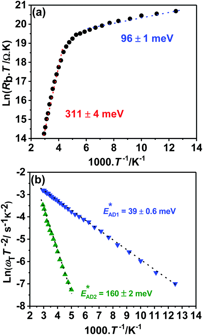 | ||
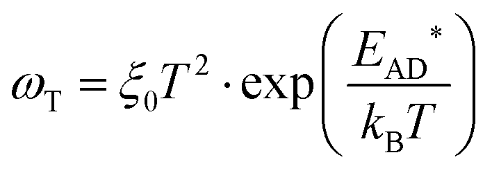
| Fig. 6 Temperature dependence of the back contact, revealing two barrier heights of 311 ± 4 meV and 96 ± 1 meV at high and low temperatures, respectively (a). These back contact barriers heights can be linked to transport across the CZTSSe/Mo(S,Se)2/Mo double-junction. Temperature dependence of the relaxation frequencies of the two acceptor levels (b). The activation energies EAD1* and EAD2* closely correlate with the activation energies of EPL1 and EPL2, respectively. | ||
The temperature dependence of the trap states (ωT = 1/RC) are characterized by an Arrhenius type of behavior as shown in Fig. 6b:15,33–36
 | (5) |
Fig. 7 illustrates the main finding of the combined spectroscopic and impedance studies, highlighting:
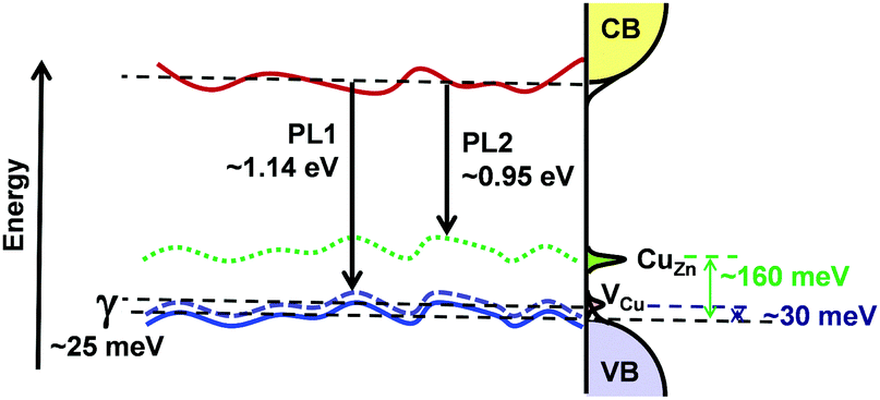 | ||
| Fig. 7 Schematic one dimension illustration of the band gap, showing tail states and the position of carrier capture by the acceptor states at room temperature. | ||
i. Band edges affected by potential fluctuations with an average depth of γ ≈ 25 meV
ii. Shallow acceptor states, assigned to VCu, located 30 meV above the valence band edge with an electron capture time constant (R1C1) of the order of 100 μs
iii. Deeper acceptor states, linked to CuZn antisite clusters, located at 160 meV above the valence band edge with a time constant of 500 μs at room temperature.
VCu is the acceptor state with the lowest formation energy in Cu based chalcogenides, such as CIGS and CZTSSe, resulting in the characteristic p-type conductivity of these materials.9 It should be mentioned that DFT calculations are mainly performed in the dilute regime, i.e. assuming isolated (point) defects. However, the charge compensated nature of these materials suggests a high probability of defect clustering which is responsible for the potential fluctuation of the band edges (tail states). These tail states, as well as deep traps introduced by CuZn antisites, are closely linked to bulk recombination and the loss of VOC. Indeed, Monte-Carlo simulations considering the ensemble of defects have predicted potential fluctuations similar to the one obtained in our analysis.11,39
We recognize that important contributions to the observation of CuZn antisite defects have been made on the basis of order parameters estimated from crystallographic analysis40 and Raman features;41 however, linking these parameters to specific recombination pathways and device efficiency in a quantitative manner remains a formidable challenge. If our key assignments are correct, this is a step forward in this direction. However, in order to establish a complete picture linking recombination kinetics and efficiency losses, additional information, such as time resolved PL measurements, is required as well as techniques capable of probing deeper states in the band gap, such as deep level transient spectroscopy (DLTS).42 Indeed, Sn anti-sites are expected to generate mid-gap states, which may also have a significant contribution to device performance.13,36,43 Finally, charge compensation will arise from defect states located close to the conduction band, most probably connected to ZnCu antisite clusters.12 Establishing spectroscopic and electrical signatures of these parameters is crucial in order to fully comprehend the recombination processes limiting the performance of the devices.
Conclusions
Our studies provide a clear link between spectroscopic and electrical signatures of trap states in CZTSSe films obtained by solution processing of molecular precursors and reactive annealing in the presence of Se. Quantitative XRD, Raman and diffuse reflectance spectroscopy and EDAX reveal highly pure I-4 phase with the stoichiometry Cu1.6ZnSn0.9(S0.23Se0.77)4 and a band gap of 1.18 eV. Devices with the structure Mo/CZTSSe/CdS/i-ZnO/AZO were fabricated with a total area of 0.25 cm2, with no top metal contact or antireflective coating. The best cell performance provided a VOC, JSC and FF of 396 mV, 27.8 mA cm−2 and 52%, respectively, corresponding to a power conversion efficiency of 5.7%. Quantitative analysis of variable temperature PL and impedance spectroscopy allowed us to identify two key acceptor states located at 160 and 30 meV from the valence band edge. The deeper state is characterized by a broad and asymmetric PL band (PL2), featuring two activation barriers as a function of temperature. We rationalize this observation in terms of the emission from tail states in the conduction band (linked to potential fluctuations with an average depth of 23 meV) to an acceptor state assigned to a CuZn antisite. On the other hand, PL1 involves charge localized in an acceptor state assigned to VCu. Impedance spectroscopy of the complete devices exhibited two time-constants associated with states featuring the same activation energy obtained from the PL spectra. This important correlation enables us not only to confirm the acceptor nature of the states, but also provides valuable information with regards to the kinetics of charge trapping. These observations are crucially important for several reasons: (1) a direct link between the bulk spectroscopic features of the absorber layer and the device electrical properties, and (2) correlation between electron trapping and parameters such as the average band edge potential fluctuation, which is related to material disorder.Conflicts of interest
There are no conflicts to declare.Acknowledgements
DT, JWB and DJF are indebted to the Engineering and Physical Sciences Research Council (EPSRC) funded PVTEAM grant (EP/L017792/1). DJF acknowledges Institute of Advanced Studies of the University of Bristol support of a University Research Fellowship 2016. Impedance analysis was performed with a Solartron analyzer procured under EPSRC CDT Capital grant EP/K035746/1. Microscopic imaging and analysis were done at the Chemical Imaging Facility, University of Bristol, with equipment funded by EPSRC Grant “Atoms to Applications” (EP/K035746/1). The authors are grateful for measurement facilities provided at CREST, Loughborough University and the Department of Physics, SUPA, Strathclyde University.Notes and references
- V. Steinmann, R. E. Brandt and T. Buonassisi, Nat. Photonics, 2015, 9, 355–357 CrossRef CAS.
- J.-P. Correa-Baena, A. Abate, M. Saliba, W. Tress, T. Jesper Jacobsson, M. Grätzel and A. Hagfeldt, Energy Environ. Sci., 2017, 10, 710–727 CAS.
- J. S. Manser, M. I. Saidaminov, J. A. Christians, O. M. Bakr and P. V. Kamat, Acc. Chem. Res., 2016, 49, 330–338 CrossRef CAS PubMed.
- E. Tenuta, C. Zheng and O. Rubel, Sci. Rep., 2016, 6, 37654 CrossRef CAS PubMed.
- P. Jackson, R. Wuerz, D. Hariskos, E. Lotter, W. Witte and M. Powalla, Phys. Status Solidi RRL, 2016, 10, 583–586 CrossRef CAS.
- S. K. Wallace, D. B. Mitzi and A. Walsh, ACS Energy Lett., 2017, 2, 776–779 CrossRef CAS.
- X. Liu, Y. Feng, H. Cui, F. Liu, X. Hao, G. Conibeer, D. B. Mitzi and M. Green, Prog. Photovoltaics, 2016, 24, 879–898 Search PubMed.
- J. Kim, H. Hiroi, T. K. Todorov, O. Gunawan, M. Kuwahara, T. Gokmen, D. Nair, M. Hopstaken, B. Shin, Y. S. Lee, W. Wang, H. Sugimoto and D. B. Mitzi, Adv. Mater., 2014, 26, 7427–7431 CrossRef CAS PubMed.
- I. Repins, N. Vora, C. Beall, S.-H. Wei, Y. Yan, M. Romero, G. Teeter, H. Du, B. To, M. Young and R. Noufi, MRS Proc., 2011, 1324, d17 Search PubMed.
- O. Gunawan, T. K. Todorov and D. B. Mitzi, Appl. Phys. Lett., 2010, 97, 233506 CrossRef.
- P. Zawadzki, A. Zakutayev and S. Lany, Phys. Rev. Appl., 2015, 3, 34007 CrossRef.
- S. Chen, A. Walsh, X.-G. Gong and S.-H. Wei, Adv. Mater., 2013, 25, 1522–1539 CrossRef CAS PubMed.
- D. Tiwari, T. Koehler, X. Lin, R. Harniman, I. Griffiths, L. Wang, D. Cherns, R. Klenk and D. J. Fermin, Chem. Mater., 2016, 28, 4991–4997 CrossRef CAS.
- C. M. Fella, Y. E. Romanyuk and A. N. Tiwari, Sol. Energy Mater. Sol. Cells, 2013, 119, 276–277 CrossRef CAS.
- D. Tiwari, T. Koehler, X. Lin, A. Sarua, R. Harniman, L. Wang, R. Klenk and D. J. Fermin, ACS Appl. Mater. Interfaces, 2017, 9, 2301–2308 CAS.
- J. Rodríguez-Carvajal, Phys. B, 1993, 192, 55–69 CrossRef.
- D. M. Berg, M. Arasimowicz, R. Djemour, L. Gutay, S. Siebentritt, S. Schorr, X. Fontane, V. Izquierdo-Roca, A. Perez-Rodriguez and P. J. Dale, Thin Solid Films, 2014, 569, 113–123 CrossRef CAS.
- M. Dimitrievska, H. Xie, A. Fairbrother, X. Fontané, G. Gurieva, E. Saucedo, A. Pérez-Rodríguez, S. Schorr and V. Izquierdo-Roca, Appl. Phys. Lett., 2014, 105, 31913 CrossRef.
- W. Sun, X. Geng, J. C. Armstrong, J. Cui and T. Chen, 2014 IEEE 40th Photovolt. Spec. Conf., 2014, pp. 0421–0424.
- A. P. Levanyuk and V. V. Osipov, Sov. Phys. Uspekhi, 1981, 24, 187–215 CrossRef.
- J. P. Teixeira, R. A. Sousa, M. G. Sousa, A. F. Da Cunha, P. A. Fernandes, P. M. P. Salome and J. P. Leitao, Phys. Rev. B: Condens. Matter Mater. Phys., 2014, 90, 235202 CrossRef.
- J. Krustok, R. Josepson, M. Danilson and D. Meissner, Sol. Energy, 2010, 84, 379–383 CrossRef CAS.
- J. Márquez-Prieto, M. V. Yakushev, I. Forbes, J. Krustok, P. R. Edwards, V. D. Zhivulko, O. M. Borodavchenko, A. V. Mudryi, M. Dimitrievska, V. Izquerdo-Roca, N. M. Pearsall and R. W. Martin, Sol. Energy Mater. Sol. Cells, 2016, 152, 42–50 CrossRef.
- E. Kask, M. Grossberg, R. Josepson, P. Salu, K. Timmo and J. Krustok, Mater. Sci. Semicond. Process., 2013, 16, 992–996 CrossRef CAS.
- S. Levcenko, J. Just, A. Redinger, G. Larramona, S. Bourdais, G. Dennler, A. Jacob and T. Unold, Phys. Rev. Appl., 2016, 5, 24004 CrossRef.
- M. Grossberg, J. Krustok, K. Timmo and M. Altosaar, Thin Solid Films, 2009, 517, 2489–2492 CrossRef CAS.
- M. Grossberg, J. Krustok, J. Raudoja, K. Timmo, M. Altosaar and T. Raadik, Thin Solid Films, 2011, 519, 7403–7406 CrossRef CAS.
- J. Krustok, H. Collan, M. Yakushev and K. Hjelt, Phys. Scr., 1999, T79, 179–182 CrossRef CAS.
- E. Zacks and A. Halperin, Phys. Rev. B: Solid State, 1972, 6, 3072–3075 CrossRef CAS.
- S. Schorr, Sol. Energy Mater. Sol. Cells, 2011, 95, 1482–1488 CrossRef CAS.
- S. Chen, L. W. Wang, A. Walsh, X. G. Gong and S. H. Wei, Appl. Phys. Lett., 2012, 101, 223901 CrossRef.
- S. Chen, X. G. Gong, A. Walsh and S. H. Wei, Appl. Phys. Lett., 2010, 96, 21902 CrossRef.
- T. Walter, R. Herberholz, C. Müller and H. W. Schock, J. Appl. Phys., 1996, 80, 4411–4420 CrossRef CAS.
- P. A. Fernandes, A. F. Sartori, P. M. P. Salome, J. Malaquias, A. F. Da Cunha, M. P. F. Gracia and J. C. Gonzalez, Appl. Phys. Lett., 2012, 100, 233504 CrossRef.
- Y. Y. Proskuryakov, K. Durose, B. M. Taele and S. Oelting, J. Appl. Phys., 2007, 102, 24504 CrossRef.
- D. Tiwari, T. Koehler, R. Klenk and D. J. Fermin, Sustainable Energy Fuels, 2017, 1, 899–906 CAS.
- J. T. Heath, J. D. Cohen and W. N. Shafarman, J. Appl. Phys., 2004, 95, 1000–1010 CrossRef CAS.
- K. Sardashti, E. Chagarov, P. D. Antunez, T. S. Gershon, S. T. Ueda, T. Gokmen, D. Bishop, R. Haight and A. C. Kummel, ACS Appl. Mater. Interfaces, 2017, 9, 17024–17033 CAS.
- K. Yu and E. A. Carter, Chem. Mater., 2016, 28, 864–869 CrossRef CAS.
- D. M. Tobbens, G. Gurieva, S. Levcenko, T. Unold and S. Schorr, Phys. Status Solidi B, 2016, 253, 1890–1897 CrossRef.
- J. J. S. Scragg, J. K. Larsen, M. Kumar, C. Persson, J. Sendler, S. Siebentritt and C. Platzer Björkman, Phys. Status Solidi B, 2016, 253, 247–254 CrossRef CAS.
- J. V. Li, D. Kuciauskas, M. R. Young and I. L. Repins, Appl. Phys. Lett., 2013, 102, 163905 CrossRef.
- N. A. Kattan, I. J. Griffiths, D. Cherns and D. J. Fermín, Nanoscale, 2016, 8, 14369–14373 RSC.
Footnotes |
| † Electronic supplementary information (ESI) available: This includes figures and tables showing Rietveld refinement on selective X-ray diffraction from CZTSSe, structural parameters, statistics of solar cell parameters, characteristic impedance spectrum and fitting, equivalent circuit, temperature dependence of electrical parameters, and the capacitance–voltage profile of a solar cell. See DOI: 10.1039/c7tc03953k |
| ‡ Data are available at the University of Bristol data repository, data.bris, at https://doi.org/10.5523/bris.crb6e8flbup12pguihul9xye2 |
| § Further details of the crystal structure investigation(s) may be obtained from the Fachinformationszentrum Karlsruhe, 76344 Eggenstein-Leopoldshafen (Germany), on quoting the depository number CSD-433445. |
| This journal is © The Royal Society of Chemistry 2017 |