
 Open Access Article
 This Open Access Article is licensed under a
 Creative Commons Attribution 3.0 Unported Licence
Valence band modification of Cr2O3 by Ni-doping: creating a high figure of merit p-type TCO†
Elisabetta
Arca‡
 *a,
Aoife B.
Kehoe
b,
Tim D.
Veal
c,
Aleksey
Shmeliov
b,
David O.
Scanlon
de,
Clive
Downing
b,
Dermot
Daly
b,
Daragh
Mullarkey
a,
Igor V.
Shvets
a,
Valeria
Nicolosi
b and
Graeme W.
Watson
b
*a,
Aoife B.
Kehoe
b,
Tim D.
Veal
c,
Aleksey
Shmeliov
b,
David O.
Scanlon
de,
Clive
Downing
b,
Dermot
Daly
b,
Daragh
Mullarkey
a,
Igor V.
Shvets
a,
Valeria
Nicolosi
b and
Graeme W.
Watson
b
aSchool of Physics and CRANN, Trinity College Dublin, Dublin, Ireland. E-mail: earca@tcd.ie
bSchool of Chemistry and CRANN, Trinity College Dublin, Dublin, Ireland
cStephenson Institute for Renewable Energy and Department of Physics, School of Physical Sciences, University of Liverpool, Liverpool, L69 7ZF, UK
dUniversity College London, Kathleen Lonsdale Materials Chemistry, Department of Chemistry, 20 Gordon Street, London WC1H 0AJ, UK
eDiamond Light Source Ltd., Diamond House, Harwell Science and Innovation Campus, Didcot, Oxfordshire OX11 0DE, UK
First published on 28th November 2017
Abstract
p-Type transparent conductors and semiconductors still suffer from remarkably low performance compared to their more widespread n-type counterparts, despite extensive investigation into their development. In this contribution, we present a comparative study on the defect chemistry of potential p-type transparent conducting oxides Mg-doped and Ni-doped Cr2O3. Conductivities as high as 28 S cm−1 were achieved by Ni-doping. By benchmarking crystallography and spectroscopy characterization against density functional theory calculations, we show that the incorporation of Ni into Cr2O3 contributes to the composition of the valence band, making the formed holes more delocalized, while Mg states do not interact with the valence band in Mg-doped Cr2O3. Furthermore, it is experimentally proven that Ni has a higher solubility in Cr2O3 than Mg, at least in the highly non-thermodynamic deposition conditions used for these experiments, which directly translates into a higher acceptor concentration. The combination of these two effects means that Ni is a more effective acceptor in Cr2O3 than Mg and explains the improved conductivity observed for the former.
1 Introduction
Transparent conducting oxides (TCOs) are a particular class of materials which combine both optical transparency and electrical conductivity.1–4 This peculiarity arises from the stringent dual requirements of having the first allowed optical transition at energy values higher than 3.1 eV and having uncompensated shallow donor (or acceptor) states close to the bottom (top) of the conduction band minimum (valence band maximum).1–4 The transparency window in the visible range is normally realized by (i) having a material with a wide fundamental band gap, such as in the case of n-type BaSnO35 or p-type CuAlO2,6 or (ii) having a smaller band gap associated with a forbidden optical transition and the first allowed optical transition higher than 3.1 eV, like in the case of n-type In2O37 or p-type SnO.8 Dopability, either n- or p-type, is achieved via alignment of the band edges of the oxides with respect to the vacuum level and, at the same time, the ability to insert uncompensated defects.9–11To date, p-type transparent conductors and semiconductors have displayed severely poorer properties than their n-type counterparts. So far the best reported p-type TCOs have conductivities in the range of 102 S cm−1, for example delafossite CuCrO2:Mg (conductivity 220 S cm−1 with 30% transparency)12 and layered cobaltate Bi2Sr2Co2Oy (conductivity 222 S cm−1 with 50% transparency).13 More recently, Zhang et al.14 have reported Sr-doped LaCrO3 as a promising new p-type transparent conducting oxide, with LaSr0.25Cr0.75O3 and LaSr0.5Cr0.5O3 achieving conductivities of 15 S cm−1 and 54 S cm−1, respectively, although it was noted that higher conductivities via increased dopant concentration can come at the expense of reduced transparency (54.2% and 42.3%, respectively). These values of conductivity are still two or three orders of magnitude lower than those achieved in n-type TCOs, such as ZnO:Al, In2O3:Sn or SnO2:F, which are in the range of 104 S cm−1.
The major shortcoming of p-type TCOs lies in their poor hole mobility. Despite the fact that high doping levels can be achieved,15 the values of conductivity are inherently hindered by heavy effective masses16,17 or by the highly localized nature of p and d states forming the valence band maximum (VBM), with the latter leading to polaronic conductivities.18–21 Only a few p-type TCOs have shown mobilities reproducibly higher than 1 cm2 V−1 s−1, an example of which is SnO.8,22,23
Overcoming these limitations has stimulated intense research activity in the field, from both an experimental and a theoretical point of view. CuAlO2, the first reported p-type TCO,24 overcomes the limitations of hole localisation on O ions by combining semiconductor Cu2O with transparent insulator Al2O3 such that the Cu d states mix with the O p states in the valence band, promoting delocalization. Various materials were considered over the past two decades include delafossite structures,21,25–31 oxychalcogenides,32–35 spinel structures,36–39 cobaltates,13 more complex or exotic structures such as KAg11(VO4)440 and recently, Ha et al. have expanded the concept of Sn(II)-based oxide as suitable materials to achieve low effective mass p-type TCOs.41
Recently, we demonstrated the possibility of Cr2O3 as p-type transparent semiconductor oxide, by doping it with Mg to improve its electrical conductivity and retain the transparency properties by introducing an ammonium precursor in the solution.42,43 Lately, Cr2O3 has received considerable attention as a p-type transparent conductor,43–47 with a few reports also discussing the possibility of n-type behavior in Cr2O3 by doping it with Ti.48–51 While Mg is a popular choice in the literature as a hole dopant for Cr2O3,46,52,53 further improvement can be achieved if shallower acceptors than Mg are used. To this end, Ni has been considered,53,54 with the highest conductivity of 5 S cm−1 recently achieved by Arca et al.45
In this contribution, we compare the effect of p-type dopants Mg and Ni in epitaxial Cr2O3 films. We show that Ni is a far more effective dopant than Mg, achieving conductivities an order of magnitude higher. Moreover, through a combination of crystallography, spectroscopy and density functional theory (DFT) calculations, we attempt to establish the origin of the improved conductivities and in particular the role of Ni as a more effective acceptor than Mg.
2 Experimental details
Cr2O3 films were deposited on a single side polished sapphire (c-Al2O3, (0001)-oriented) mono crystalline substrate using a pulsed laser deposition chamber (SURFACE) operating at a base pressure of 5 × 10⁻⁷ bar. A KrF laser (λ = 248 nm) was used at a repetition rate of 10 Hz. The laser density on the target was adjusted to be 0.8 J cm−2. Ni-Doped, Mg-doped and an undoped target were prepared by solid state reaction. Details of the target preparation are reported elsewhere.45,46 For the deposition, different combinations of temperature and pressure were tested. Highest conductivity, while still preserving phase purity, were found using deposition temperature of 773 °C and 923 °C for Ni-doping and Mg-doping, respectively, and optimum deposition pressure of 1 × 10⁻⁴ bar for both dopants. For both target and thin films, the composition is expressed based on the cation ratio, i.e. the ratio Mat/(Mat + Crat) where M is either Mg or Ni. After each deposition, films were subjected to structural characterization to verify the purity of the phase deposited. To this end, High Resolution X-ray Diffraction (HRXRD) was performed using a Bruker D8 Discover. The thickness of each individual sample was determined by X-Ray Reflectivity (XRR). The effect of doping on the electronic properties of the films was determined by X-ray Photoelectron Spectroscopy (XPS) using an Omicron Multi-Probe XPS equipped with a monochromated Al Kα X-ray source in conjunction with an Omicron EA 125 hemispherical analyser. A pass energy of 20 eV was used, which combined with detector and source resolutions, brings the resolution up to 0.5 eV. For undoped, insulating samples, an Omicron CN 10 charge neutralizer was used during XPS acquisition. Beam energy, emission current, and deflection were optimized to achieve a Full Width at Half Maximum (FWHM) of the O 1s peak comparable to the line-width typical of samples not affected by charging (FWHM = 1.2 eV). Samples were loaded into the XPS chamber immediately after deposition to minimize contamination by exposure to atmospheric gases. We realigned all the spectra so that the signal of the aliphatic C 1s core-level meets the standard value of 285 eV. The realignment was only of about 0.2 eV for all conductive samples, and for some of them, it was not even necessary as the signal of adventitious C was already coincident with a binding energy of 285 eV. Electrical characterization was performed in a 4 point probe apparatus using a linear configuration and computer controlled Keithley 2400 source meter. Conductivity values were calculated based on the sheet resistance and thickness measurements as determined by XRR. Additional microstructural and compositional characterization was performed by Transmission Electron Microscopy (TEM). Lamellae were prepared using a gallium based Focused Ion Beam system (Carl Zeiss Auriga 40). A lamella was milled in the region of interest and was then placed on a TEM grid using the in situ lift out technique. The lifted out lamella was subsequently thinned to ∼150 nm with a 15 kV at 200 pA ion beam and then polished to ∼50 nm in the region of interest with a 5 kV at 20 pA ion beam. High-resolution TEM (HRTEM) images were acquired using a FEI Titan operated at 300 keV. Atomically resolved annular dark-field (ADF) scanning TEM (STEM) images were obtained using Nion UltraSTEM operated at 200 keV with collection angles of 99–200 mrad. Energy dispersive X-ray (EDX) maps were acquired using a Bruker 100 mm2 windowless EDX available in the Nion UltraSTEM.3 Computational details
All DFT calculations were carried out using the VASP package,55–57 which models crystalline systems by using periodic boundary conditions and expanding crystal wave functions in terms of a plane wave basis set. Interactions between the core states (represented by atomic functions) and valence electrons (described by plane waves) are modelled using the projector augmented wave (PAW) method, with the cores defined here as Cr:[Ar], O:[He], Mg:[Be], and Ni:[Mg]. The PBE functional was used to describe exchange and correlation,58 with +U values59 to combat self-interaction error applied to the Cr 3d states, due to the highly localized nature of d states, and to the O 2p states, due to the importance of accurately modelling the typically O 2p dominated valence band of p-type oxides. U values of 3 eV and 5 eV, respectively, were derived from comparison to XPS spectra to best reproduce valence band shape and features as outlined in our previous study on Mg-doped Cr2O3.46 A U of 5.3 eV was also applied to the Ni d states, a value which has been widely used in the literature to model Ni oxide systems with PBE.60,61 A k-point mesh of Γ-centred 2 × 2 × 1, a plane wave cut-off of 400 eV, and a force convergence criterion of 0.01 eV Å−1 were used to model the 120 atom 2 × 2 × 1 expansion of the 30 atom hexagonal unit cell. The formation energy (Ef(D,q)) of a defect (D) in each of its possible charge states (q) was calculated according to eqn (1). | (1) |
The first term, ED,q − EP, is the difference in energy between the defective and pure systems. In the second term, ni is the number of atoms of type i taken from or added to an external reservoir, as a function of both the elemental reference energies calculated from their standard states (Ei) and chemical potentials to represent the equilibrium growth conditions (μi). The chemical potentials are found with reference to the PBE + U calculated formation energy of pure Cr2O3, −12.54 eV. The formation energies of CrO and CrO2 were also calculated to determine if they are competing phases under O-poor or O-rich conditions, respectively, but this was found not to be the case. The O-rich chemical potential limits were thus calculated to be μCr = −6.27 eV and μO = 0 eV, and the O-poor limits are μCr = 0 eV and μO = −4.18 eV. For the doped systems, μMg and μNi were calculated using the formation energies of their parent oxides MgO and NiO, resulting in μMg = 3.53 eV and μNi = −2.94 eV under O-rich conditions and μMg = 0 eV and μNi = 0 eV in the O-poor regime.
The third term in eqn (1) includes the charge state of the defect and is dependent on the electron chemical potential (EFermi) and the VBM eigenvalue of the pure system. Finally, Ealign aligns the electrostatic potential between the pure and defective systems and corrects for finite-size effects in charged defect calculations,62 with a value of 12.6 used for the dielectric constant based on the average of the experimentally reported values of 13.0 parallel to the a axis and 11.8 parallel to the c axis.63 The thermodynamic transition levels of each defect are also calculated as in eqn (2), defined as the Fermi level at which different charge states q and q′ of a particular defect have the same formation energy.
 | (2) |
4 Results
A target with a Ni cationic content of 7 at% was prepared, with phase pure films achieved at a deposition temperature of 773 K. This temperature was chosen as spurious peaks were present in the XRD pattern at any other deposition temperature tested (823 K, 873 K and 923 K), as shown in Fig. 1. These peaks, resulting from the formation of competing phases such as NiCrO4 and NiO, were not observed at any value of temperature tested over the range 773 K to 873 K in our previous investigation using 5 at% Ni-doped targets.45 All data on Mg-doped Cr2O3 presented herein is based on a target with a Cr![[thin space (1/6-em)]](https://www.rsc.org/images/entities/char_2009.gif) :Mg ratio of 94:6, the concentration with which the best conductivities were achieved in our previous work.46 These concentrations were found to be those at which no spurious phase were formed, and thus were taken to be the highest value of dopant that, experimentally, could be inserted in the material. The lack of spurious phase as determined by the XRD or TEM analysis was determined to be the solubility limit for both dopants.
:Mg ratio of 94:6, the concentration with which the best conductivities were achieved in our previous work.46 These concentrations were found to be those at which no spurious phase were formed, and thus were taken to be the highest value of dopant that, experimentally, could be inserted in the material. The lack of spurious phase as determined by the XRD or TEM analysis was determined to be the solubility limit for both dopants.
 | ||
| Fig. 1 XRD pattern of Ni-doped films grown out of the 7 at% target at 773 K (black) and 923 K (red). Samples grown at 823 K and 873 K show a very similar pattern to that recorded for the films deposited at 923 K. | ||
HRXRD patterns of both Ni-doped and Mg-doped Cr2O3 are reported in Fig. 2. Rocking curve measurements around the main Cr2O3 (006) reflection were performed to assess the defect density in both films. As shown in the inset in Fig. 2, the line-shape can be reconstructed by using two Gaussian components. Similar to previous literature reports,64,65 the broader component is attributed to a higher density of defects in the interface region between the substrate and the heteroepitaxial films, whereas the second sharper component is relative to the over-layer, whose density of defects is notably reduced. This is common to both the Mg- and Ni-doped films, and the relative full width at half maximum (FWHM) are comparable: the sharper and broader components for Mg-doped films have FWHM of 86arcsec and 972arcsec, respectively, while the same components for Ni-doped films have values of 93arcsec and 540arcsec, respectively. The values of FWHM of the sharpest component are thus comparable, which means that the density of structural defects is similar.
 | ||
| Fig. 2 HRXRD of Ni-doped and Mg-doped Cr2O3 films. | ||
A decrease in the value of the c parameter is observed in both the case of Ni- (13.596 Å) and Mg-doping (13.614 Å) relative to the undoped films (13.650 Å). This shift may appear counterintuitive: while ionic radii can vary substantially depending on the coordination number, for a substitutional type of impurity and a coordination number of 6, both Mg(II) (86 pm) and Ni(II) (83 pm) are expected to have a higher ionic radius than Cr(III) (75.5 pm).66 This contraction of the crystallographic cell despite inserting ions of a higher ionic radii has been previously observed in the literature, for example for Cu2−2xZnxO.67 The quality of both Ni- and Mg-doped samples was further analyzed by HRTEM and atomically resolved ADF STEM to assess if nanoclusters of spurious phases were present. The total area examined for Ni- and Mg doped-lamellae is approximately 700 nm × 70 nm and 700 nm × 40 nm, respectively. Two large area images are shown in the Supplementary information 1 and 2 (ESI†). Additionally, the crystal structure of Cr2O3 and two representative images of Ni-doped Cr2O3 obtained from ADF STEM are shown in Fig. 3. No spurious phases have been detected, and only rare defective regions where interstitial atoms are clearly visible, have been observed for Ni doped films (Fig. 3(c)). Similar results were observed for the Mg-doped sample, albeit without interstitial defects, as shown in the Fig. S3 (ESI†). HRTEM images (Supplementary information 4 and 5, ESI†) confirmed the absence of spurious phases. Notably, forbidden reflections are present in the Fast Fourier Transforms (FFT) of the HRTEM images. Their presence can be attributed to both dynamical scattering effects and the substitution of Ni or Mg on a Cr site. These results further support the conclusions drawn according the XRD analysis, confirming the absence of spurious phases even below the detection limit of the high resolution diffractometer used for this study.
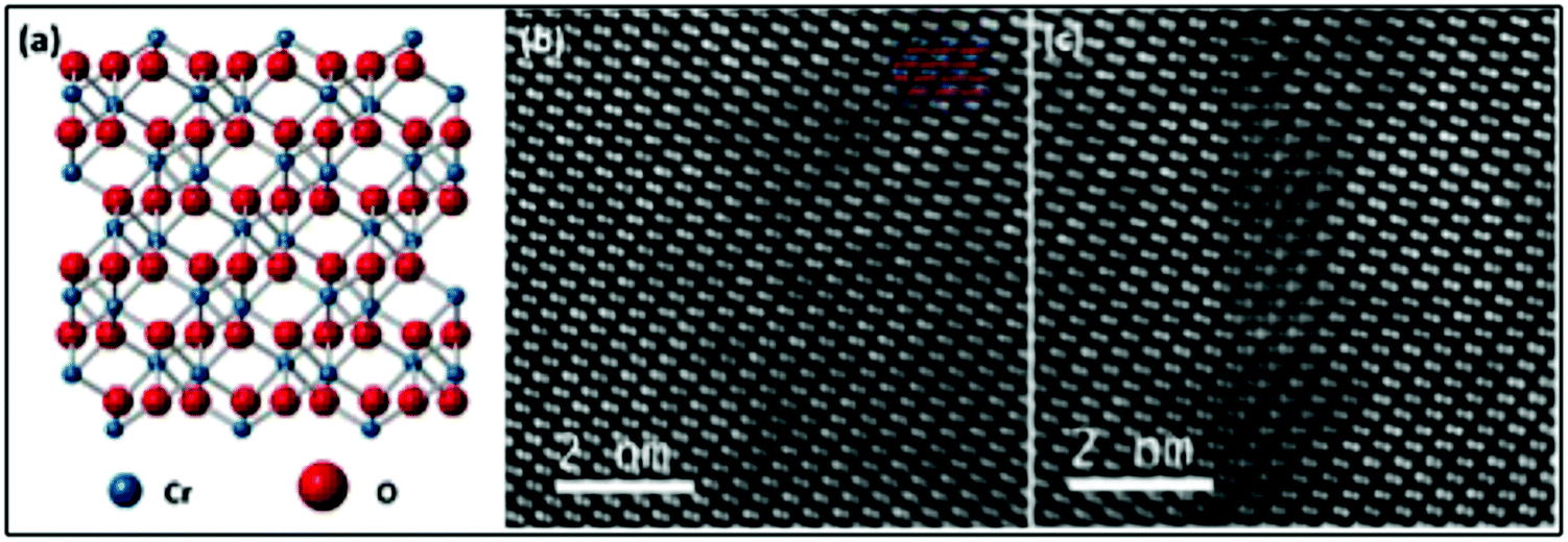 | ||
| Fig. 3 (a) Structure of Cr2O3 along [100] direction, with Cr and O atoms shown in blue and red, respectively. (b) and (c) ADF STEM images of Ni doped Cr2O3 lamella showing respectively a region without any crystallographic defect and a region with interstitial atoms. Only Cr columns are visible in the images due to the strong Z-contrast. | ||
The EDX mapping of the Ni and Mg distribution over a wide region, along with the corresponding ADF STEM images, is shown in Fig. 4. As can be seen, Ni and Mg atoms are not homogeneously distributed, and there are regions where the dopant tends to accumulate (such as Region 1 and 2 in respectively subfigure (c) and (d) of Fig. 4) and regions that are poorer in Ni and Mg content (Region 2 and 1 in each subfigure of Fig. 4). Ni concentration in these two regions was found by EDX to be 16 at% and 11 at%, respectively. Mg concentration in Regions 1 and 2 was found to be 6.6 at% and 4.9 at%, respectively. DFT calculations for a 12.5 at% Ni-doped and a 8.3 at% Mg-doped system were performed, in which it was found that it is energetically preferential to place all of the dopants adjacent to one another in clusters instead of being homogeneously distributed throughout the supercell, corroborating the inhomogeneous distributions of Ni and Mg experimentally found throughout the films. Notably, the EDX determined concentration of incorporated Mg is considerably lower than that of Ni despite their similar target compositions. Conductivity measurements were carried out on a large number of films prepared from the 7 at% Ni target. Most samples were measured to have conductivities of around 20 S cm−1, with the best samples reaching 28 S cm−1. This is in comparison to the 5 ± 1 S cm−1 previously measured for samples produced from a 5% Ni-doped target45 and the 1 ± 0.1 S cm−1 obtained from the 6 at% Mg target, the highest conductivity achieved for Mg-doped films over a range of tested Mg concentrations in our previous work.46
 | ||
| Fig. 4 ADF STEM images of (a) Ni-doped and (b) Mg-doped Cr2O3 with corresponding EDX maps in (c) and (d), respectively, showing the variation in the Ni and Mg concentration across the sample. Regions marked 1 and 2 show areas of increased and decreased dopant concentration, respectively. Pt deposited on the surface of Cr2O3 during lamellae preparation can be seen at the bottom of the images. | ||
This therefore shows both that the higher Ni-doping concentration is conducive to better conductivity and that Ni-doping of Cr2O3 results in an improvement in electronic conductivity of more than an order of magnitude over Mg-doping. Notably, the conductivity of samples prepared with the 7 at% Ni target decreases significantly with increasing deposition temperature as competing phases are formed, as seen from Fig. 5 (top panel). The improvement in conductivity of Ni-doping versus Mg-doping is directly correlated to the lower activation energy observed for Ni-doping (70 meV as determined from the Arrhenius plot shown in Fig. 5 (bottom panel)) in comparison to the Mg-doping (170 meV). While the XRD pattern of the Ni doped samples having 20 S cm−1 shown in Fig. 1 are symmetric, the sample having 28 S cm−1 show a non-perfectly symmetric peak. Variations in Ni concentrations together with small defective regions, as identified by TEM and EDX, are most likely the cause for the asymmetry in the XRD peak associated with this highly conductive sample, yet their presence seems to be non-deleterious for the electrical properties, as noted by the high conductivities of the films.
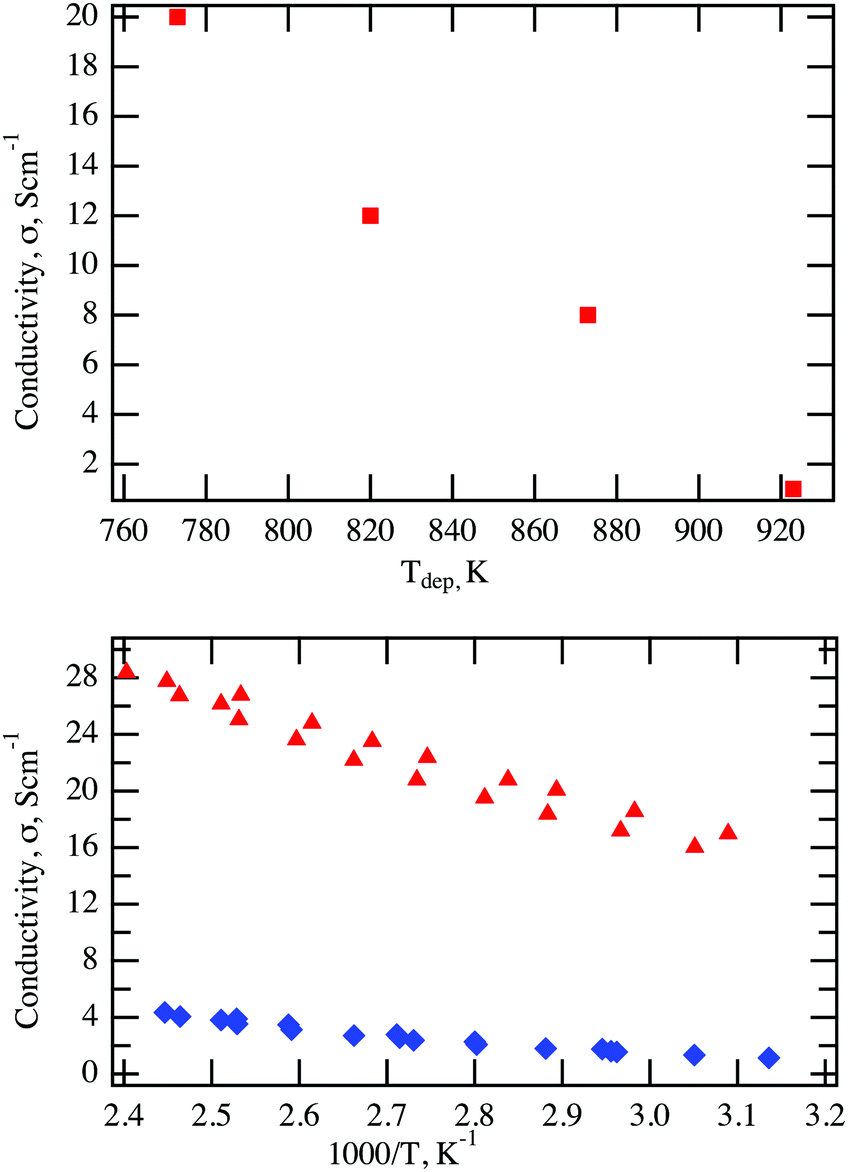 | ||
| Fig. 5 (top panel) The conductivity of Ni-doped Cr2O3 prepared with a 7% Ni target as a function of deposition temperature and (bottom panel) comparison between the Arrhenius plot of a Ni-doped (red triangles) and a Mg-doped (blue diamonds) Cr2O3 thin films. | ||
The optical properties of the Ni-doped films having conductivity equal or higher than 20 S cm−1 are shown in Fig. 6. Transmittance for Ni-doped films ranges from 55% to 35% across the visible range, with an average value of 40%. These values are comparable to those previously reported for Mg-doped samples46 (from 52% to 40% across the visible spectra). A major limitation to transmittance is the reflectance loss due to the large difference between the refractive index of both air and sapphire in comparison to Cr2O3, which is equal or higher than 20% across the entire spectral range.
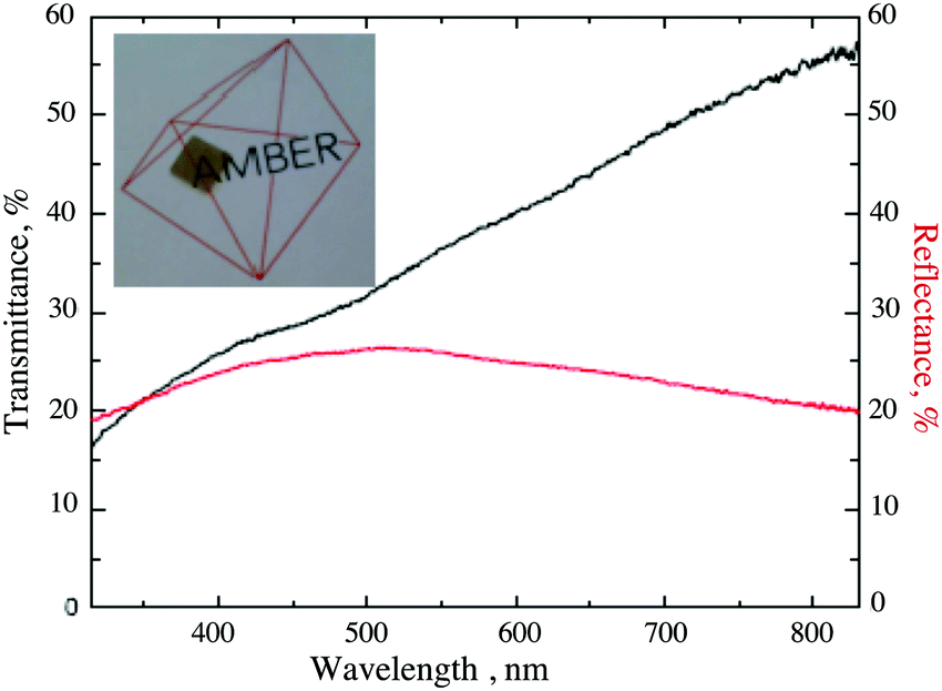 | ||
| Fig. 6 Visible transmittance (black line) and reflectance (red line) of a Ni-doped sample. | ||
Using DFT, the transition levels of a Mg ion on a Cr site, a Mg interstitial ion, a Ni ion on a Cr site, and a Ni interstitial ion were calculated, as shown in Fig. 7. Multiple interstitial positions were tested, but the only location in which the dopant relaxed was the “vacant” cation site in the corundum structure, in which one third of the octahedral sites on the cation sublattice are unfilled. Defect formation energies were calculated under both O-rich/Cr-poor and O-poor/Cr-rich conditions using chemical potential limits as outlined above. The intrinsic defects with the lowest formation energy (O peroxide species in the O-rich regime and O vacancy in the O-poor) and the most shallow ionisation level (Cr vacancy and Cr interstitial for O-rich and O-poor conditions, respectively), as calculated in our previous work,46 are shown for comparison.
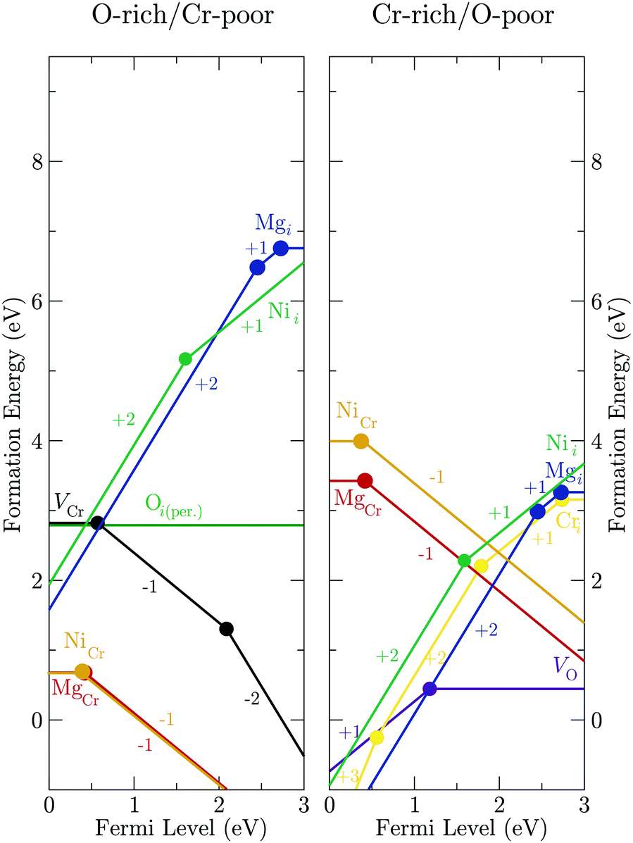 | ||
| Fig. 7 Transition levels diagrams of Mg and Ni interstitial and substitutional ions in Cr2O3, under both O-rich and O-poor conditions. | ||
In the O-rich regime, the Mg ion on a Cr site has a neutral state formation energy of 0.66 eV and a relatively shallow (for a p-type defect) 0/−1 transition level of 0.42 eV. The Ni substitutional ion has a formation energy and first ionisation level of 0.67 eV and 0.40 eV, respectively. Notably, these values are very similar for both dopants. The n-type Mg interstitial and Ni interstitial have formation energies of 6.78 eV and 6.53 eV, respectively, far higher than the p-type substitution defects. The Mg and Ni dopant ions are therefore uncompensated across the span of the band gap, resulting in the experimentally observed p-type conductivity under O-rich conditions.
Under O-poor conditions, where n-type defects should be more favorable, the n-type Mg interstitial has a formation energy and a first ionisation level of 3.25 eV and 0.23 eV, respectively. Mg on a Cr site has a formation energy of 3.42 eV and a first ionisation level of 0.42 eV. An interesting effect of Mg-doping under O-poor conditions is that these two Mg related defects in Cr2O3 intersect on the transition level diagram, which would result in the Fermi level being trapped at 1.92 eV. Therefore, neither n- or p-type conductivity would be expected to be observed when the material is grown in an O-poor environment. A similar situation is observed for Ni-doped Cr2O3 under O poor conditions. Ni on a Cr site has a formation energy of 4.00 eV and a first ionisation level of 0.40 eV. The Ni interstitial has its first transition in the conduction band (1.00 eV above the conduction band minimum), which would be advantageous for n-type conductivity were it not for the fact that the formation energy is prohibitively high at 4.59 eV. As with the Mg-doped system under O-poor conditions, the Fermi level is pinned mid-gap, in this case between the Ni on a Cr site and the Cr interstitial, at an energy of 1.99 eV. As such, for both Mg- and Ni-doping of Cr2O3, electronic conductivity is unlikely to occur when the materials are deposited under O-poor conditions, and only p-type conductivity should be observed in an O-rich regime.
The effect of Ni-doping on the electronic properties of Cr2O3 was assessed by XPS. As XPS is a surface sensitive technique, the stoichiometry of the surface needs to be determined in order to assess if the XPS determined density of states are a good representation of the material's bulk properties. The Ni concentration at the surface was determined by deconvolution of the Cr 3s and Ni 3p peaks as shown in Fig. 8 for the films grown using 5 at% and 7 at% doped targets. These were then compared to the bulk values as determined by EDX spectroscopy. The Cr 3s and Ni 3p photoelectrons were chosen as they have similar binding energies and approximately the same inelastic mean free path (IMFP) of λ = ∼3 nm. Details on how to calculate the IMFP are reported in the ESI.† According to the Beer–Lambert law, 95% of the XPS signal is from 3λ = 9 nm. Curve fitting Cr 3s and Ni 3p regions is complicated by the presence of satellite features associated with the well-known shake-up satellite peaks at higher binding energy than the main peaks. These features are consistent with previous reports for Cr2O3 and NiO and have been fitted in order to be included in determining the total Cr 3s and Ni 3p peak areas and applying the relative sensitivity factors for composition determination.
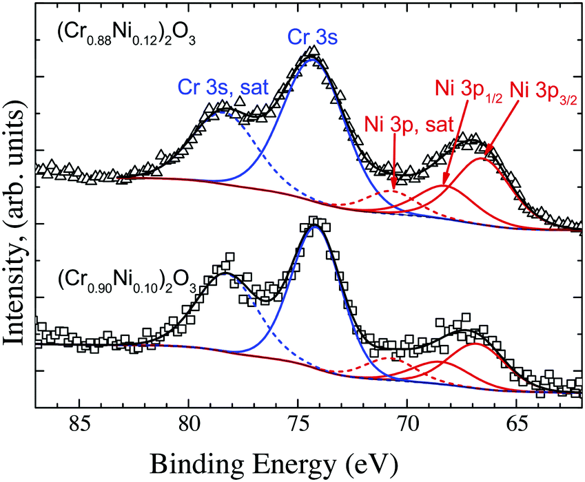 | ||
| Fig. 8 Deconvolution of the Cr 3s and Ni 3p peaks to determine the concentration of Ni at the surface. | ||
The surface concentration of Ni, as determined by the proportion of the cation sublattice was found to be 10 at% and 12 at% (±2 at%) for films grown out using the 5 at% and 7 at% doped targets respectively. The surface concentration found in the films is in good agreement with the bulk determined concentration, which was found to be 13 at% and 14 at%, respectively (±2 at%). Details of the fitting procedures and the parameters used to determine the surface composition, are reported in the ESI,† Tables SI and SII. The VBM for both Mg-doped and Ni-doped films were recorded and compared (Supplementary information 6, ESI†). The increased conductivity of the Ni-doped films is mirrored by a downwards shift of the Fermi level towards the valence band (VB) edge, which was found to be 0.2 eV above the VBM for both the 10 at% and 12 at% doped films45 (Supplementary information 6, ESI†). For comparison, the undoped films have a Fermi level placed roughly 1 eV above the VB edge, whereas Mg induces a downwards shift of the Fermi level to 0.5 eV above the VB edge.46 In addition, doping with Ni results in a noticeable modification of the overall shape of the VB. In order to highlight the differences, the VB shapes of undoped, Mg- and Ni- doped films were shifted to superimpose with one another as seen in Fig. 9. Notably, the VB shapes of undoped and Mg-doped films are identical whereas the region of low density normally present between the Cr 3d and O 2p states is considerably less pronounced in the case of Ni doped films.
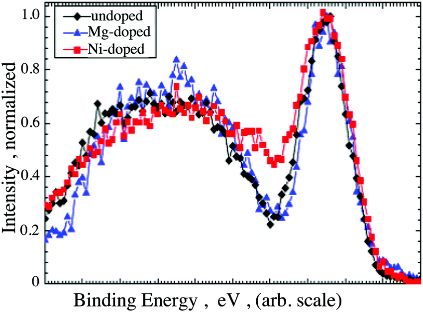 | ||
| Fig. 9 Comparison between the VB shape of an undoped, Mg-doped and Ni-doped Cr2O3 films. The graphs are shifted in order highlight the change in shape upon Ni-doping. | ||
The electronic density of states (EDOS) were generated with DFT to examine the influence of Ni and Mg on the VB. The total and partial EDOS of undoped, Mg-doped, and Ni-doped Cr2O3 are shown in Fig. 10. Notably, there is no interaction of the valence Mg s states with the VB of the host system as they are significantly lower in energy, while in the Ni-doped system, the Ni d states are present in the VB where they can mix with the O 2p states. This is in good agreement with the experimentally obtained XPS data, as the Ni 3d states occupy the energetic range of zero density observed in the Mg-doped system between 1 eV and 2 eV.
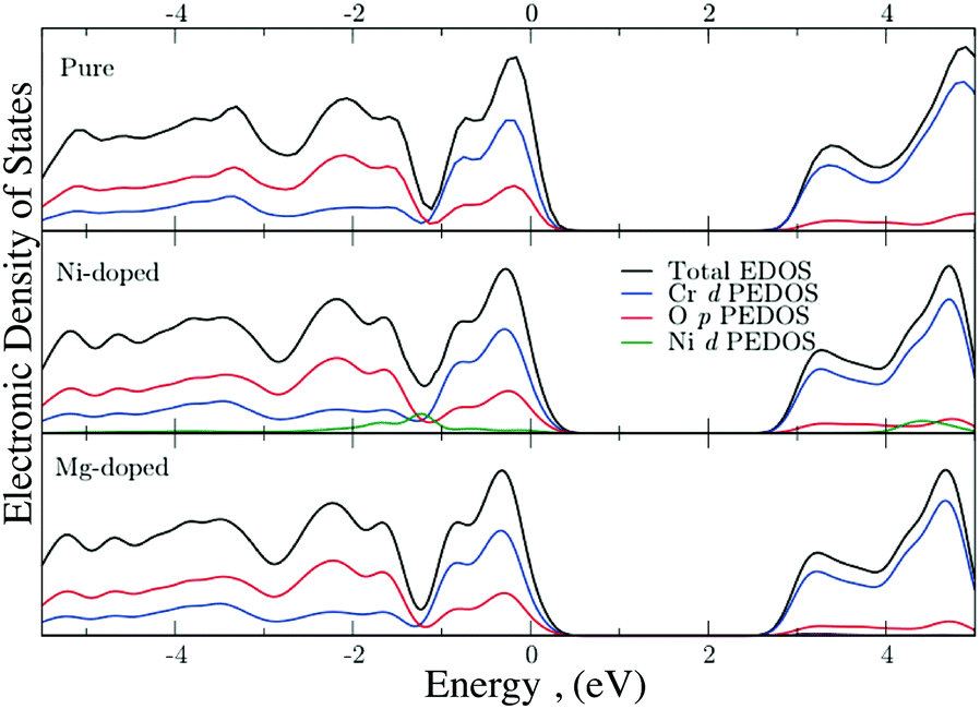 | ||
| Fig. 10 Total and partial EDOS of (a) undoped, (b) Ni-doped and (c) Mg-doped Cr2O3. The top of the VB is aligned to 0 eV in all cases. | ||
5 Discussion
Experimentally, it was demonstrated that Ni incorporation in Cr2O3 produces films with considerably higher conductivities than Mg-doped films, achieving values of 28 S cm−1, which is higher than any Cr2O3 doped films previously reported in the literature. TCOs are often assessed using a ratio of electrical conductivity to visible absorption coefficient known as the figure of merit, calculated from the sheet resistance, total visible transmission, and total visible reflectance.68 The figure of merit determined here for Ni-doped Cr2O3 is 110 MΩ−1. For comparison, the best n-type materials typically have values on the order of 1 Ω−1, while other prospective p-type materials such as CuCrO2:Mg, Bi2Sr2Co2Oy, LaSr0.25Cr0.75O3 and LaSr0.5Cr0.5O3 have figures of merit of 4600 MΩ−1,12 800 MΩ−1,13 196 MΩ−1,14 and 314 MΩ−1,14 respectively. Indeed, LaSr0.25Cr0.75O3, despite not having the highest figure of merit, was recently claimed as the best p-type TCO based on the compromise between optical transparency and electrical conductivity.To explain the improved conductivity of Ni-doped samples over Mg-doping, electrical measurements, structural characterization, spectroscopic measurements, and DFT calculations were performed. DFT calculations of the EDOS and experimentally determined XPS show a contribution of the Ni d-levels to the valence band, whereas Mg electronic levels do not contribute to it. The presence of Ni d-levels helps the delocalization of the formed holes, thus reducing the hole effective mass. The importance of a second cation in the formation of the VB and on the delocalization of the holes has been already proven for the case of CuCrO2, where the effect is even more pronounced. Similar to the combination of Cu2O's conductivity and the transparency of Cr2O3 in delafossite p-type TCO CuCrO2, we propose that combining transparent insulator Cr2O3 with semiconductor NiO can result in mixing of their valence bands to produce a viable p-type TCO, something that MgO, itself an insulator, cannot achieve when mixed with Cr2O3.
In the case of the Ni-doped films, the improvement in hole delocalization is just a partial explanation for the increased conductivity. The second reason for such an improvement arises from the doping level. Mg has a limited solubility in Cr2O3: 6.6 at% cation substitution appears to be the maximum achievable, and any attempt to increase its concentration, either by varying the temperature or by increasing the Mg content in the target, resulted in phase separation. Conversely, Ni can be present in a considerably higher concentration (almost a factor of 3) without inducing phase separation. This high solubility is achieved by reducing the deposition temperature to a point where spurious phases are disfavored and the crystal quality of the Cr2O3 host-matrix is preserved. From a thermodynamic point of view, it would be expected that Mg and Ni should have comparable solubility, considering that DFT calculations show comparable formation energy. However, it has been shown that for some systems, non-equilibrium growth conditions can induce a considerable increase in the solubility of dopants, generating metastable compositions.69–71 At very high doping concentrations, the Ni atoms are prone to aggregate. This is clearly shown in the modulation of the Ni distribution in the Cr2O3 lamella, with layers of higher and lower Ni concentration that develop along the c-axis, further supported by the DFT calculations, which show that the system with all the dopant positioned close to each other has a lower energy than the system where the dopant atoms are homogeneously distributed.
6 Conclusion
A complementary experimental and theoretical investigation has been adopted to compare the potential of Mg- and Ni-doped Cr2O3 as p-type TCOs and to rationalise the observed higher conductivity of the Ni-doped samples over the Mg-doped. It was found that Ni is very effective p-type dopant in Cr2O3, capable of reaching conductivities of 28 S cm−1. Both theoretical and experimental data has demonstrated that one of the major differences between the two dopants is the capability of Ni to contribute to the VB, contrary to Mg, whose electronic levels lie too deep. Ni contribution to the VB induces better delocalization of the formed holes and thus a lower effective mass. Formation energies and transition levels for a p-type defect whereby Ni/Mg replace a Cr atom in the structure are very similar in both cases and thus one could expect similar acceptor concentrations. However, it has been experimentally shown that Ni has a much higher solubility in Cr2O3 than Mg under certain non-equilibrium conditions, and its concentration is almost three times higher. The mixing of Ni states with the VB of the host material and the concomitant increase in the dopant concentration explain the improvement in the electrical properties of the material.Authors contribution
E. A. designed and synthesized the material, performed structural, optical and electrical measurements; A. B. K., D. O. S., G. W. W. performed the DFT calculations; T. D. V. performed the XPS analysis; A. S., C. D., D. D., V. N. performed the TEM and EDX analysis; D. M., I. V. S. contributed to the electrical measurements.Conflicts of interest
There are no conflicts to declare.Acknowledgements
This research was supported by SFI through the PI programme (grant numbers 12/IA/1414 and SFI12/IA/1264). E. Arca acknowledges SFI for the Advance Award Fellowship (grant number SFI14/ADV/IA2641). T. D. Veal acknowledges support from the EPSRC (grant no. EP/N015800/1). D. O. Scanlon acknowledges the EPSRC grant number EP/N01572X/1. V. Nicolosi, A. Shmeliov, D. Daly and C. Downing acknowledge SFI infrastructure funding for the NION UltraSTEM 200 and AMBER centre. Calculations were performed on ARCHER via membership of the Materials Chemistry Consortium (funded by EPSRC grant number EP/L000202), the DJEI/DES/SFI/HEA Irish Centre for High-End Computing (ICHEC) platform Fionn (project tcche056b), and the Lonsdale and Kelvin clusters maintained by TCHPC.References
- D. P. D. Ginley and H. Hosono, Handbook of transparent conductors, Springer, New York, 2010 Search PubMed.
- A. Klein, J. Am. Ceram. Soc., 2013, 96, 331–345 CAS.
- J. Robertson, R. Gillen and S. J. Clark, Thin Solid Films, 2012, 520, 3714–3720 CrossRef CAS.
- A. Stadleremail, Materials, 2012, 5, 661–683 CrossRef PubMed.
- S. Sallis, D. O. Scanlon, S. C. Chae, N. F. Quackenbush, D. A. Fischer, J. C. Woicik, J.-H. Guo, S. W. Cheong and L. F. J. Piper, Appl. Phys. Lett., 2013, 103, 042105 CrossRef.
- D. O. Scanlon and G. W. Watson, J. Phys. Chem. Lett., 2010, 1, 3195–3199 CrossRef CAS.
- A. Walsh, J. L. F. Da Silva, S. H. Wei, C. Korber, A. Klein, L. F. J. Piper, A. DeMasi, K. E. Smith, G. Panaccione, P. Torelli, D. J. Payne, A. Bourlange and R. G. Egdell, Phys. Rev. Lett., 2008, 100, 167402 CrossRef PubMed.
- N. F. Quackenbush, J. P. Allen, D. O. Scanlon, S. Sallis, J. A. Hewlett, A. S. Nandur, B. Chen, K. E. Smith, C. Weiland, D. A. Fischer, J. C. Woicik, B. E. White, G. W. Watson and L. F. J. Piper, Chem. Mater., 2013, 25, 3114–3123 CrossRef CAS.
- A. Zunger, Appl. Phys. Lett., 2003, 83, 57–59 CrossRef CAS.
- J. Robertson and S. J. Clark, Phys. Rev. B: Condens. Matter Mater. Phys., 2011, 83, 075205 CrossRef.
- A. Walsh, J. Buckeridge, C. R. A. Catlow, A. J. Jackson, T. W. Keal, M. Miskufova, P. Sherwood, S. A. Shevlin, M. B. Watkins, S. M. Woodley and A. A. Sokol, Chem. Mater., 2013, 25, 2924–2926 CrossRef CAS.
- R. Nagarajan, A. D. Draeseke, A. W. Sleight and J. Tate, J. Appl. Phys., 2001, 89, 8022–8025 CrossRef CAS.
- R. Wei, X. Tang, L. Hu, Z. Hui, J. Yang, H. Luo, X. Luo, J. Dai, W. Song, Z. Yang, X. Zhu and Y. Sun, Chem. Commun., 2014, 50, 9697–9699 RSC.
- K. H. L. Zhang, Y. Du, A. Papadogianni, O. Bierwagen, S. Sallis, L. F. J. Piper, M. E. Bowden, V. Shutthanandan, P. V. Sushko and S. A. Chambers, Adv. Mater., 2015, 27, 5191–5195 CrossRef CAS PubMed.
- M. O'Sullivan, P. Stamenov, J. Alaria, M. Venkatesan and J. M. D. Coey, J. Phys.: Conf. Ser., 2010, 200, 052021 CrossRef.
- A. R. Nagaraja, N. H. Perry, T. O. Mason, Y. Tang, M. Grayson, T. R. Paudel, S. Lany and A. Zunger, J. Am. Ceram. Soc., 2012, 95, 269–274 CrossRef CAS.
- G. Hautier, A. Miglio, G. Ceder, G.-M. Rignanese and X. Gonze, Nat. Commun., 2013, 4, 2292 Search PubMed.
- B. J. Ingram, B. J. Harder, N. W. Hrabe, T. O. Mason and K. R. Poeppelmeier, Chem. Mater., 2004, 16, 5623–5629 CrossRef CAS.
- B. J. Ingram, T. O. Mason, R. Asahi, K. T. Park and A. J. Freeman, Phys. Rev. B: Condens. Matter Mater. Phys., 2001, 64, 155114 CrossRef.
- G. J. Exarhos, C. F. Windisch Jr, K. F. Ferris and R. R. Owings, Appl. Phys. A: Mater. Sci. Process., 2007, 89, 9–18 CrossRef CAS.
- K. G. Godinho, B. J. Morgan, J. P. Allen, D. O. Scanlon and G. W. Watson, J. Phys.: Condens. Matter, 2011, 23, 334201 CrossRef CAS PubMed.
- E. Fortunato, B. Raquel, B. Pedro, F. Vitor, P. Sang-Hee Ko, H. Chi-Sun and M. Rodrigo, Appl. Phys. Lett., 2010, 97, 052105 CrossRef.
- H. Hosono, Y. Ogo, H. Yanagi and T. Kamiya, Electrochem. Solid-State Lett., 2011, 14, H13–H16 CrossRef CAS.
- H. Kawazoe, M. Yasukawa, H. Hyodo, M. Kurita, H. Yanagi and H. Hosono, Nature, 1997, 389, 939–942 CrossRef CAS.
- R. Nagarajan, N. Duan, M. K. Jayaraj, J. Li, K. A. Vanaja, A. Yokochi, A. Draeseke, J. Tate and A. W. Sleight, Int. J. Inorg. Mater., 2001, 3, 265–270 CrossRef CAS.
- H. Kawazoe, H. Yanagi, K. Ueda and H. Hosono, MRS Bull., 2000, 25, 28–36 CrossRef CAS.
- A. Kudo, H. Yanagi, H. Hosono and H. Kawazoe, Appl. Phys. Lett., 1998, 73, 220–222 CrossRef CAS.
- K. G. Godinho, G. W. Watson, A. Walsh, A. J. H. Green, D. J. Payne, J. Harmer and R. G. Egdell, J. Mater. Chem., 2008, 18, 2798–2806 RSC.
- X. Nie, S.-H. Wei and S. B. Zhang, Phys. Rev. Lett., 2002, 88, 066405 CrossRef PubMed.
- M.-S. Miao, S. Yarbro, P. T. Barton and R. Seshadri, Phys. Rev. B: Condens. Matter Mater. Phys., 2014, 89, 045306 CrossRef.
- P. T. Barton, R. Seshadri, A. Knoller and M. J. Rosseinsky, J. Phys.: Condens. Matter, 2012, 24, 016002 CrossRef PubMed.
- H. Hiramatsu, K. Ueda, H. Ohta, M. Hirano, T. Kamiya and H. Hosono, Appl. Phys. Lett., 2003, 82, 1048–1050 CrossRef CAS.
- H. Hiramatsu, K. Ueda, H. Ohta, M. Hirano, M. Kikuchi, H. Yanagi, T. Kamiya and H. Hosono, Appl. Phys. Lett., 2007, 91, 012104 CrossRef.
- K. Ueda, S. Inoue, S. Hirose, H. Kawazoe and H. Hosono, Appl. Phys. Lett., 2000, 77, 2701–2703 CrossRef CAS.
- D. O. Scanlon, J. Buckeridge, C. R. A. Catlow and G. W. Watson, J. Mater. Chem. C, 2014, 2, 3429–3438 RSC.
- M. Dekkers, G. Rijnders and D. H. A. Blank, Appl. Phys. Lett., 2007, 90, 021903 CrossRef.
- J. D. Perkins, T. R. Paudel, A. Zakutayev, P. F. Ndione, P. A. Parilla, D. L. Young, S. Lany, D. S. Ginley, A. Zunger, N. H. Perry, Y. Tang, M. Grayson, T. O. Mason, J. S. Bettinger, Y. Shi and M. F. Toney, Phys. Rev. B: Condens. Matter Mater. Phys., 2011, 84, 205207 CrossRef.
- A. R. Nagaraja, K. H. Stone, M. F. Toney, H. Peng, S. Lany and T. O. Mason, Chem. Mater., 2014, 26, 4598–4604 CrossRef CAS.
- D. O. Scanlon and G. W. Watson, Phys. Chem. Chem. Phys., 2011, 13, 9667–9675 RSC.
- J. Im, G. Trimarchi, H. Peng, A. J. Freeman, V. Cloet, A. Raw and K. R. Poeppelmeier, J. Chem. Phys., 2013, 138, 194703 CrossRef PubMed.
- V.-A. Ha, F. Ricci, G.-M. Rignanese and G. Hautier, J. Mater. Chem. C, 2017, 5, 5772–5779 RSC.
- E. Arca, K. Fleischer and I. V. Shvets, Appl. Phys. Lett., 2011, 99, 111910 CrossRef.
- E. Arca, K. Fleischer, S. A. Krasnikov and I. Shvets, J. Phys. Chem. C, 2013, 117, 21901–21907 CAS.
- F. Lebreau, M. M. Islam, B. Diawara and P. Marcus, J. Phys. Chem. C, 2014, 118, 18133–18145 CAS.
- E. Arca, M. A. McInerney and I. V. Shvets, J. Phys.: Condens. Matter, 2016, 28, 224004 CrossRef PubMed.
- A. B. Kehoe, E. Arca, D. O. Scanlon, I. V. Shvets and G. W. Watson, J. Phys.: Condens. Matter, 2016, 28, 125501 CrossRef PubMed.
- J. J. Carey and M. Nolan, J. Mater. Chem. A, 2017, 5, 15613–15630 CAS.
- A. Atkinson, M. R. Levy, S. Roche and R. A. Rudkin, Solid State Ionics, 2006, 177, 1767–1770 CrossRef CAS.
- A. Holt and P. Kofstad, Solid State Ionics, 1999, 117, 21–25 CrossRef CAS.
- F. Maldonado, C. Novillo and A. Stashans, Chem. Phys., 2012, 393, 148–152 CrossRef CAS.
- A. N. Blacklocks, A. Atkinson, R. J. Packer, S. L. P. Savin and A. V. Chadwick, Solid State Ionics, 2006, 177, 2939–2944 CrossRef CAS.
- A. Holt and P. Kofstad, Solid State Ionics, 1997, 100, 201–209 CrossRef CAS.
- N. Uekawa and K. Kaneko, J. Phys. Chem., 1996, 100, 4193–4198 CrossRef CAS.
- G. M. Crosbie, G. J. Tennenhouse, R. P. Tischer and H. S. Wroblowa, J. Am. Ceram. Soc., 1984, 67, 498–503 CrossRef CAS.
- G. Kresse and J. Hafner, Phys. Rev. B: Condens. Matter Mater. Phys., 1994, 49, 14251–14271 CrossRef CAS.
- G. Kresse and J. Furthmüller, Comput. Mater. Sci., 1996, 6, 15–50 CrossRef CAS.
- G. Kresse and J. Furthmüller, Phys. Rev. B: Condens. Matter Mater. Phys., 1996, 54, 11169–11186 CrossRef CAS.
- J. P. Perdew, K. Burke and M. Ernzerhof, Phys. Rev. Lett., 1996, 77, 3865–3868 CrossRef CAS PubMed.
- S. L. Dudarev, G. A. Botton, S. Y. Savrasov, C. J. Humphreys and A. P. Sutton, Phys. Rev. B: Condens. Matter Mater. Phys., 1998, 57, 1505–1509 CrossRef CAS.
- A. M. Ferrari, C. Pisani, F. Cinquini, L. Giordano and G. Pacchioni, J. Chem. Phys., 2007, 127, 174711 CrossRef PubMed.
- A. B. Kehoe, D. O. Scanlon and G. W. Watson, Chem. Mater., 2011, 23, 4464–4468 CrossRef CAS.
- C. Freysoldt, J. Neugebauer and C. G. V. de Walle, Phys. Rev. Lett., 2009, 102, 016402 CrossRef PubMed.
- P. H. Fang and W. S. Brower, Phys. Rev., 1963, 129, 1561 CrossRef CAS.
- M. W. Cho, A. Setiawan, H. J. Ko, S. K. Hong and T. Yao, Semicond. Sci. Technol., 2005, 20, S13–S21 CrossRef CAS.
- O. Durand, A. Letoublon, D. J. Rogers and F. Hosseini Teherani, Thin Solid Films, 2011, 519, 6369–6373 CrossRef CAS.
- R. D. Shannon, Acta Crystallogr., Sect. A: Cryst. Phys., Diffr., Theor. Gen. Crystallogr., 1976, 32, 751–767 CrossRef.
- A. Subramaniyan, J. D. Perkins, R. P. O'Hayre, D. S. Ginley, S. Lany and A. Zakutayev, J. Mater. Sci., 2014, 50, 1350–1357 CrossRef.
- R. G. Gordon, MRS Bull., 2000, 25, 52–57 CrossRef CAS.
- A. Zakutayev, V. Stevanovic and S. Lany, Appl. Phys. Lett., 2015, 106, 123903 CrossRef.
- A. K. Sharma, J. Narayan, J. F. Muth, C. W. Teng, C. Jin, A. Kvit, R. M. Kolbas and O. W. Holland, Appl. Phys. Lett., 1999, 75, 3327–3329 CrossRef CAS.
- H. Peng, P. F. Ndione, D. S. Ginley, A. Zakutayev and S. Lany, Phys. Rev. X, 2015, 5, 021016 Search PubMed.
Footnotes |
| † Electronic supplementary information (ESI) available. See DOI: 10.1039/c7tc03545d |
| ‡ Present address: National Renewable Energy Laboratory, 15013 Denver West Parkway, Golden, Colorado 80401, USA. |
| This journal is © The Royal Society of Chemistry 2017 |