Two-dimensional GaGeTe film: a promising graphene-like material with tunable band structure and high carrier mobility†
Abstract
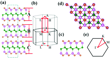
Exploring experimentally feasible two-dimensional (2D) films with high carrier mobility and tunable band structure is one key to developing next-generation nanodevices. Motivated by successful synthesis of the layered GaGeTe in previous experiments, we performed first-principles calculations to explore the geometric and electronic properties of GaGeTe few-layers, with a focus on the monolayer. The interlayer interaction in layered GaGeTe was found to be rather weak, with a cleavage energy of 0.53 J m−2, suggesting that the exfoliation of bulk crystal is a viable means for the preparation of GaGeTe few-layers. When thinned from bulk to few-layers, a transition from semimetal to semiconductor occurs with a band gap in the range of 0–0.74 eV, which is promising for the photovoltaic emitting devices. Moreover, the indirect band gap of the GaGeTe monolayer can be effectively tuned by applying mechanical strain and decreases with increasing tensile strain, while it increases and turns into a direct band gap under a compressive strain of 2.0%. Anisotropic carrier mobility can be observed along zigzag and armchair directions of the GaGeTe monolayer, and particularly for the former, a maximum of 7.83 × 104 cm2 V−1 s−1 was observed. Considering that the GaGeTe monolayer is both dynamically and thermodynamically stable at a temperature of 600 K, these findings expand the potential applications of the emerging field of 2D germanene-based crystals in nanoelectronics.


 Please wait while we load your content...