
 Open Access Article
 This Open Access Article is licensed under a
 Creative Commons Attribution 3.0 Unported Licence
3D reactive inkjet printing of polydimethylsiloxane†
Craig
Sturgess
 ,
Christopher J.
Tuck
,
Ian A.
Ashcroft
and
Ricky D.
Wildman
*
,
Christopher J.
Tuck
,
Ian A.
Ashcroft
and
Ricky D.
Wildman
*
Faculty of Engineering, Department of Mechanical, Materials and Manufacturing Engineering, University of Nottingham, Nottingham, NG7 2RD, UK. E-mail: Ricky.Wildman@Nottingham.ac.uk
First published on 21st August 2017
Abstract
Material jetting is a process whereby liquid material can be deposited onto a substrate to solidify. Through a process of progressive additional layers, this deposition can then be used to produce 3D structures. However, the current material jetting catalogue is limited owing to the constraints on the viscosity of inks that can be deposited. Most inks currently being used are either solvent or photocuring based, with the latter becoming increasingly popular due to increased throughput. Full Reactive Inkjet Printing (FRIJP) is an alternative processing method currently being investigated as a route to widen the material catalogue. FRIJP is the combination, on the substrate, of two reactive components which then react together in contact on the substrate. In this work a two-part polydimethylsiloxane (PDMS) ink has been developed, printed individually, and cured. The successful printing of PDMS has been used to fabricate complex 3D geometry for the first time using FRIJP. Through the use of a prepared substrate feature resolutions up to 48 ± 2 μm (X, Y) were possible. Curing analysis has been conducted. It was found that not only does the reaction occur to a similar degree to conventional processes, but that there is no variation in the cured sample when printed at elevated substrate temperatures.
Introduction
Additive Manufacturing (AM) is a method for producing complex and bespoke designs from digital data without the need for tooling or moulds.1,2 The key to achieving this is fabrication through the layer-wise addition of material. There are a number of different technologies under the umbrella of AM, including: powder bed fusion,3 material extrusion,4 photo-lithography,5 binder jetting,5 sheet lamination,5 and material jetting.6 An advantage of material jetting over powder bed systems is the capability to easily incorporate multiple materials within the same structure in a fully 3D array. Examples include, combinations of hard and soft materials, electrically conducting and insulating polymers7 and biomaterial components.8 This multi-material capability enables extended functionality compared with traditional single material AM. Coupled with the ease of co-deposition and the high scalability of the process, this makes jetting an enabling manufacturing process for the future.The extension of inkjet printing technology into 3D printing presents numerous challenges. Currently, the range of inkjet materials suitable for AM is limited. Previous research has focused on creating inks suitable for 2D deposition, where the layer thickness is unimportant and material loading can be low.9 For 3D Printing, the volumetric throughput is related to the layer thickness achievable given the functional loading of the ink. Initial approaches relied on loading solvents with nanoparticles10 or polymer,11–13 and evaporating the solvent to leave the desired solid. Newer approaches using photocurable14 and phase change materials15 offer substantially increased volumetric throughput in comparison, but are still limited in their material range. A further alternative is to combine reactive components to form the desired material during the manufacturing process itself.16 This fully reactive inkjet printing (FRIJP) inherits the advantages of inkjet printing, including sub-micron scale droplet positioning, sub-femtolitre volume control,17 and high processing speeds,7 whilst broadening the palette of materials available for additive manufacturing. Such a multi-component method has been demonstrated for the case of addition polymerisation to produce a polyurethane polymer,18 in the formation of nylon,19 and the reduction of metals, such as copper.20 Through this method, liquid droplets can be processed without chemical modification or external initiating steps.
Polydimethylsiloxane (PDMS) is a silicone elastomer that is widely used due to its low cost, biocompatibility, and optical transparency. One principle use of PDMS is the fabrication of microfluidic devices.21 The transparency of PDMS in visible light has led to developments in integrated optics;22 where optical waveguides have been fabricated that show mechanical compatibility with microfluidic channels and low attenuation losses.23–25 PDMS has also shown interesting properties when printing conductive tracks, for both adhesion of the ink and flexibility of the part.26 Recently, organosilicon self-assembled layers have been processed through reactive inkjet printing.27 However, despite these developments, a method for directly inkjet printing controlled PDMS structures has not been demonstrated.
Despite the lack of material jetting for PDMS fabrication, there has been some work with other additive manufacturing methods. Through the use of a supporting bath PDMS structures have been printed,28 after printing the bath medium acts a support for extended curing times and can be removed with a phosphate buffered saline solution. A multi-head extrusion system has demonstrated the printing of dyed premixed PDMS.29 The PDMS is extruded through a nozzle of 200 μm for use in vascular representations. The non-contact dispensing of premixed PDMS has been used for single droplet fabrication of lenses.30 Material jetting as a method has several advantages over material extrusion as discussed above, but the main ones are the ability to produce smaller features and a more scalable manufacturing method. An advantage specific to FRIJP is the ability to mix materials on the substrate, removing the need to mix reactive components before printing. The mixing on the substrate allows for faster curing components, able to fully cure at lower temperatures. These materials are then kept in a stable form inside the printing system. It also allows for the ability to vary the mixing ratio during printing, facilitating functional grading of parts.
In this paper a method for the multiple component reactive inkjet printing of PDMS structures is proposed. Two methods were considered. First, the reactants were deposited in complete layers, which led to the components, A and B, being printed with a separation of around two minutes. The second method used an improved strategy whereby both components were printed in a single pass. This reduced the delay between printing the PDMS components to around 0.3 s. The effect of the surface energy of the substrate on the wetting of the first layer of material was considered, as well as the development of a strategy for combining reactants and producing PDMS objects. Finally, the successful printing of an object and its subsequent characterisation will be used to demonstrate the approach as a method for 3D printing.
Method
Materials and printing
A commercially available two-part silicone (Polytek PlatSil 71-Silliglass) was used as the basis of a reactive ink. The viscosities of the reactants (155 mPa s and 200 mPa s) were sufficiently close to the operating range of industrial print heads to allow for high polymer loading in a solvent. The two parts of the PDMS ink are referred to as A (hydride containing) and B (catalyst containing), and the reaction is shown in Fig. 1. The formulation consists of a 1![[thin space (1/6-em)]](https://www.rsc.org/images/entities/char_2009.gif) :1 (weight) ratio of A to B, where the silicone is crosslinked in the presence of a platinum catalyst (transported in ink B). The reaction is not inhibited by oxygen or moisture, and as a consequence can be carried out without a controlled atmosphere.
:1 (weight) ratio of A to B, where the silicone is crosslinked in the presence of a platinum catalyst (transported in ink B). The reaction is not inhibited by oxygen or moisture, and as a consequence can be carried out without a controlled atmosphere.
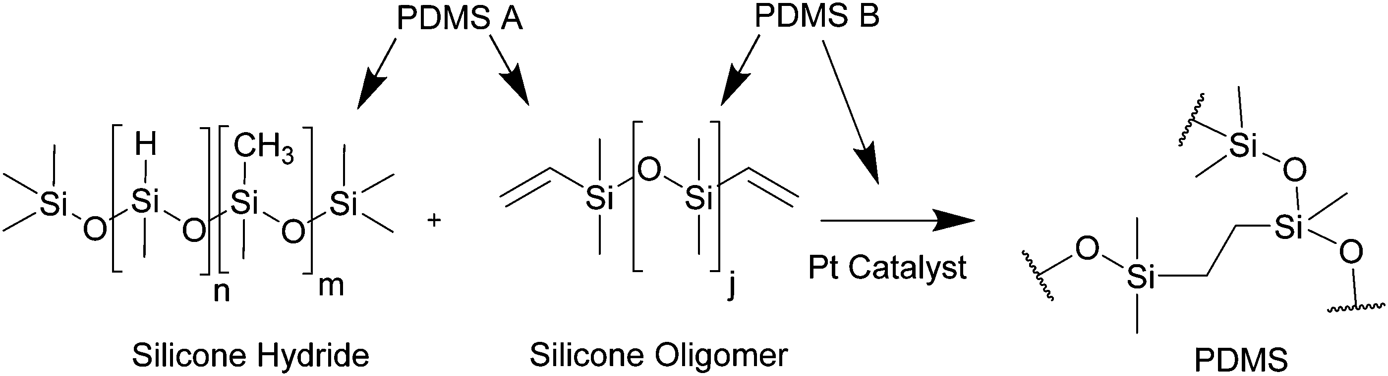 | ||
| Fig. 1 Crosslink reaction of PDMS in the presence of a platinum catalyst, the silicone hydride bond Si–H is replaced with an additional Si–C bond. Labelled are the compounds in each component of the PDMS formulation. | ||
The advised operating range of the Dimatix Material Print head (DMP) (Dimatix, Fujifilm) employed for the printing is 10–12 mPa s and 28–33 mN m−1 for viscosity and surface tension respectively, but it is stated that viscosities as high as 30 mPa s and surface tensions up to 70 mN m−1 may be used.31 Two jettable inks were produced by creating 60 wt% solutions of PDMS A and B using octyl acetate (OA) as a viscosity modifier (Sigma Aldrich; O5500). This solvent was chosen as it was miscible with the PDMS formulations and offered a suitable vapour pressure for printing. The solutions were miscible and stable during formulation and printing. To further tune the viscosity, print head heating was used.
Ink viscosity was determined using a concentric cylinder rheometer (Malvern Kinexus Pro) with a shear rate sweep between 1 s−1 and 1000 s−1 and a temperature ramp between 20 °C and 70 °C. The ink formulation was judged to be printable when the viscosity was under the 30 mPa s threshold; further heating was found to achieve an ink viscosity below 20 mPa s at 60 °C. An important factor in inkjet printing, and also on how ink droplets form on the substrate, is the ink interfacial tension which was determined through the pendant drop method with a drop shape analyser (KRUSS DSA 100). It was found, however, that while the surface tension was inside the printable range, it was lower than the ideal range. The values for the viscosity and surface tension, for the PDMS components, solvent, and final inks are presented in Table 1.
| Fluid | Viscosity (mPa s) 20 °C | Viscosity (mPa s) 60 °C | Interfacial tension (mN m−1) | Droplet mass (ng) |
|---|---|---|---|---|
| a Material MSDS. | ||||
| PDMS A | 155a | 95.6 ± 0.6 | — | |
| PDMS B | 200a | 74.8 ± 2.1 | — | |
| Octyl acetate | 1.8533 | — | 27.833 | |
| Ink A: OA (60% loading) | 38.2 ± 1.3 | 19.7 ± 0.25 | 23.6 ± 0.25 | 10.4 ± 0.24 |
| Ink B: OA (60% loading) | 34.0 ± 0.1 | 17.7 ± 0.12 | 23.3 ± 0.13 | 11.92 ± 0.18 |
From the work of Reis32 it is understood that droplet volumes can be affected by a number of factors: ink viscosity, ink surface tension, and nozzle dimensions. This meant that despite the similar parameters associated with the A and B inks, differences were to be expected in droplet volume. This variation would then affect mixing ratio and the final curing. To accommodate this, firstly 100000 droplets were printed into a low weight metal pan and weighed, and then the obtained mass was used to change the droplet ratio during printing. Droplet masses were found to be 10.4 ng and 11.92 ng for ink A and B respectively.
FRIJP process
Inkjet printing was carried out using an in-house printing system. Two DMP cartridges each with 16 nozzles were driven with an arbitrary function generator AFG3252C (Tektronix, USA) and amplified to 30 V. The heads were positioned and fired using a PixDro LP50 (Roth&Rau, Netherlands) printer. The DMP cartridges have a closed loop thermal control system, which was used to maintain the head temperature at 60 °C.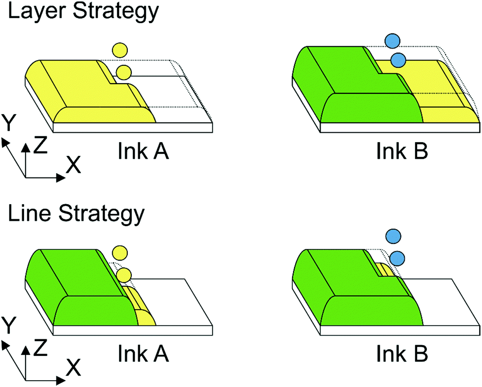 | ||
| Fig. 2 Process of FRIJP showing line print in the Y direction, with number of lines increasing in the X direction. Each ink is printed in series, first ink A (yellow), then ink B (blue) only when both inks are printed can the curing occur (green). Layers are counted in total reacted (green) layers printed. | ||
Substrates
Three material substrates were employed, standard glass slides, PTFE, and glass chemically modified with 1% 1H,1H,2H,2H-perfluoroctyltriethoxysilane (PFOTS) (Sigma Aldrich 667420) in anhydrous toluene.To create the PFOTS-glass the pre-cleaned glass slides were first treated with 70% nitric acid (Sigma Aldrich 438073). They were then rinsed with anhydrous toluene (Sigma Aldrich 568821). After drying they were chemically coated with the PFOTS solution overnight. They were once again rinsed with anhydrous toluene before being baked in an oven at 100 °C for 1 hour.
The contact angle of the prepared PDMS ink was evaluated against the substrates using the sessile drop method with a drop shape analyser (KRUSS DSA 100). It was found that both the PTFE and PFOTS produced a higher contact angle than that of glass. A final substrate, of the cured PDMS was analysed which showed increased wetting over the PTFE and PFOTS. The results of the contact angle, shown in Table 2, suggest that the best feature resolution would be possible using the PFOTS substrate.
Chemical analysis
Chemical analysis of the PDMS samples was conducted with two aims. The work involving the Raman spectroscopy was used to study spatial variation in the samples, while FTIR analysis was used to quantify bulk residual hydride density. Raman and FTIR peaks used to determine residual cross link component were: silicone hydride 913 cm−1 (Si–H bend), and siloxane at 488.6 cm−1 (Si–O–Si vibration).34 The last bond, siloxane, was used to calibrate the intensity of the captured waveform allowing the comparison of multiple samples. Along with the printed samples, PDMS calibration samples were cast directly onto CaF2 glass slides. Three weight concentrations 1:1, 2:1, and 3:1, A:B were selected to produce PDMS samples with an estimated, 0%, 33%, and 50% excess hydride respectively. Cast samples were mixed following manufacturer instructions and allowed to cure for 24 hours at room temperature.
Raman spectral analysis was used to investigate the spatially varying cure, using a Horiba–Jobin–Yvon LabRAM Raman microscope (HORIBA, Japan), with an excitation laser wavelength of 532 nm and a 600 lines mm−1 grating. The detector was a Synapse CCD detector. The Raman shift was calibrated using a Si(100) reference sample. Scans were conducted in the print direction (Y), transverse to the print direction (X) and through the printed depth (Z). The complete scan dimensions were 750 μm × 750 μm × 100 μm (X, Y, and Z).
The FTIR-ATR was conducted on a Frontier (Perkin Elmer, USA) system. The ATR accessory was exclusively used for all sample analysis. Scans were initially conducted from 4000 to 650 cm−1, at a resolution of 4 cm−1. Later scans reduced the range to 2500 cm−1, thereby increasing the scan speed without losing information. The resulting spectra were taken from the average of four scans corrected by a baseline. The analysis was conducted in both Perkin Elmer's Spectrum software and using MATLAB to perform curve fitting for determination of the peak area.
Profile analysis
The macroscale profiles of the printed patterns were captured using an Alicona Infinite Focus G5 (Alicona, UK) surface measurement device via focus variation. Typical samples prepared in this work were smooth and transparent, so could not be directly measured. Instead, a physical replica of the sample was created using AccuTrans replica PDMS. The PDMS works well because it has a colour variation that aids the software in resolving features.35Results and discussion
Process overview
The goal of this work was to determine a method, or range of methods, to achieve a final component that had comparable resolution, freedom of design, and complexity to a single component ink. The subsequent method of FRIJP described in this paper is demonstrated for the production of droplet grids, thin fluid films, and complex 3D patterns. The various methods of analysis conducted on the samples produced using the layer and line deposition methods can be seen in Table 3.| Printing scheme | Analysis type | Analysis aim |
|---|---|---|
| Layer | Optical microscopy | Determine how the liquid pinning can be improved through the microstructuring method. |
| Line | Optical microscopy | Determine the drop spacing suitable for FRIJP of PDMS using the line based method. |
| Line and layer | Profile analysis | Determine distribution of material across the printed sample. |
| Layer | Raman microscopy | To determine if there are concentration gradients in printed samples. |
| Line | FTIR-ATR | To determine the degree of cure in the FRIJP method. |
Substrate surface treatment
The ability of PDMS to spread on most material surfaces is desirable when using moulding techniques, but for inkjet printing it directly reduces the feature resolution. Three material substrates; glass, PTFE, and PFOTS-glass were used in this project to increase the printed resolution of features on the substrate. Contact angle measurements were conducted, but the most robust way of gauging substrate suitability was by printing a grid. Table 2 shows the results from contact angle measurements, and Fig. 3 shows the results of printing a disconnected grid.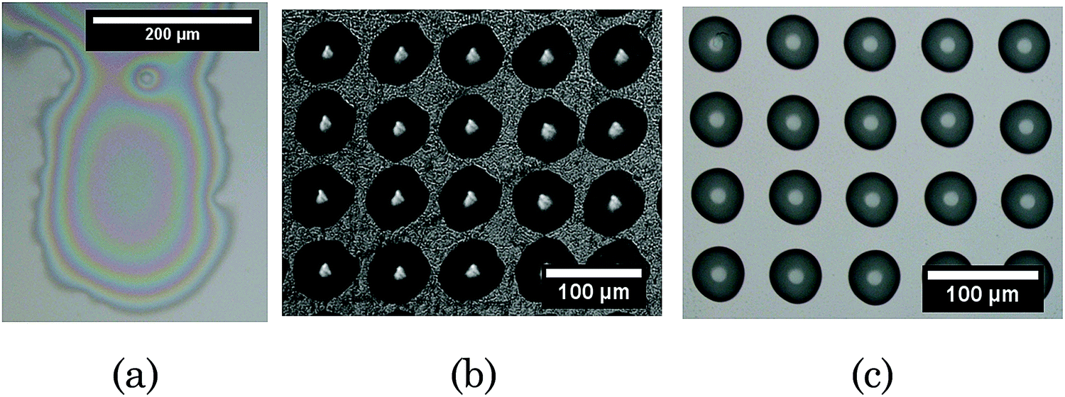 | ||
| Fig. 3 (a) The result of printing a single drop of ink A and B onto an untreated glass slide. (b and c) Showing printed grids composing both ink A and ink B onto (b) on a prepared PTFE coated slide and (c) PFOTS-glass. | ||
The printed grids in Fig. 3 show that the cleaned glass produced the largest droplet size, which was greater than 150 μm. The PFOTS-glass and PTFE had similar spot sizes, at 48 ± 2 μm, and 64 ± 2 μm respectively. The smaller and more circular drops on the PFOTS-glass were likely due to the decreased surface roughness. The ability to clean the PFOTS-glass, and the increased hardness over the PTFE meant that it was the selected substrate for continued work.
Stable films with layer printing
To inkjet print complex geometries, there needs to be a degree of stability in the printed areas on the substrate, i.e., the contact line should not move, keeping any structures in place whilst curing proceeds. This stability is a balance of three forces, the ink–substrate interaction (typical called pinning), the ink–air interfacial tension, and the force of gravity36,37 Printing stable lines with single inks typically involves selecting a suitable fluid volume to be deposited in an area through modification of the drop spacing. Typically, the inkjet printing of single inks benefits from relatively fast curing times, which reduces the need for prolonged ink–substrate stability. However, multiple inks printed using the layer strategy have an increased time before curing can occur, this is due to the initial requirement of depositing both reactive components. Once both inks are printed the curing process may also be slower due to the mixing that is involved. These factors mean that FRIJP inks need to have a greater stability, over a longer period, to produce the same geometry. It was found that with the PDMS ink in this work, the ink–substrate interaction was weak. This weak pinning, coupled with the long printing times, resulted in uncontrolled coalescence, as illustrated in Fig. 4.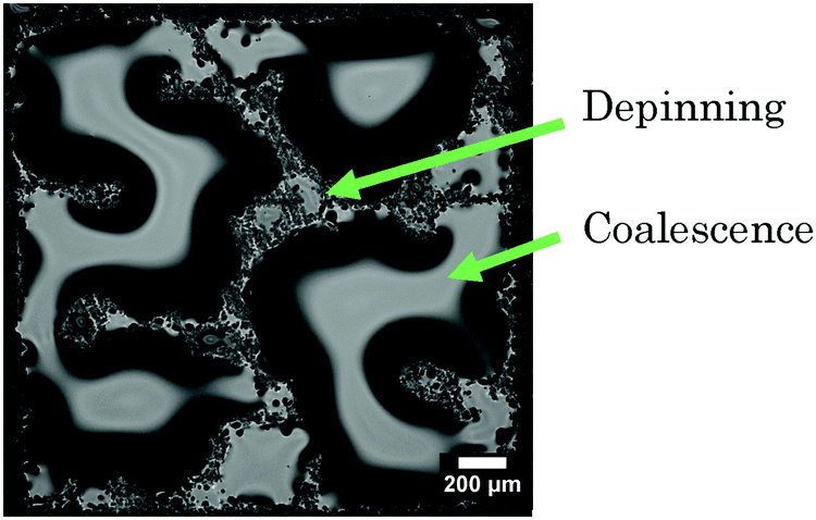 | ||
| Fig. 4 Microscope image of depinning and coalescence (labelled) present when the microstructuring pattern is not used, printed on to polished PTFE substrate heated to 80 °C. The intended pattern was a square, however liquid ink receded and bulged before curing could occur. | ||
To reduce the effect of uncontrolled liquid redistribution noted above, enhanced pinning between liquid–solid PDMS was investigated. The process used, termed microstructuring, involved the creation of pinning sites which act to increase the stability of any connected lines or films by creating an already established set of disconnected pinning sites. This method has been explored previously in regards to increasing solvent ink loading on a substrate.38Fig. 5 shows this process over a total of four reactive layers (eight printed layers). Initial spacing was set such that the first layer of the printed grid did not coalesce, only after the second layer of ink A was printed did coalescence occur. Once both components were printed the successive printing of layers resulted in a controlled coalescence. Finally, after four reactive layers the spreading was complete and complete coverage was achieved between the drops in the initially printed grid. This was accomplished with no undesired spreading outside the designated area.
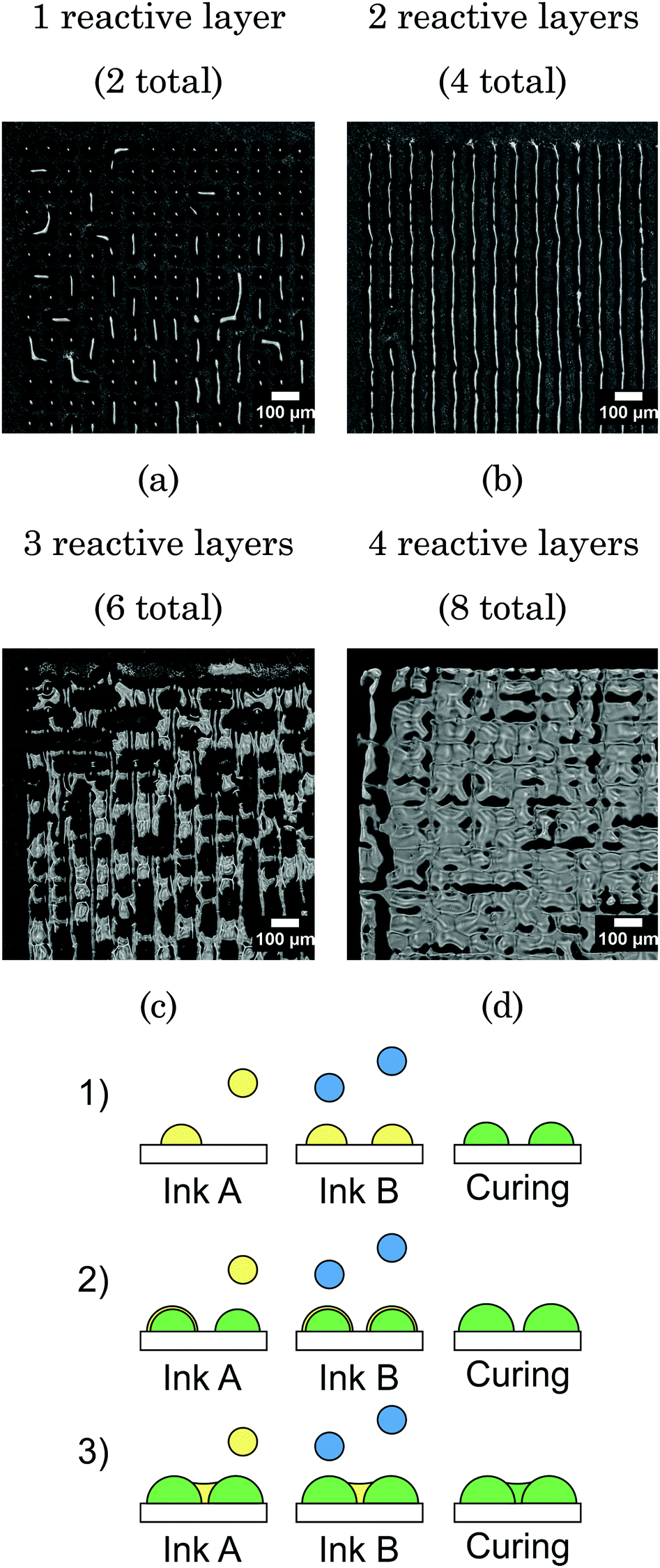 | ||
| Fig. 5 Substrate microstructuring, disconnected droplet printing to maximise the effect of pinning on a substrate where single PDMS ink does not pin. (a) A single layer of each component, ink A and B is deposited (shown in the schematic, phase 1), the initial spacing of the ink is such that the ink A does not coalesce. (b–d) Additional layers printed onto the grid, controlled spreading occurs (shown in the schematic, phase 2 for spreading, and phase 3 for bridging) and finally a continuous film is produced. | ||
Fig. 6 shows how this method is capable of producing continuous cured PDMS films with a high corner definition. Ultimately, the microstructuring method, along with substrate surface modification, allows for increased feature resolution and feature control.
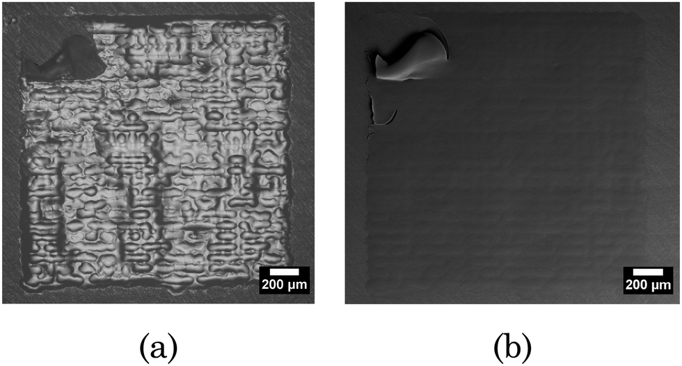 | ||
| Fig. 6 (a) Microscope (Nikon ECLIPSE LV100ND) image of a printed film, and (b) SEM (Hitachi Analytical Benchtop SEM TM3030) image of a printed film, sample platinum coated for 90 s, printed on a polished PTFE substrate heated to 80 °C. High sample waviness was caused by the initial microstructured film process, visible in the microscope image, the SEM image however. To confirm that the sample was a continous film the top left corner was peeled. | ||
The mechanism by which the microstructuring method works is similar to spin coating a substrate with a compatible polymer, but in this case the application of the microstructured pattern can afford greater control. This means it is possible to maintain the high feature resolution of the underlying substrate whilst increasing the pinning forces.
Once stable films were printed using the layer method, further layers were deposited to create thick films. In total 50 reactive layers, involving 50 layers of ink A and ink B, were deposited. The surface profiles of these films were then measured. The flatness of the top surface was of particular importance, since to build 3D structures, a known and repeatable layer thickness is required. It was expected that the long time to mixing would reduce flatness, but that the increased substrate temperature would mitigate this.
The results of the profile analysis are shown in Fig. 7. Differences in height profiles can be induced by altering the substrate temperature – for example, increasing the temperature from 40 °C to 60 °C shifts the profile from dome shaped, to one that is relatively flat. However, this uniformity is still subject to edge effects where material recedes from the outer edges. The layer height for these prints were; 12.1 ± 1.8 μm, 12.4 ± 1.4 μm, and 11.3 ± 1.9 μm for the sample printed at 40 °C, 60 °C, and 80 °C respectively. This height is calculated from the average and standard deviation of the heights across the total profile divided by the number of layers which was 50. This movement is known to be caused by the surface tension of the liquid, as discussed by Thompson.39 Further heating appears to maintain the same profile but increases the variation of material height throughout.
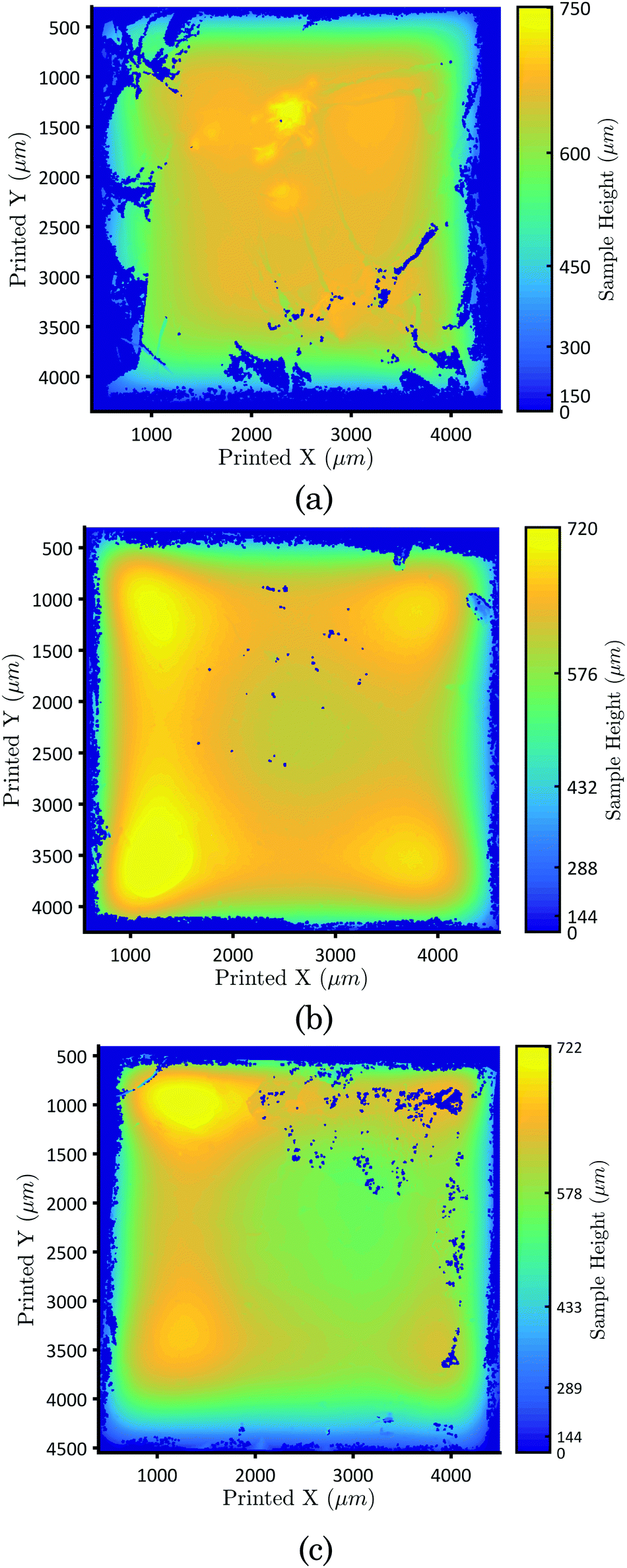 | ||
| Fig. 7 Profiles of the printed PDMS using the layer method with microstructuring and 50 reactive layers. (a) Printed at substrate temperature of 40 °C, (b) 60 °C, (c) 80 °C. Missing data is due to either high angles that are unscannable or the replication process causing incorrect replication. | ||
Printing line strategy
The microstructuring method was employed when the mixing and subsequent curing time was too long for stability to be achieved using the layer strategy, however, this approach was unnecessary when using the line strategy. With the removal of the microstructuring to achieve the desired geometry, it was possible to experimentally determine the lowest drop spacing that produced a stable line. To determine the suitable spacing for this ink system, a range of separations were printed and optically analysed. The follow separations were trialled: 30 μm, 35 μm, 40 μm, and 45 μm. These distances only controlled the spacing of ink A, whereas ink B was the product of the drop spacing and the mixing ratio. The corresponding spacings used for ink B were; 34.4 μm, 40.1 μm, 45.8 μm, and 52.6 μm; which were based on the mixing ratio from the droplet masses of A:B 1:0.87. The results of the drop spacing test are shown in Fig. 8.
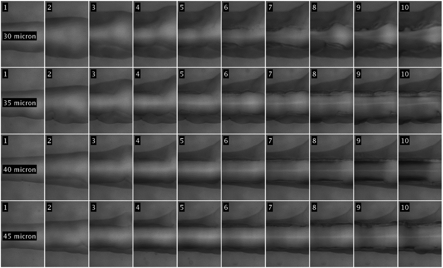 | ||
| Fig. 8 Determination of the minimum drop spacing for stable line formation of printed PDMS. Ten layers of five lines were printed at different drop spacings. | ||
To understand the stability of the printed layers within the context of AM, the performance of multiple layers was then assessed. To maximise printing speed, the lowest droplet separation that achieved stable lines was chosen. The line stability was judged by the line morphology variation over many layers. For example, the 30 μm spacing showed continual spreading on each layer. From the results of the line stability tests a primary drop spacing of 40 μm was selected for future printing.
Substrate microscopy was used to characterise the printed films, and during the printing process after every layer an image was captured of the bottom left corner. Fig. 9 shows the growth of the PDMS sample during the first five layers. The first layer is directly printed onto the PFOTS-glass, and due to the fast curing rate it does not recede. Successive layers print onto the PDMS film and build up the layers to create the 3D object.
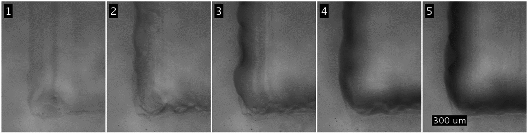 | ||
| Fig. 9 FRIJP Line strategy printing directly onto the PFOTS-glass. The substrate temperature is 80 °C. | ||
As a demonstration of capability to print a fully 3D object in PDMS, a stepped ziggurat design was printed (Fig. 10). The design contained five steps, each printed with 30 reactive layers. Profile analysis shows the layer heights were less than those created with the layer printing strategy at; 8.3 ± 1.9 μm, 7.3 ± 1.4 μm, 6.3 ± 2.1 μm, 7.5 ± 1.5 μm, and 6.8 ± 1.5 μm for the first to last layer respectively. This reduced layer height is expected as the line based method used an increased drop spacing. In example, this increased spacing over a fixed 4 mm square area would result in 19000 drops printed for the line strategy, versus 26000 for the layer one.
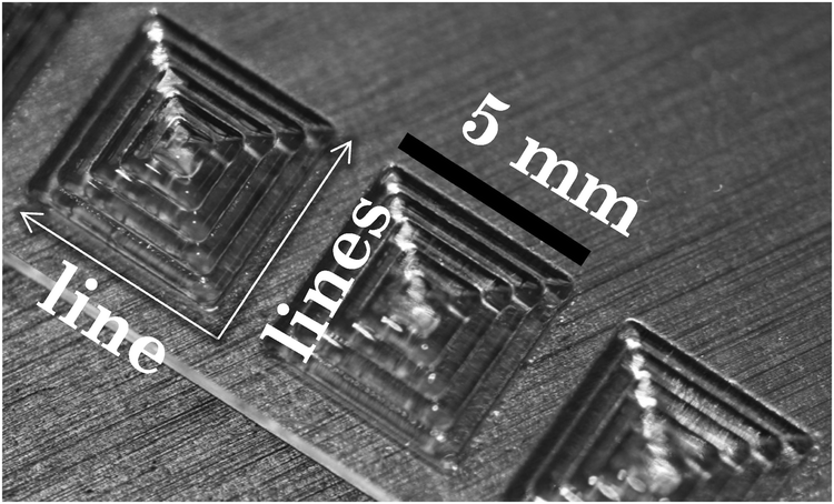 | ||
| Fig. 10 Stepped ziggurat, 4 × 4 mm PDMS consisting of 5 steps, each printed with 30 reactive layers. | ||
A consequence of the stepped ziggurat design was that it could be used to determine any effect of printed line length on the profile. For example, it can be seen in Fig. 11 in the Y (print) direction, increased scan length resulted in a more uniform layer height. The variation in this single sample is 17 μm for the first layer, increasing to 34 μm for the penultimate, shorter scan layer. The printing strategy in the layer based method is controlled so that each line printed takes the same amount of time, i.e. smaller printed patterns do not reduce the line scan time. Therefore, the only cause for this increased variation is due to a temperature gradient, where the sample on top is cooler than the bottom. The substrate was set to 80 °C and from previous results, reducing the substrate temperature led to increased variation.
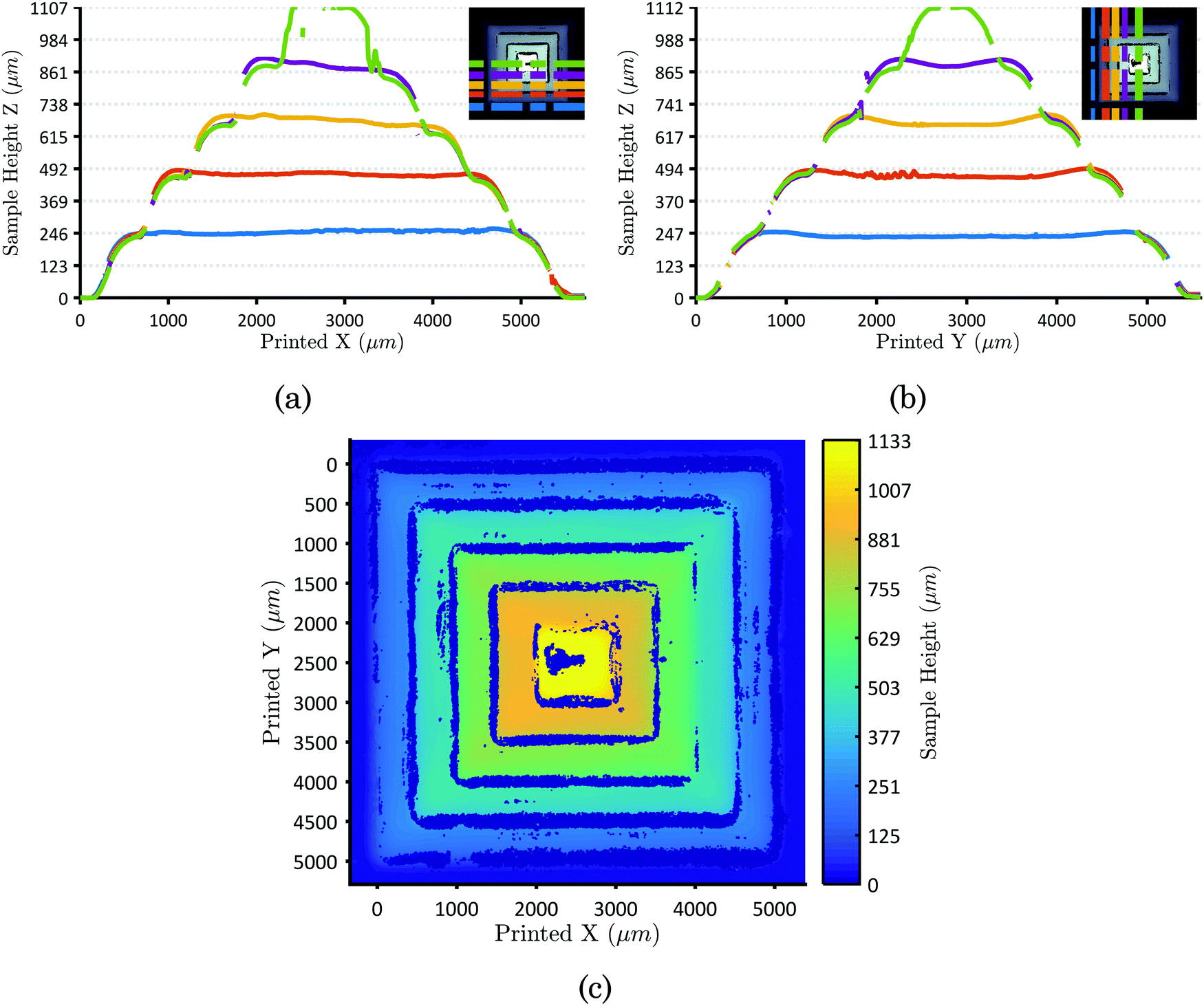 | ||
| Fig. 11 Profile analysis of the stepped ziggurat printed design conducted on the Alicona. Line scans are taken as an average in a number of lines and shown as (a) line scans immediately before a step in X, (b) line scans in Y, (c) area profile, with highlights where line scans were taken from. | ||
The profile of the printed ziggurat, moving in the X direction across the stepped regions, shows that the first two steps produce a highly uniform and level line, but with further layers an inclination appears. This sloping is likely related to the increased variation in the other direction, indicative of increasing time to cure.
Curing in printed PDMS
The Raman analysis was conducted on samples printed with the layer based printing method. This was done to determine if the FRIJP process is capable of mixing the PDMS system on the substrate during printing. The FTIR-ATR system was used to determine degree of cure after determining that there were no concentration gradients in the printed PDMS.The process of FRIJP relies heavily on the ability of the two components to mix in situ, as there is little mixing from the drop impact.40 Therefore, in the case of FRIJP PDMS the sole mechanism for mixing is the diffusion of the two components. The miscibility of the inks aids this diffusion, and in the case of PDMS no effects from improper mixing were observed, e.g. interfaces, liquid PDMS, gelling. Confocal Raman was conducted to study if, and how, the substrate temperature can affect the mixing in RIJP. The analysis had two objectives. First it aimed to determine the residual crosslink component across the sample. Second, it set out to determine whether the PDMS is a homogenous polymer or if there are compositional variations.
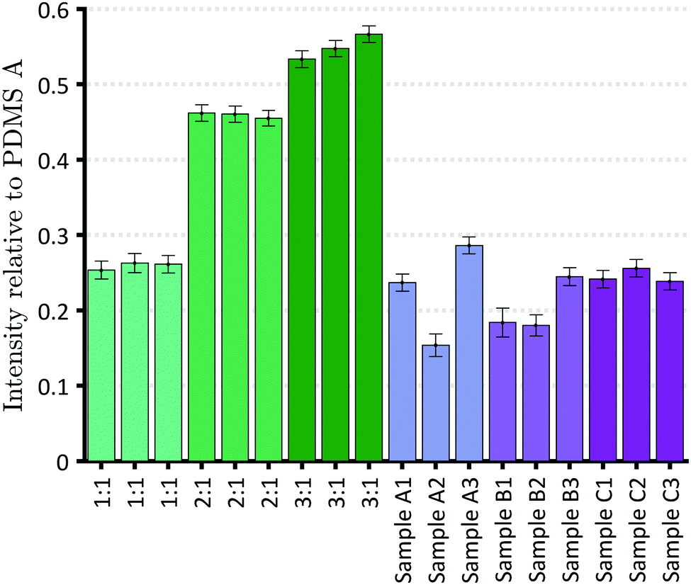
For the analysis the residual hydride concentration is compared to the initial concentration. As mixing and reaction occurs this hydride will decrease, depending on the formulation once correctly mixed, there may or may not be excess hydride by design. To determine what the correct residual is, three calibration samples were also analysed with the Raman. The calibration samples were made following the manufacturers guide. In Fig. 12, the residual hydride component is compared to the initial concentration of Si–H in the PDMS A component (The representative spectra as shown in Supplementary 1, ESI†). This demonstrated that although there wasn’t exact correspondence, the printed samples tended to show similar PDMS A intensities to those seen in 1:1 cast samples, suggesting that printing results in material similar to that produced by more traditional manufacturing methods.
 | ||
| Fig. 12 Quantified residual crosslink component in each printed sample in relation to uncured part A also included are cast samples created at 1:1 2:1 3:1 A:B ratio, data is shown as mean ± standard deviation (XY: n = 75, Z: n = 50). Representative Raman spectra for the PDMS is shown in Supplementary 1 (ESI†). | ||
An important consideration of the FRIJP process is that due to transport in the film it is possible for the mixing ratio across the sample to change. Confocal Raman was used to determine if the ratio between A and B is constant throughout the printed sample. There was no evidence for spatial dependency in any of the samples printed (with the exception of the 40 °C X direction scan). In the case of samples prepared at the lower temperatures, scanned in the X direction, there is significance in the residual Si–H and location on the print. This residual concentration in the low temperature sample is likely related to the domed profile also observed. It was found that there is no evidence for depth dependent concentration, which has been found in AM inkjet printed components cured with UV radiation.41 This demonstration of mixing & reacting in situ suggests that it is possible to produce homogenously crosslinked PDMS samples. However, care must be taken that the individual components are deposited in the correct ratio and that limited redistribution of ink occurs before curing.
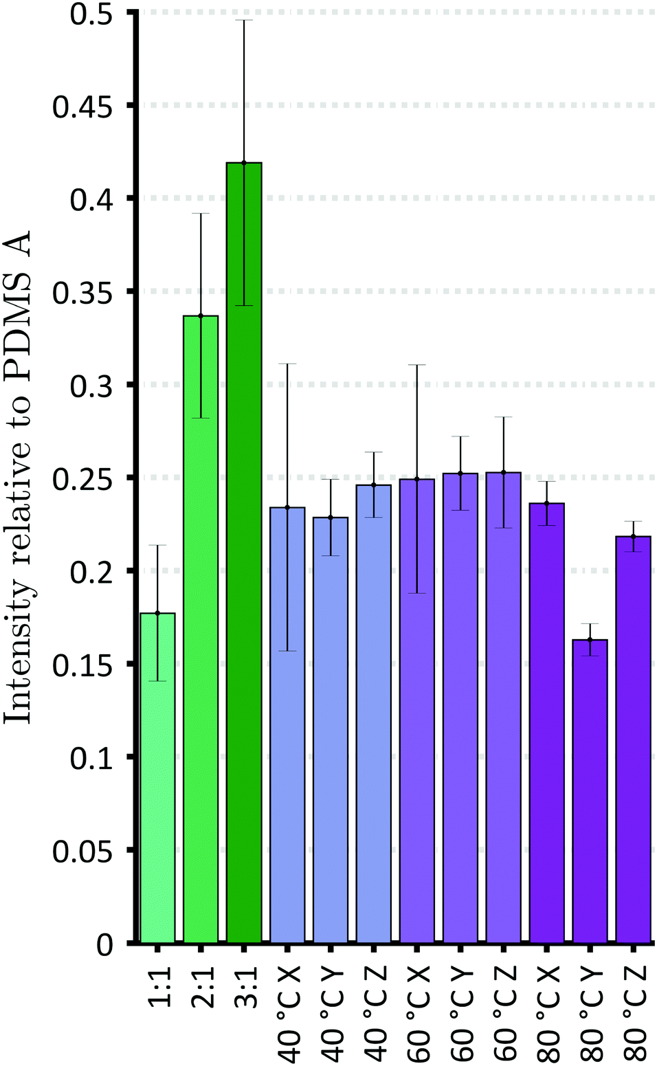
A further analysis was conducted on the samples printed using the second, line based, printing strategy. This printing strategy was also conducted with the corrected droplet ratios. The results of this analysis are shown in Fig. 13, they show that residual Si–H intensity in the printed samples corresponds to the 1:1 cast calibration. This shows that in all cases the printed samples were the same, or better, than the cast ones.
 | ||
| Fig. 13 Residual cross link component Si–H in the calibration and printed samples collected with FTIR-ATR. The bond at 912 cm−1 was used to determine the residual. The errors are from the curve fitting GOF of both the calibration and residual combined. Three sets of samples were taken from three separate prints. | ||
Conclusions
In this work the Reactive Inkjet Printing of Polydimethylsiloxane has been demonstrated. For the first-time multiple component, reactive jetting has been used to produce PDMS structures with shape definition in a crosslinked polymer network. A stable FRIJP ink was developed from a two-part silicone system. The viscosity of each component was such that a 60 wt% loading of polymer was achievable whilst maintain a printable ink.In FRIJP, as the reaction is separated into two inks, the time to cure not only includes the reaction, but also the time for deposition and mixing. To increase the control of the profile each one of these steps had to be shortened. The major concern was the time to mixing, which was dependent on the printed geometry, which was around 2 minutes (for 4 mm square sample) in the layer based approach. To reduce this both inks were printed in a single pass, the time to mixing was then independent of printed geometry and only dependent on head printing speed. The time to deposition was calculated to around 0.3 s. The reviewed literature stated no convective mixing occurred, leaving only diffusion based mixing for the PDMS system. The only method to increase this was then through substrate heating to elevate the liquid temperature.
Through the use of substrate heating it was found that the lowest degree of profile variation was found in the 80 °C print. This substrate heating also had an observable effect on the curing, with decreased residual Si–H components observed through Raman. When the line scan strategy was employed, to reduce the mixing time, substrate heating was maintained. The reduction on time to mixing had a direct effect on the printed profile, with the line scans showing much greater layer uniformity than the layer strategy. The sample curing was also improved with the change of strategy, where the samples showed residual Si–H component comparable to the conventionally manufactured 1:1 references.
The result of these improvements is a highly cross-linked PDMS network directly printed onto a glass substrate which was modified to increase the feature resolution. The printed geometry had an acceptable topology for a FRIJP part. A complex structure has been demonstrated, showing the capabilities of the FRIJP process to produce a single material sample without the aid of support. As it has been shown that PDMS samples can be produced through FRIJP the possibility to replace traditional casting techniques exists.
Conflicts of interest
There are no conflicts to declare.Acknowledgements
This work was supported by the Engineering and Physical Sciences Research Council [grant number EP/1033335/2], EPSRC Centre for Innovative Manufacturing in Additive Manufacturing. The authors are grateful to Dr Andrew Davies for technical assistance and to the Nanoscale and Microscale Research Centre (NMRC) for providing access to Raman microscopy facilities.References
- J.-P. Kruth, M. C. Leu and T. Nakagawa, CIRP Ann., 1998, 47, 525–540 CrossRef.
- A. Aremu, I. Ashcroft, R. Wildman, R. Hague, C. Tuck and D. Brackett, Proc. Inst. Mech. Eng., Part B, 2013, 227, 794–807 CrossRef.
- W. E. King, A. T. Anderson, R. M. Ferencz, N. E. Hodge, C. Kamath, S. A. Khairallah and A. M. Rubenchik, Appl. Phys. Rev., 2015, 2, 41304 Search PubMed.
- M. E. Hoque, Y. L. Chuan and I. Pashby, Biopolymers, 2011, 97, 83–93 CrossRef PubMed.
- N. Hopkinson, R. Hague and P. Dickens, Rapid Manufacturing: An Industrial Revolution for the Digital Age, Wiley, USA, 2005 Search PubMed.
- I. Gibson, D. W. Rosen and B. Stucker, Additive Manufacturing Technologies, Springer US, Boston, MA, 2010 Search PubMed.
- B. Derby, Annu. Rev. Mater. Res., 2010, 40, 395–414 CrossRef CAS.
- D. H. A. T. Gunasekera, S. Kuek, D. Hasanaj, Y. He, C. Tuck, A. Croft and R. D. Wildman, Faraday Discuss., 2016, 190, 509–523 RSC.
- B. J. deGans, P. C. Duineveld and U. S. Schubert, Adv. Mater., 2004, 16, 203–213 CrossRef.
- T. T. Nge, M. Nogi and K. Suganuma, J. Mater. Chem. C, 2013, 1, 5235 RSC.
- L. R. Hart, S. Li, C. Sturgess, R. Wildman, J. R. Jones and W. Hayes, ACS Appl. Mater. Interfaces, 2016, 8, 3115–3122 CAS.
- F. Zhang, C. Tuck, R. Hague, Y. He, E. Saleh, Y. Li, C. Sturgess and R. Wildman, J. Appl. Polym. Sci., 2016, 133, 43361 Search PubMed.
- Y. He, R. D. Wildman, C. J. Tuck, S. D. R. Christie and S. Edmondson, Sci. Rep., 2016, 6, 20852 CrossRef CAS PubMed.
- E. M. Hamad, S. E. R. Bilatto, N. Y. Adly, D. S. Correa, B. Wolfrum, M. J. Schöning, A. Offenhäusser and A. Yakushenko, Lab Chip, 2016, 16, 70–74 RSC.
- E. Carrilho, A. W. Martinez and G. M. Whitesides, Anal. Chem., 2009, 81, 7091–7095 CrossRef CAS PubMed.
- P. J. Smith and A. Morrin, J. Mater. Chem., 2012, 22, 10965 RSC.
- T. Sekitani, Y. Noguchi, U. Zschieschang, H. Klauk and T. Someya, Proc. Natl. Acad. Sci. U. S. A., 2008, 105, 4976–4980 CrossRef CAS PubMed.
- P. Kröber, J. T. Delaney, J. Perelaer and U. S. Schubert, J. Mater. Chem., 2009, 19, 5234 RSC.
- S. Fathi, Fundamental Investigation on Inkjet Printing of Reactive Nylon Materials, PhD thesis, https://dspace.lboro.ac.uk/2134/7832 Search PubMed.
- K. Kim, S. Il Ahn and K. C. Choi, Curr. Appl. Phys., 2013, 13, 1870–1873 CrossRef.
- B. H. Jo, L. M. Van Lerberghe, K. M. Motsegood and D. J. Beebe, J. Microelectromech. Syst., 2000, 9, 76–81 CrossRef CAS.
- S. Camou, H. Fujita and T. Fujii, Lab Chip, 2003, 3, 40–45 RSC.
- Z. Cai, W. Qiu, G. Shao and W. Wang, Sens. Actuators, A, 2013, 204, 44–47 CrossRef CAS.
- D. A. Chang-yen, R. K. Eich and B. K. Gale, J. Lightwave Technol., 2005, 23, 2088–2093 CrossRef CAS.
- S. Kopetz, D. Cai, E. Rabe and A. Neyer, Int. J. Electron. Commun., 2007, 61, 163–167 CrossRef.
- J. Sun, J. Jiang, B. Bao, S. Wang, M. He, X. Zhang and Y. Song, Materials (Basel)., 2016, 9, 253 Search PubMed.
- M. N. Kirikova, E. V. Agina, A. A. Bessonov, A. S. Sizov, O. V. Borshchev, A. A. Trul, A. M. Muzafarov and S. A. Ponomarenko, J. Mater. Chem. C, 2016, 4, 2211–2218 RSC.
- T. J. Hinton, A. Hudson, K. Pusch, A. Lee and A. W. Feinberg, ACS Biomater. Sci. Eng., 2016, 2, 1781–1786 CrossRef CAS PubMed.
- D. B. Kolesky, R. L. Truby, A. S. Gladman, T. A. Busbee, K. A. Homan and J. A. Lewis, Adv. Mater., 2014, 3124–3130 CrossRef CAS PubMed.
- Y. Sung, J. Jeang, C. Lee and W. Shih, J. Biomed. Opt., 2015, 20, 47005 CrossRef PubMed.
- Jettable Fluid Formulations Guidelines, 1.
- N. Reis, C. Ainsley and B. Derby, J. Appl. Phys., 2005, 97, 94903 CrossRef.
- S. A. Mumford and J. W. C. Phillips, J. Chem. Soc., 1950, 75–84 RSC.
- D. Cai, A. Neyer, R. Kuckuk and H. M. Heise, J. Mol. Struct., 2010, 976, 274–281 CrossRef CAS.
- S. Gasparin, H. N. Hansen and G. Tosello, in 13th International Conference on Metrology and Properties of Engineering Surfaces, April, 2011.
- S. H. Lee and Y. J. Cho, J. Electr. Eng. Technol., 2012, 7, 91–96 CrossRef.
- J. Stringer and B. Derby, Langmuir, 2010, 26, 10365–10372 CrossRef CAS PubMed.
- S. Vafaei, C. Tuck, I. Ashcroft and R. Wildman, Chem. Eng. Res. Des., 2016, 109, 414–420 CrossRef CAS.
- A. B. Thompson, C. R. Tipton, A. Juel, A. L. Hazel and M. Dowling, J. Fluid Mech., 2014, 761, 261–281 CrossRef CAS.
- J. R. Castrejón-Pita, K. J. Kubiak, a. a. Castrejón-Pita, M. C. T. Wilson and I. M. Hutchings, Phys. Rev. E: Stat., Nonlinear, Soft Matter Phys., 2013, 88, 23023 CrossRef PubMed.
- X. Chen, I. A. Ashcroft, R. D. Wildman and C. J. Tuck, Proc. R. Soc. A, 2015, 471, 20150477 CrossRef CAS PubMed.
Footnote |
| † Electronic supplementary information (ESI) available. See DOI: 10.1039/c7tc02412f |
| This journal is © The Royal Society of Chemistry 2017 |