
 Open Access Article
 This Open Access Article is licensed under a Creative Commons Attribution-Non Commercial 3.0 Unported Licence
Transport in polymer-supported chemically-doped CVD graphene†
Moon H.
Kang‡
 *a,
Guangyu
Qiu
b,
Bingan
Chen
c,
Alex
Jouvray
c,
Kenneth B. K.
Teo
c,
Cinzia
Cepek
d,
Lawrence
Wu
b,
Jongmin
Kim
a,
William I.
Milne
ae and
Matthew T.
Cole
*f
*a,
Guangyu
Qiu
b,
Bingan
Chen
c,
Alex
Jouvray
c,
Kenneth B. K.
Teo
c,
Cinzia
Cepek
d,
Lawrence
Wu
b,
Jongmin
Kim
a,
William I.
Milne
ae and
Matthew T.
Cole
*f
aElectrical Engineering Division, Department of Engineering, University of Cambridge, 9 JJ Thomson Avenue, Cambridge, CB3 0FA, UK. E-mail: mhk29@cam.ac.uk
bCity University of Hong Kong, Tat Chee Avenue, Kowloon, Hong Kong, Republic of China
cAixron Ltd, Buckingway Business Park, Swavesey, CB24 4FQ, UK
dIstituto Officina dei Materiali-CNR, Laboratorio TASC, Trieste I-34149, Italy
eQuantum Nanoelectronics Research Centre, Tokyo Institute of Technology, 2-12-1 O-okayama, Tokyo, 152-8552, Japan
fDepartment of Electronic and Electrical Engineering, University of Bath, Bath, BA2 7AY, UK. E-mail: m.t.cole@bath.ac.uk
First published on 7th September 2017
Abstract
In this study we report on the electron transport in flexible-transparent polymer supported chemically doped chemical vapour deposited (CVD) graphene. We investigate the modified carrier transport following doping with various metal chlorides. An increase in the work function was noted for AuCl3-, FeCl3-, IrCl3-, and RhCl3-doping, whilst only SnCl2 doping showed a reduced work function. We attribute this to dopant-mediated charge transfer resulting in the formation of neutral atomic species. The neutral and near-neutral atomic populations produced metallic aggregates, with this agglomeration level critically dependent on the cohesive energy of the metallic component in each dopant. Micron-scale spatial conductivity mapping highlighted the spatially uniform low resistance of AuCl3-doped graphene. Local conductivity enhancements at grain boundaries and lattice defects within the as-synthesised polycrystalline graphene suggested that the dopant molecules tend to reside at lattice imperfections. Temperature dependent transport studies indicated that the shifted work function improved electrical conductivity due to the increase of barrier transparency between grain boundaries. Variable Range Hopping (VRH) dominated at temperatures <140 K in undoped graphene, whereas combined Nearest Neighbour Hopping (NNH) and diffusive transport appears to play a major role throughout the transport in all doped samples. The findings herein reveal that the underlying extended transport mechanisms associated with chemically doped CVD graphene transferred to polymer supports contrast with the highly localised transport in undoped graphene.
Introduction
Graphene, a two-dimensional lattice of hexagonally arrayed carbon atoms, has attracted much attention for various commercial applications given its diverse, and largely unique set of electrical, optical and mechanical properties.1 Though promising and industrially attractive, the high sheet resistance of chemical vapour deposited (CVD) graphene necessitates the development of improved methodologies of enhancing the nascent materials’ electrical conductivity, without which it will remain challenging to integrate into various large area flexible electronics technologies, such as organic light emitting diodes (OLED),2–4 capacitive touch screens5,6 and photovoltaic cells.7–9 Such applications require areal uniformity, mechanical stability, and strong and long-lasting adhesion between the graphene and substrate upon flexing. There is also a pressing need for a means of work function tuning and this, as a result, has been studied for some time. For large area electronics (typically >10 cm × 10 cm), simultaneous conductance uniformity at the macro and micro scales, is critical. Chemical vapour deposition is one of the few industrially viable methods that allows for such large area, uniform synthesis, along with ambient pressure roll-to-roll processing, of truly monolayer materials of quality that is now comparable to the best exfoliated samples.10,11 CVD is gaining ever increasing traction. Coupled to its decreasing cost, CVD is proving to be one of the most attractive approaches for the high yield synthesis of large area graphene materials.10To be of use in most electronic applications, the as-synthesised nascent CVD graphene must be transferred to arbitrary insulating substrates from the opaque and conductive catalyst upon which it is grown. Various transfer methods have been developed to maintain the quality of the as-grown graphene during transfer.12–14 In our earlier work we reported an approach to transfer graphene onto flexible substrates with one of the highest adhesion potentials between the graphene and substrate reported to date.15,16 Though such work demonstrated the mechanical robustness of these polymer-supported layered systems, it remains nonetheless critical to elucidate the underlying electron transport in such transferred two dimensional materials, particularly in order to guide us towards further conductivity improvements. The conductivity of pristine monolayer CVD graphene is, at present, too low to replace incumbent transparent conducting oxide electrodes.17,18 In pristine graphene, the density of states at, or near to, the Dirac point remains low, dramatically reducing the conductivity. As a result, various doping strategies have been developed as a critical means of increasing conductivity.19–22 Spray coating of silver nanowires has been shown to increase the conductivity of the graphene basal plane by ∼20 times with only a 4.3% decrease in optical transparency.23 Doping by plasma exposure24 has been shown to accurately control both the work function and electrical conductivity; 10 mTorr Cl2 plasma at 2 W RF power led to a +0.6 eV work function shift and two-fold increase in conductivity. However, in defective samples, such plasma readily exacerbates, and even nucleates lattice defects and, given the often elevated process temperatures used, this remains a challenging approach for many common polymer substrates. To avoid many of these issues, herein, we report on a room temperature chemical doping strategy based on the use of various metal chlorides in a facile chemi douche process. Chemical doping has been shown to decrease the sheet resistance (RS) of graphene from ∼2000 Ω sq.−1 to ∼90 Ω sq.−1 without significantly compromising the optical transparency (from ∼97% to ∼80%).25–27
Metal chlorides have been considered as a highly efficient dopants for a wide variety of carbon-based conducting materials.22,28–30 The charge transfer rate depends critically on the reaction potential of the selected dopant in relation to the native carbon. The metal chloride chosen for this study where selected due to the high charge transfer propensity and commensurate high reaction potential. In our previous work31 we reported on the conductivity and transparency of such systems before and after metal chloride doping, with our findings suggesting that molecular ad/desorption is one of the primary factors contributing to the observed time-dependent shifts in the doping level and, hence, conductivity. In the present report, we extend this earlier work by investigating the detailed temperature dependent electron transport within these doped graphene materials, focussing on the shift in work function and the associated impacts of dopant agglomerate formation.
Experiment
Monolayer graphene was grown by CVD, as reported in ref. 15. The polycrystalline graphene was transferred from the Cu foil catalyst to polyethylene terephthalate (PET) using an Ultraviolet Adhesive (UVA) procedure, as similarly detailed elsewhere.16 After transfer, the graphene-on-PET was chemically doped with one of five chloride compounds; AuCl3, FeCl3, SnCl2, IrCl3, or RhCl3. Dopant solutions were spin-cast onto the transferred graphene samples at 2000 rpm for 1 min after a 30 s spread at 500 rpm. The effects on the conductivity as a function of dopant concentration have been reported elsewhere.31 Optical images of typical transferred and doped graphene on PET are shown in the inset of Fig. 1(b) and (c).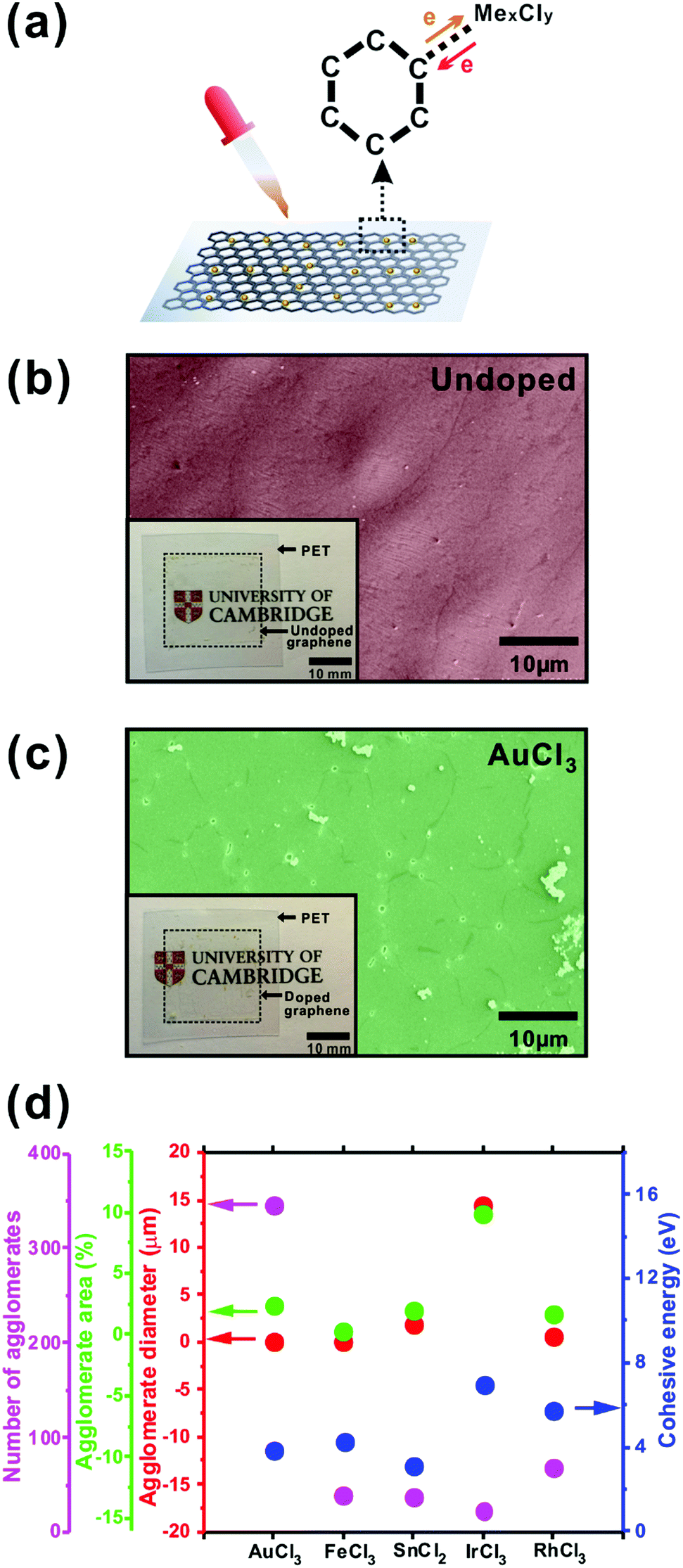 | ||
| Fig. 1 (a) Doping scheme. SEM micrographs and optical photographs (insets) of (b) undoped and (c) AuCl3-doped graphene, and (d) comparison of the metal constituent cohesive energy with the number of agglomerates, agglomerate diameter and total agglomerate-covered area. | ||
As described in Fig. 1(a), the metal chloride (MexCly) is physically adsorbed, mediating spontaneous charge transfer across well-defined energy levels at the graphene–metal ion interface. In the present system, such an interaction can be expressed as (1)–(3):31,32
| Graphene + 2MeCl3 → Graphene + MeCl2− + MeCl4− | (1) |
| 3MeCl2− → 2Me0 + MeCl4− + 2Cl− | (2) |
| MeCl4− + Graphene → Graphene+ + Me0 + 4Cl− | (3) |
| Sn(OH)Cl + HCl + Graphene + O → SnO2 + 2HCl + Graphene− | (4) |
As seen in Fig. 1(c), upon doping, particles 5–15 μm in diameter form. No such substantial particles were noted prior to doping (Fig. 1(b)). EDX suggests that these particles are very likely dopant agglomerates which form from the incomplete dissolution of the powdered dopant, or as a result of charge transfer induced agglomeration. As described above, the metal chlorides transfer surplus charge to the graphene basal plane leaving charge-neutral metal atoms (Me0) or, in the somewhat anomalous case of SnCl2, SnO2. Such neutral metallic constituents tend to aggregate under aqueous conditions and are subsequently fixed upon drying, with their formation dictated by the magnitude of the metal constituents cohesive energy. The total areal coverage and number of agglomerate particles are shown in Fig. 1(d). AuCl3-doped graphene shows the largest number of agglomerates, however the size of these agglomerates is smaller by 7.5%/99.2% for FeCl3/IrCl3, respectively. Though the number of agglomerates of the IrCl3-doped was smaller than that of the AuCl3-doped, the average diameter of the agglomerates was significantly larger (14.4 μm) than that of the AuCl3 (0.1 μm), with the total agglomerate area being the largest for IrCl3-doped samples (9.91%) as a result.
Cohesive energy (CE) is defined as the energy needed to sub-divide a metal into isolated atoms.34 Metals with a low CE are readily chemically separated, whilst those of comparatively high CE produce larger particles. The calculated CE of the considered metallic constituents is reported in Fig. 1(d).35 There appears a notable correlation between the magnitude of the CE and the degree of agglomeration of the metallic species. CE seems to play a contributing role in governing agglomerate formation and thus, concurrently, the resulting optical transparency and sheet resistance. The large CE of Ir (6.94 eV) indicates that Ir has perhaps the greatest likelihood of inducing significant agglomeration, consistent with our experimental findings. Across all the dopants, SnCl2 was somewhat atypical. The CESn = 3.14 eV, which was smaller than that of Au (3.81 eV) and Fe (4.28 eV), however the average diameter of the agglomerates (1.95 μm) was larger than found in both the Au (0.11 μm) and Fe (0.12 μm). The agglomerate covered area of Sn (1.96%) was smaller than that of Au (2.39%), but larger than that of Fe (0.31%), which is largely inconsistent with cohesion-driven agglomeration. Nevertheless, this likely relates to the disparate doping mechanism associated with SnCl2 compared with the other considered MexCly. SnO2 remains after SnCl2 doping. No Sn neutral species were formed which likely gives rise to the poor correlation between the generation of SnO2 and CESn.
To further investigate the areal uniformity of the chemical doping, sub-micro-scale scanning spreading resistance microscopy (SSRM)36,37 was performed using a conductive cantilever (Applied NanoStructures, Inc., SICONA) atomic force microscope (AFM, Veeco Instruments Inc., Dimension icons). With a spatial resolution of Δx,y ∼ 11.7 nm, 3 μm × 3 μm areas were scanned with the sample edges electrically grounded in all cases. Probing the relationship between surface roughness and spreading resistance upon doping allows for immediate comparisons of the nanoscale and macroscale resistance distributions, the latter of which was measured via contact four-point probe mapping. For the undoped graphene, SSRM and surface morphology data appear near coincident (Fig. 2(a) and (c)); valleys of comparable vertical dimensions appear less likely to effectively attach to the graphene during the transfer process with such substrate irregularities prohibiting proximal contact between the substrate and the graphene.38 The graphene in these features is not completely transferred, but rather partially lost; consequently the valleys tend to have higher resistance than the surrounding ridges. These substrate effects have been shown elsewhere to be minimised through the use of suspended graphene.39 Contrasting results were found in some areas of the AuCl3 doped graphene (black and red arrows, Fig. 2(b) and (d)). Studies elsewhere suggest that such features manifests as highly-resistive line defects. However, in the present case the narrow lines showed a surprising reduction in resistance relative to the nascent surrounding graphene. We find that dopant molecules, which do not noticeably augment the feature topography, adhere to these defect sites which include; abrupt changes in the surface morphology such as folds, grain boundaries, cracks and other lattice non-idealities, with such preferential adsorption reducing the feature resistance to values lower than the surrounding graphene. This grain healing is notable upon MexCly doping. Chang et al. argued that adatoms on graphene have a tendency to dwell on atomic steps or boundaries.40 Such molecules are largely beyond the detectable limit of the present AFM morphology study, though nonetheless contribute to a measurable change in the conduction. The dopant distribution is inhomogeneous, with a tendency for accumulation at edges, steps, grain boundaries, or other defects. The conductive edge and grain boundaries may possibly contribute to the charge transport by functioning as a percolation network of sub-nanometre wires, and is the focus of further study.
 | ||
| Fig. 2 Atomic Force Microscopic (AFM) maps of (a) undoped, (b) AuCl3-doped graphene. Scanning Spreading Resistance Microscopy (SSRM) maps of (c) undoped and (d) AuCl3-doped graphene. The black arrow in (b) and in (d) denotes a typical narrow valley and the corresponding low resistance of this feature, respectively. | ||
X-ray Photoemission Spectra (XPS) were acquired using a Mg source (1253 eV) with an energy resolution of 0.092 eV. To measure the change in work function following chemical doping, Ultraviolet Photoemission Spectra (UPS) were measured using a He I lamp (21.2 eV) with an energy resolution of 0.061 eV. For XPS and UPS measurement the as-grown graphene was transferred to polished molybdenum substrates as our earlier efforts indicated that the polymer substrates induced serious charging effects. As shown in Fig. 3(a), the work function of the doped graphene shifted by +0.23 eV (AuCl3), +0.32 eV (FeCl3), +0.11 eV (IrCl3), and +0.13 eV (RhCl3) from undoped graphene indicating p-doping compared to the undoped scenario, consistent with our Raman results (ESI,† Fig. S4), whereas SnCl2-doped graphene exhibited a similar work function to that of the undoped graphene, with only +0.06 eV shift.
 | ||
| Fig. 3 (a) Secondary UPS cut-off and XPS C1s peak for (b) undoped, (c) AuCl3-, (d) FeCl3-, (e) SnCl2-, (f) IrCl3-, and (g) RhCl3-doped graphene. (h) C–C sp2 peak position of the undoped and doped graphene. | ||
The Voigt-convolution fitted41 C1s peak of the undoped and the MexCly doped graphene are shown in Fig. 3(b)–(g). Two principle carbon bonding components; C–C sp2 at 284.6 eV and C–C sp3 at 285.8 eV are shown, alongside the oxygen containing functional groups (C–O(hydroxyl) and C![[double bond, length as m-dash]](https://www.rsc.org/images/entities/char_e001.gif) O(carboxyl) at 286.0 eV and 287 eV, respectively). In all doped cases, the sp3 peak does not significantly increase, indicating there is little defect generation induced by the doping procedure. Our Raman studies independently confirm this. Conversely, however; the C–O peak cross-section increases when doped with AuCl3 (286.4 eV), FeCl3 (287.2 eV), SnCl2 (287.6 eV), and IrCl3 (287.5 eV), even though there is no observable C–O peak in the vicinity of 286 eV in the undoped and RhCl3-doped graphene. The highest C–O peak occurred upon SnCl2-doping. It is possible that residual SnO2 products deleteriously bond to the graphene basal plane. Charge transfer can be examined via the C1s sp2 peak shift, attributable to an work function modification. As described in Fig. 3(h), following chemical doping, the undoped graphene peak (284.28 eV) shifted to lower values for AuCl3 (284.19 eV), FeCl3 (284.19 eV), IrCl3 (284.22 eV), and RhCl3 (284.11 eV) indicating p-doping, whilst it moved to higher binding energy in SnCl2-doped graphene (284.34 eV) indicating n-doped characteristics compared to the undoped graphene. There was no additional peak generated from the metal chloride–carbon bonding which is a significant benefit compared to doping mediated by substitutional42 or thin film deposition.43 Chemical doping of polymer supported graphene under the present framework appears to be a promising approach to increase the conductivity and therein afford a means of controlling work function without a severely affecting the atomic structure of the as-grown graphene.
O(carboxyl) at 286.0 eV and 287 eV, respectively). In all doped cases, the sp3 peak does not significantly increase, indicating there is little defect generation induced by the doping procedure. Our Raman studies independently confirm this. Conversely, however; the C–O peak cross-section increases when doped with AuCl3 (286.4 eV), FeCl3 (287.2 eV), SnCl2 (287.6 eV), and IrCl3 (287.5 eV), even though there is no observable C–O peak in the vicinity of 286 eV in the undoped and RhCl3-doped graphene. The highest C–O peak occurred upon SnCl2-doping. It is possible that residual SnO2 products deleteriously bond to the graphene basal plane. Charge transfer can be examined via the C1s sp2 peak shift, attributable to an work function modification. As described in Fig. 3(h), following chemical doping, the undoped graphene peak (284.28 eV) shifted to lower values for AuCl3 (284.19 eV), FeCl3 (284.19 eV), IrCl3 (284.22 eV), and RhCl3 (284.11 eV) indicating p-doping, whilst it moved to higher binding energy in SnCl2-doped graphene (284.34 eV) indicating n-doped characteristics compared to the undoped graphene. There was no additional peak generated from the metal chloride–carbon bonding which is a significant benefit compared to doping mediated by substitutional42 or thin film deposition.43 Chemical doping of polymer supported graphene under the present framework appears to be a promising approach to increase the conductivity and therein afford a means of controlling work function without a severely affecting the atomic structure of the as-grown graphene.
UPS and XPS collectively suggest that charge transfer underpins the present chemical doping framework. However, direct evidence on the amount of charge transfer can be gleaned by Hall measurements (Fig. 4). Van der Pauw geometries were fabricated and samples measured at room temperature under a 2 kG field.
 | ||
| Fig. 4 Transport in undoped and MexCly-doped graphene: (a) sheet resistance (RS), (b) carrier density, and (c) work function shift calculated with empirical carrier density values. | ||
The RS of the graphene decreased from 2148 Ω cm−2 (undoped graphene) to 1026 Ω cm−2 (AuCl3), 853 Ω cm−2 (FeCl3), 1521 Ω cm−2 (SnCl2), and 1109 Ω cm−2 (RhCl3). The RS reduction is consistent with our earlier macro-scale four-point probe measurements.31 Only IrCl3-doped graphene exhibited a higher RS (68 MΩ cm−2) than the undoped samples (Fig. 4(a)), which differs from other published works.22,28,29 This may be associated with the topological insulating behaviour of Ir on graphene44–46 though further investigations are ongoing to explore this.
The carrier density of undoped graphene was 2.0 × 1012 cm−2, which is comparable to published values (9.3 × 10¹¹–3.4 × 1012 cm−2),43,47–50 whereas the carrier density of the doped graphene increased by roughly an order of magnitude (8.5 × 1012 cm−2 (SnCl2)–2.8 × 1013 cm−2 (AuCl3)). Only IrCl3 doped graphene showed a lower carrier density (1.4 × 109 cm−2). The Hall carrier mobilities for undoped and doped graphene can be obtained by51
 | (5) |
Kelvin Probe Force Microscopy (KPFM, Bruker Co.) was used to independently corroborate the measured work function shifts upon chemical doping, as well as concurrently exploring any microscale spatial variation. The surface potential of graphene was scanned over 20 μm × 20 μm and the work function (φGraphene) extracted (Fig. 5(a) and (b)). Undoped graphene had a work function of 4.72 eV, which was slightly higher than previously reported (4.66 eV).56,57 This slight increase is likely due to unintentional doping of the graphene following interaction with ambient atmosphere.54,58,59 The work function of the SnCl2-doped graphene was shifted by −0.13 eV from the undoped graphene, whilst the remainder of the doped graphenes showed positive shifts in their work functions ranging from 0.07 to 0.31 eV. The areal distribution of the work function appears especially uniform with a standard deviation per unit area ranging from only 0.04 eV (RhCl3) to 0.21 eV (FeCl3).
 | ||
| Fig. 5 KPFM maps of (a) undoped and (b) AuCl3-doped graphene, (c) comparison of measured work function and published data,21,22,28,56 (d) an example plot of the charge transfer reaction of MexCly-doped CVD graphene and comparison of work function shift values measured by KPFM with (e) Gibb's free energy and (f) reduction potential. | ||
In Fig. 5(c) we compare the work function shift for all doped samples obtained by KPFM, UPS, Hall measurement and Density Function Theory (DFT). DFT calculations were performed using Material Studio 7.0 and DMol3, with calculations based on a 3 nm × 3 nm basal plane. The generalized gradient approximation with Perdew–Burke–Ernzerhof functional (GGA-PBE) was applied for the exchange–correlation function. The trend in the work function shift from the DFT models is in broad agreement with our KPFM results. However, FeCl3, SnCl2 and RhCl3 all showed a ∼0.3 eV higher work function compared to KPFM, UPS and Hall measurements. The difference is likely attributable to non-idealities associated with the graphene, its synthesis and doping; including, but not limited to, unintentional doping of the graphene upon exposure to ambient conditions and the catalyst etchant, in addition to the proximal substrate and UV adhesive. Nevertheless, the observed trends are consistent with our other empirical findings.
Achieving a high degree of charge transfer is central to increasing the doping level. This depends on two properties; the Gibb's free energy and the reduction potential of the dopants. The Gibb's free energy (ΔG) is defined as the thermodynamic potential used to calculate the maximum or reversible work that may be performed by a thermodynamic system at a constant temperature.60 Charge transfer is endothermic (ΔG < 0); it readily accelerates the reaction when ΔG is increasingly negative, as illustrated Fig. 5(d). The metal ions (Me3+) in the dopants are increasingly likely to achieve neutrality (Me0) with larger |ΔG| by positive charge transfer to the graphene, resulting in a larger work function shift. The Gibb's free energy values of the constituent metal atoms for each dopant are compared with the empirically assessed work function values (KPFM) in Fig. 5(e).61 A mirrored trend in the work function values in relation to ΔG is evident. A large work function shift is observed in AuCl3 (0.31 eV) and IrCl3-doped graphene (0.25 eV) with both having large, negative ΔG (AuCl3: −145.7 kJ mol−1 and IrCl3: −179.9 kJ mol−1).61
Another influential parameter in driving the rate and direction of charge transfer in the present 2D system is the reduction potential.11 As seen in Fig. 5(f), the work function of the doped graphene shows a similar trend to that of the reduction potential of the metallic ions. The reduction reaction mediates p-type doping in graphene, leaving bound Me0. If the reduction potential is high, the rate of charge transfer increases resulting in a large increase in the work function. For n-type doping from SnCl2, the reduction potential during oxidation by Sn2+ is −0.19 V61 indicating that it has a tendency to donate electrons to graphene, whilst the other dopants tend to accept electrons with the positive potentials (AuCl3: 1.00 V, FeCl3: 0.77 V, IrCl3: 1.16 V, and RhCl3: 0.76 V).61 We thus anticipate that the graphene doped with AuCl3, FeCl3, IrCl3 and RhCl3 show nominally p-type behaviour, whereas graphene doped with SnCl2 would exhibit nominally n-type behaviour, which our empirical findings corroborate.
Variable Range Hopping (VRH) has been widely implicated as a dominant transport mechanism in such 1D and 2D ensemble nanomaterials.62,63 VRH is conduction by phonon-assisted quantum tunnelling between disordered localised states near EF, where the resistance (R) can be expressed as a function of temperature, T as:63,64
 | (6) |
VRH has been considered elsewhere to explain transport in undoped graphene with Fermi level (EF) at the Dirac point.63 However, work function shift achieved by chemical doping means that EF can clearly be adjusted by chemical doping to provide otherwise different transport regimes, which needs another transport model rather than VRH. To investigate conduction in our doped graphene, the current–voltage (I–V) characteristics were measured as a function of temperature from 77 K to room temperature (297 K) using a Keithley 4200SCS SMU. Cr/Au (10/80 nm) contacts were thermally evaporated and defined via shadow masking of circular transmission lines (Fig. 6(a)). A range of channel lengths was considered (L = 50–1000 μm), granting us simultaneous empirical access to the contact resistance. The differential resistance, R = (dV/di)V=0 was calculated for all temperatures. Undoped graphene shows an exponentially decreasing resistivity with temperature, over the measured temperature range, but other doped graphene shows increasing resistivity as the temperature rose above ∼110 K, as shown in Fig. 6(c); an effect that is not well captured using standard VRH-like models.
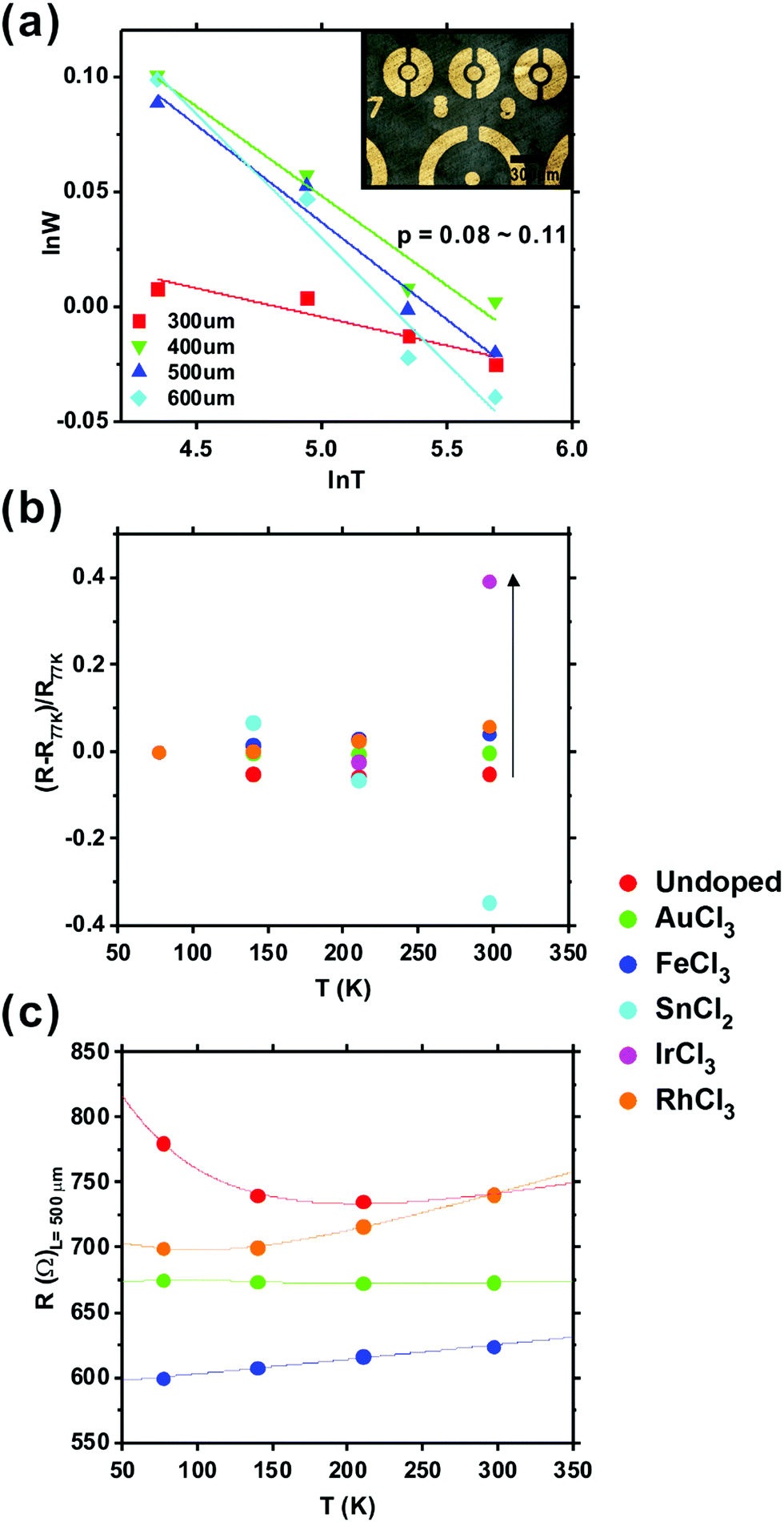 | ||
| Fig. 6 (a) A logarithmic derivative of the resistance calculated from the current–voltage (I–V) measured at various temperatures. Inset: Microscopic image of the Cr/Au circular transmission lines on the PET-supported CVD graphene. (b) The normalised resistance change with increasing temperature, and (c) example differential resistance calculated from the measured IV (L = 300 μm). | ||
The Zabrodskii's Reduced Activation Method (RAM)67 was used in order to determine the functional form of the T-dependent resistivity of VRH conduction. In this way the reduced activation energy (W = T−1∂![[thin space (1/6-em)]](https://www.rsc.org/images/entities/char_2009.gif) lnR/∂T−1) can be expressed as W(T) = A + x(T0/T)P by substituting the VRH model,
lnR/∂T−1) can be expressed as W(T) = A + x(T0/T)P by substituting the VRH model, 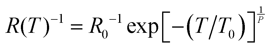 , we have
| lnW(T) ≈ ln(x(T0)P) − pln(T) | (7) |
Park et al. suggested a three-termed transport model for the temperature-dependent conduction in polycrystalline graphene.67 Adding Thermal Activation (TA) and Nearest Neighbour Hopping (NNH) to the existing VRH model, this composite modelled can be expressed as;67
 | (8) |
The conduction models outlined above focus on undoped graphene with EF at the Dirac point. There was no consideration for highly doped graphene with high carrier density showing metallic-like behaviour, as our empirical findings suggest. For such quasi-metallic behaviour, resistance may arise from electron–phonon scattering or electron-defect scattering, especially at elevated temperatures. We propose a model that explains the electrical conduction of doped graphene for the entirety of the temperature range considered. By introducing an increasing resistance term at high temperatures, associated with phonon coupling effects, we find a temperature dependency of the form;
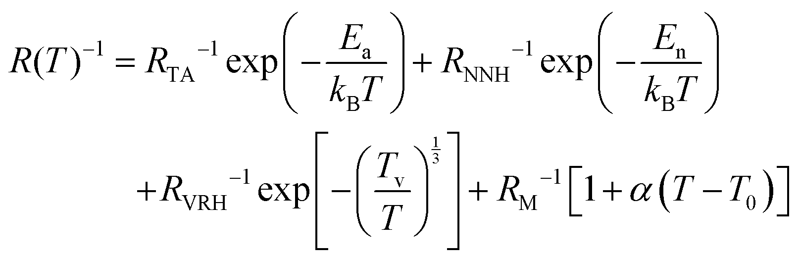 | (9) |
As described in Fig. 7, there are various potential barriers within the transferred graphene, though such said barriers are commonly low and easily overcome. Grain boundaries and defect states manifest other transport barriers which are increasingly opaque to transmission via hopping. For EF at the Dirac point in pristine, theoretically undoped graphene, the electron's become increasingly localised with high barriers at defects. It has been shown elsewhere that the grain boundary barrier height is inversely proportional to the doping level;71 the barrier height is lowered by the increasing doping level. Conversely, n-doping shifts EF to higher potentials therein reducing the effective barrier height; the wave function is extended and electrons move increasingly freely, as described in Fig. 7(b) and (c). Although the electron population may be localised between any given defect there remains a finite probability that tunnelling may occur via NNH. The barriers for holes are in the opposite direction upon p-doping and a similar transport mechanism can be applied.
 | ||
| Fig. 7 Transport in (a) pristine graphene, (b) n-doped, (c) p-doped graphene as a function of lattice and substrate induced potential barriers, such as grain boundaries. | ||
At high temperatures, charge carriers in the polymer-supported doped graphene appear to move with little barrier interference, enabling a low macroscale resistance, but a large number of extended carriers experience scattering from the substrate or other carriers. Upon doping, the possibility of carrier scattering is increased due to the increased number of carriers. VRH is dominant in pristine graphene, whilst doped graphene lies on the border between NNH and diffusive transport. Practically, measuring the T-dependent R of our undoped graphene we note a combination of VRH and NNH. The findings clarify that the electron transport of graphene can be extended rather than localised by chemical doping even at low temperatures, whilst scattering at high temperatures limits the absolute reduction in resistance. The elucidated transport mechanism is crucial for the control of work function and resistance of graphene by chemical doping, which underpins future graphene-based transparent flexible electronics devices.
Conclusion
Here we suggest a possible chemical doping scheme to augment charge transport in chemically-vapour deposited (CVD) graphene transferred to optically transparent and mechanically flexible polymer substrates. By conducting broad metrology studies, charge transport was studied before and after metal chloride doping with AuCl3, FeCl3, SnCl2, IrCl3 and RhCl3. Efficient charge transfer mediated by our doping scheme allows for accurate concurrent control over the resistance (3.5 kΩ to 0.93 Ω) and work function (−0.13 eV (SnCl2) ∼ 0.31 eV (AuCl3)). The agglomerates observed on graphene are generated from the neutral atoms whose propensity towards aggregation is principally dictated by their specific cohesive energy. SSRM mapping highlighted that dopant species tended to accrue at atomic facets and boundaries resulting in dominant NNH and diffusive transport which we independently verified through transport studies. Charge transport was investigated at various temperatures with Mott 2D VRH and NNH dominant in undoped graphene whilst NNH and diffusive transport were shown to play a major role in the doped graphenes with such contact interface nano-engineering which makes properly aligned work functions and improving electrical conductance between two inhomogeneous material and the demonstrable control over the work function by chemical doping. The presented work function tuning suggests that graphene is an ideal material for applications where work function optimisation is functionally essential in a new generation of transparent flexible electronics – such as in electron field emission applications, carrier injection layers in OLED and solar cells – as well as highlighting one possible means of advanced contact interface engineering.Conflicts of interest
There are no conflicts to declare.Acknowledgements
MTC thanks the Oppenheimer Research Trust and the University of Bath for generous financial support.References
- K. S. Novoselov, A. K. Geim, S. V. Morozov, D. Jiang, Y. Zhang, S. V. Dubonos, I. V. Grigorieva and A. A. Firsov, Electric field effect in atomically thin carbon films, Science, 2004, 306(5696), 666–669 CrossRef CAS PubMed.
- T.-H. Han, Y. Lee, M.-R. Choi, S.-H. Woo and S.-H. Bae, Extremely efficient flexible organic light-emitting diodes with modified graphene anode, Nat. Photonics, 2012, 6(2), 105–110 CrossRef CAS.
- J. Wu, M. Agrawal, H. A. Becerril, Z. Bao and Z. Liu, Organic light-emitting diodes on solution-processed graphene transparent electrodes, ACS Nano, 2010, 4(1), 43–48 CrossRef CAS PubMed.
- S. Bae, H. Kim, Y. Lee, X. F. Xu, J.-S. Park, Y. Zheng, J. Balakrishnan, T. Lei, H. Ri Kim, Y. I. Song, Y.-J. Kim, K. S. Kim, B. Ozyilmaz, J.-H. Ahn, B. H. Hong and S. Iijima, Roll-to-roll production of 30-inch graphene films for transparent electrodes, Nat. Nanotechnol., 2010, 5(8), 574–578 CrossRef CAS PubMed.
- J. Lee, M. T. Cole, J. C. S. Lai and A. Nathan, An Analysis of Electrode Patterns in Capacitive Touch Screen Panels, J. Disp. Technol., 2014, 10(5), 362–366 CrossRef.
- K. Jaeho, I. Masatou, K. Yoshinori, T. Kazuo, H. Masataka and I. Sumio, Low-temperature synthesis of large-area graphene-based transparent conductive films using surface wave plasma chemical vapor deposition, Appl. Phys. Lett., 2011, 98(9), 091502 CrossRef.
- P. Lin, W. C. H. Choy, D. Zhang, F. Xie, J. Xin and C. W. Leung, Semitransparent organic solar cells with hybrid monolayer graphene/metal grid as top electrodes, Appl. Phys. Lett., 2013, 102(11), 113303 CrossRef.
- H. Park, P. R. Brown, V. Bulovic and J. Kong, Graphene as transparent conducting electrodes in organic photovoltaics: studies in graphene morphology, hole transporting layers, and counter electrodes, Nano Lett., 2012, 12(1), 133–140 CrossRef CAS PubMed.
- Y. Un Jung, S.-I. Na, H.-K. Kim and S. Jun Kang, Organic photovoltaic devices with low resistance multilayer graphene transparent electrodes, J. Vac. Sci. Technol., A, 2012, 30(5), 050604 Search PubMed.
- K. S. Kim, Y. Zhao, H. Jang, S. Y. Lee, J. M. Kim, K. S. Kim, J. H. Ahn, P. Kim, J. Y. Choi and B. H. Hong, Large-scale pattern growth of graphene films for stretchable transparent electrodes, Nature, 2009, 457(7230), 706–710 CrossRef CAS PubMed.
- X. Li, W. Cai, J. An, S. Kim, J. Nah, D. Yang, R. Piner, A. Velamakanni, I. Jung, E. Tutuc, S. K. Banerjee, L. Colombo and R. S. Ruoff, Large-area synthesis of high-quality and uniform graphene films on copper foils, Science, 2009, 324(5932), 1312–1314 CrossRef CAS PubMed.
- J. Kang, D. Shin, S. Bae and B. H. Hong, Graphene transfer: key for applications, Nanoscale, 2012, 4(18), 5527–5537 RSC.
- C. s. J. L. de la Rosa, J. Sun, N. Lindvall, M. T. Cole, Y. Nam, M. Löffler, E. Olsson, K. B. K. Teo and A. Yurgens, Frame assisted H2O electrolysis induced H2 bubbling transfer of large area graphene grown by chemical vapor deposition on Cu, Appl. Phys. Lett., 2013, 102(2), 022101 CrossRef.
- N. Liu, Z. Pan, L. Fu, C. Zhang, B. Dai and Z. Liu, The origin of wrinkles on transferred graphene, Nano Res., 2011, 4(10), 996–1004 CrossRef CAS.
- M. H. Kang, W. I. Milne and M. T. Cole, Doping stability and opto-electronic performance of chemical vapour deposited graphene on transparent flexible substrates, IET Circuits, Devices Syst., 2014, 1, 1–7 Search PubMed.
- M. H. Kang, L. O. Prieto López, B. Chen, K. Teo, J. A. Williams, W. I. Milne and M. T. Cole, Mechanical Robustness of Graphene on Flexible Transparent Substrates, ACS Appl. Mater. Interfaces, 2016, 8(34), 22506–22515 CAS.
- K. S. Novoselov, A. K. Geim, S. V. Morozov, D. Jiang, M. I. Katsnelson, I. V. Grigorieva, S. V. Dubonos and A. A. Firsov, Two-dimensional gas of massless Dirac fermions in graphene, Nature, 2005, 438(7065), 197–200 CrossRef CAS PubMed.
- A. K. Geim, Graphene: Status and Prospects, Science, 2009, 324(5934), 1530–1534 CrossRef CAS PubMed.
- S. Yi, F. Wenjing, L. H. Allen and K. Jing, Iron(III) Chloride doping of CVD graphene, Nanotechnology, 2014, 25(39), 395701 CrossRef PubMed.
- S. Oh, B.-J. Kim and J. Kim, Layer-by-layer AuCl3 doping of stacked graphene films, Phys. Status Solidi RRL, 2014, 8(5), 441–444 CrossRef CAS.
- K. C. Kwon, B. J. Kim, J.-L. Lee and S. Y. Kim, Effect of anions in Au complexes on doping and degradation of graphene, J. Mater. Chem. C, 2013, 1(13), 2463–2469 RSC.
- K. C. Kwon, K. S. Choi and S. Y. Kim, Increased Work Function in Few-Layer Graphene Sheets via Metal Chloride Doping, Adv. Funct. Mater., 2012, 22(22), 4724–4731 CrossRef CAS.
- S. Xu, B. Man, S. Jiang, M. Liu, C. Yang, C. Chen and C. Zhang, Graphene-silver nanowire hybrid films as electrodes for transparent and flexible loudspeakers, CrystEngComm, 2014, 16(17), 3532–3539 RSC.
- Y.-C. Lin, C.-Y. Lin and P.-W. Chiu, Controllable graphene N-doping with ammonia plasma, Appl. Phys. Lett., 2010, 96(13), 133110 CrossRef.
- F. Gunes, H. J. Shin, C. Biswas, G. H. Han, E. S. Kim, S. J. Chae, J. Y. Choi and Y. H. Lee, Layer-by-Layer Doping of Few-Layer Graphene Film, ACS Nano, 2010, 4(8), 4595–4600 CrossRef CAS PubMed.
- A. Kasry, M. A. Kuroda, G. J. Martyna, G. S. Tulevski and A. A. Bol, Chemical Doping of Large-Area Stacked Graphene Films for Use as Transparent, Conducting Electrodes, ACS Nano, 2010, 4(7), 3839–3844 CrossRef CAS PubMed.
- D. Hee Shin, J. Min Kim, C. Wook Jang, J. Hwan Kim, S. Kim and S.-H. Choi, Annealing effects on the characteristics of AuCl3-doped graphene, J. Appl. Phys., 2013, 113(6), 064305 CrossRef.
- K. C. Kwon, B. J. Kim, J.-L. Lee and S. Y. Kim, Role of ionic chlorine in the thermal degradation of metal chloride-doped graphene sheets, J. Mater. Chem., 2013, 1(2), 253–259 CAS.
- K. C. Kwon, K. S. Choi, C. Kim and S. Y. Kim, Role of metal cations in alkali metal chloride doped graphene, J. Phys. Chem. C, 2014, 118(15), 8187–8193 CAS.
- S. M. Kim, K. K. Kim, Y. W. Jo, M. H. Park, S. J. Chae, D. L. Duong, C. W. Yang, J. Kong and Y. H. Lee, Role of Anions in the AuCl3-Doping of Carbon Nanotubes, ACS Nano, 2011, 5(2), 1236–1242 CrossRef CAS PubMed.
- M. H. Kang, W. I. Milne and M. T. Cole, Temporal Stability of Metal-Chloride-Doped Chemical-Vapour-Deposited Graphene, ChemPhysChem, 2016, 17(16), 2545–2550 CrossRef CAS PubMed.
- M. S. A. Abdou and S. Holdcroft, Gold-Decorated Poly(3-alkylthiophenes), Chem. Mater., 1996, 8(1), 26–31 CrossRef CAS.
- S. Li, Y. Wang, C. Lai, J. Qiu, M. Ling, W. Martens, H. Zhao and S. Zhang, Directional synthesis of tin oxide-graphene nanocomposites via a one-step up-scalable wet-mechanochemical route for lithium ion batteries, J. Mater. Chem. A, 2014, 2(26), 10211–10217 CAS.
- W. H. Qi, M. P. Wang and G. Y. Xu, The particle size dependence of cohesive energy of metallic nanoparticles, Chem. Phys. Lett., 2003, 372(5–6), 632–634 CrossRef CAS.
- D. Linder and D. Linder, Knowledgedoor, Element handbook, http://www.knowledgedoor.com/2/elements_handbook/cohesive_energy.html.
- P. Eyben, D. Alvarez, T. Clarysse, S. Denis and W. Vandervorst, Recent progress and insights in two-dimensional carrier profiling using scanning spreading resistance microscopy, American Institute of Physics, 2003, pp. 685–692 Search PubMed.
- X. Ou, P. Das Kanungo, R. Koegler, P. Werner and U. Goesele, Carrier profiling of individual Si nanowires by scanning spreading resistance microscopy, Nano Lett., 2010, 10(1), 171–175 CrossRef CAS PubMed.
- L. G. P. Martins, Y. Song, T. Zeng, M. S. Dresselhaus, J. Kong and P. T. Araujo, Direct transfer of graphene onto flexible substrates, Proc. Natl. Acad. Sci. U. S. A., 2013, 110(44), 17762–17767 CrossRef CAS PubMed.
- X. Du, I. Skachko, A. Barker and E. Y. Andrei, Approaching ballistic transport in suspended graphene, Nat. Nanotechnol., 2008, 3(8), 491–495 CrossRef CAS PubMed.
- H. Chang, M. Saito, T. Nagai, Y. Liang, Y. Kawazoe, Z. Wang, H. Wu, K. Kimoto and Y. Ikuhara, Single adatom dynamics at monatomic steps of free-standing few-layer reduced graphene, Sci. Rep., 2014, 4, 6037 CrossRef CAS PubMed.
- P. S. Bagus, E. S. Ilton and C. J. Nelin, The interpretation of XPS spectra: Insights into materials properties, Surf. Sci. Rep., 2013, 68(2), 273–304 CrossRef CAS.
- L. Tsetseris, B. Wang and S. T. Pantelides, Substitutional doping of graphene: The role of carbon divacancies, Phys. Rev. B: Condens. Matter Mater. Phys., 2014, 89(3), 035411 CrossRef.
- L. Arsié, S. Esconjauregui, R. Weatherup, Y. Guo, S. Bhardwaj, A. Centeno, A. Zurutuza, C. Cepek and J. Robertson, Stability of graphene doping with MoO3 and I2, Appl. Phys. Lett., 2014, 105(10), 103103 CrossRef.
- J. Hu, J. Alicea, R. Wu and M. Franz, Giant Topological Insulator Gap in Graphene with 5d Adatoms, Phys. Rev. Lett., 2012, 109(26), 266801 CrossRef PubMed.
- P.-H. Chang, M. S. Bahramy, N. Nagaosa and B. K. Nikolić, Giant Thermoelectric Effect in Graphene-Based Topological Insulators with Heavy Adatoms and Nanopores, Nano Lett., 2014, 14(7), 3779–3784 CrossRef CAS PubMed.
- P. Lazar, J. Granatier, J. Klimes, P. Hobza and M. Otyepka, The nature of bonding and electronic properties of graphene and benzene with iridium adatoms, Phys. Chem. Chem. Phys., 2014, 16(38), 20818–20827 RSC.
- C. Berger, Z. Song, X. Li, X. Wu, N. Brown, C. Naud, D. Mayou, T. Li, J. Hass, A. N. Marchenkov, E. H. Conrad, P. N. First and W. A. de Heer, Electronic Confinement and Coherence in Patterned Epitaxial Graphene, Science, 2006, 312(5777), 1191–1196 CrossRef CAS PubMed.
- A. Akturk and N. Goldsman, Electron transport and full-band electron-phonon interactions in graphene, J. Appl. Phys., 2008, 103(5), 053702 CrossRef.
- J.-H. Chen, C. Jang, S. Xiao, M. Ishigami and M. S. Fuhrer, Intrinsic and extrinsic performance limits of graphene devices on SiO2, Nat. Nanotechnol., 2008, 3(4), 206–209 CrossRef CAS PubMed.
- V. E. Dorgan, M.-H. Bae and E. Pop, Mobility and saturation velocity in graphene on SiO2, Appl. Phys. Lett., 2010, 97(8), 082112 CrossRef.
- C. Kittel, Introduction to Solid State Physics, Wiley, 2004 Search PubMed.
- A. Reina, X. Jia, J. Ho, D. Nezich, H. Son, V. Bulovic, M. S. Dresselhaus and J. Kong, Large area, few-layer graphene films on arbitrary substrates by chemical vapor deposition, Nano Lett., 2008, 9(1), 30–35 CrossRef PubMed.
- D. Wei, Y. Liu, Y. Wang, H. Zhang, L. Huang and G. Yu, Synthesis of N-Doped Graphene by Chemical Vapor Deposition and Its Electrical Properties, Nano Lett., 2009, 9(5), 1752–1758 CrossRef CAS PubMed.
- S. Ryu, L. Liu, S. Berciaud, Y.-J. Yu, H. Liu, P. Kim, G. W. Flynn and L. E. Brus, Atmospheric Oxygen Binding and Hole Doping in Deformed Graphene on a SiO2 Substrate, Nano Lett., 2010, 10(12), 4944–4951 CrossRef CAS PubMed.
- J. L. Moran-Lopez and A. T. Bosch, Changes in work function due to charge transfer in chemisorbed layers, Surf. Sci., 1977, 68, 377–384 CrossRef CAS.
- Y. Shi, K. K. Kim, A. Reina, M. Hofmann and L.-J. Li, Work function engineering of graphene electrode via chemical doping, ACS Nano, 2010, 4(5), 2689–2694 CrossRef CAS PubMed.
- T. Filleter, K. V. Emtsev, T. Seyller and R. Bennewitz, Local work function measurements of epitaxial graphene, Appl. Phys. Lett., 2008, 93(13), 133117 CrossRef.
- T. O. Wehling, A. I. Lichtenstein and M. I. Katsnelson, First-principles studies of water adsorption on graphene: The role of the substrate, Appl. Phys. Lett., 2008, 93(20), 202110 CrossRef.
- M. Lafkioti, B. Krauss, T. Lohmann, U. Zschieschang and H. Klauk, Graphene on a hydrophobic substrate: doping reduction and hysteresis suppression under ambient conditions, Nano Lett., 2010, 10(4), 1149–1153 CrossRef CAS PubMed.
- W. Greiner, L. Neise and H. Stöcker, Thermodynamics and statistical mechanics, Springer-Verlag, 1995 Search PubMed.
- J. A. Dean, Lange's handbook of chemistry, McGraw-Hill Book Company, 15th edn, 1979 Search PubMed.
- D. Joung and S. I. Khondaker, Efros-Shklovskii variable-range hopping in reduced graphene oxide sheets of varying carbon sp2 fraction, Phys. Rev. B: Condens. Matter Mater. Phys., 2012, 86(23), 235423 CrossRef.
- A. B. Kaiser and V. Skakalova, Electronic conduction in polymers, carbon nanotubes and graphene, Chem. Soc. Rev., 2011, 40(7), 3786–3801 RSC.
- N. F. Mott and E. A. Davis, Electronic processes in non-crystalline materials, Clarendon Press, Oxford, 1971, vol. 1 Search PubMed.
- A. L. Efros and B. I. Shklovskii, Coulomb gap and low temperature conductivity of disordered systems, J. Phys. C: Solid State Phys., 1975, 8(4), L49 CrossRef CAS.
- P. Vishwakarma and S. Subramanyam, Hopping conduction in boron doped amorphous carbon films, J. Appl. Phys., 2006, 100(11), 113702 CrossRef.
- J. Park, W. C. Mitchel, S. Elhamri, L. Grazulis and I. Altfeder, Abnormal hopping conduction in semiconducting polycrystalline graphene, Phys. Rev. B: Condens. Matter Mater. Phys., 2013, 88(3), 035419 CrossRef.
- L. Shun-Tsung, O. Klochan, C. H. Liu, W. H. Wang, A. R. Hamilton and C. T. Liang, Transport in disordered monolayer MoS2 nanoflakes – evidence for inhomogeneous charge transport, Nanotechnology, 2014, 25(37), 375201 CrossRef PubMed.
- P. L. Rossiter, The electrical resistivity of metals and alloys, Cambridge University Press, 1987 Search PubMed.
- S. Das Sarma, S. Adam, E. H. Hwang and E. Rossi, Electronic transport in two-dimensional graphene, Rev. Mod. Phys., 2011, 83(2), 407–470 CrossRef CAS.
- J. W. Orton and M. J. Powell, The Hall effect in polycrystalline and powdered semiconductors, Rep. Prog. Phys., 1980, 43(11), 1263 CrossRef.
Footnotes |
| † Electronic supplementary information (ESI) available. See DOI: 10.1039/c7tc02263h |
| ‡ Present address: Optoelectronics Group, Cavendish Laboratory, JJ Thomson Avenue, Cambridge CB3 0HE, UK. |
| This journal is © The Royal Society of Chemistry 2017 |