
 Open Access Article
 This Open Access Article is licensed under a
 Creative Commons Attribution 3.0 Unported Licence
Si-doped zinc oxide transparent conducting oxides; nanoparticle optimisation, scale-up and thin film deposition†
D. P.
Howard
 ,
P.
Marchand
,
C. J.
Carmalt
,
I. P.
Parkin
and
J. A.
Darr
*
,
P.
Marchand
,
C. J.
Carmalt
,
I. P.
Parkin
and
J. A.
Darr
*
Department of Chemistry, University College London, 20 Gordon Street, London WC1H 0AJ, UK. E-mail: j.a.darr@ucl.ac.uk
First published on 3rd August 2017
Abstract
Silicon-doped zinc oxide, Zn1−xSixOy, transparent conducting oxide nanoparticles were prepared using a laboratory scale (production rate of 60 g h−1) continuous hydrothermal flow synthesis (CHFS) process in the dopant range 0.25 to 3.0 at% Si. The resistivity of the materials was assessed as pressed heat-treated pellets, revealing that the sample with the lowest resistivity (3.5 × 10⁻² Ω cm) was the 0.25 at% Si doped ZnO sample. The synthesis of this optimum composition was then scaled up to 350 g h−1 using a larger pilot plant CHFS process. Spin coating of a slurry of the resulting nanopowder made on the pilot plant, followed by an appropriate heat-treatment, produced a thin film with an optical transmission >80% and a low resistivity of 2.4 × 10⁻³ Ω cm, with a carrier concentration of 1.02 × 1020 cm−3 and a mobility of 11 cm2 V−1 s−1. This is a factor of almost twenty times improvement in the resistivity versus the analogous pressed, heat-treated pellet.
Introduction
Transparent conducting oxides (TCOs) are of interest in industry for a number of applications including smart windows,1 solar cells,2,3 flat panel displays,4 organic light emitting diodes,5 and touchscreens.6 The pre-eminent industry standard TCO material is indium tin oxide (ITO), and its widespread use in the abovementioned applications has led to an average annual indium consumption in the U.S. alone in the range $63–82 M (>100 tonnes per annum) in the period 2004 to 2015;7 the increasing cost and lack of availability of indium has led to interest in more sustainable alternative transparent conducting oxide materials.8Sustainable replacement materials would need to be more earth abundant, stable and cheaper, while maintaining the low resistivity (∼10−4 Ω cm) and high optical transparency (ideally >80% across the visible range) of ITO.6 Some of the most cost-effective alternatives to ITO that demonstrate comparable electronic performance, are based on doped zinc oxides.6,9 TCOs can be made by doping of trivalent ions such as Al3+, Ga3+, or In3+ into ZnO (known as AZO, GZO, and IZO, respectively), as each dopant ion on a Zn site in the lattice will contribute an electron to be a charge carrier. Tetravalent dopant ions in ZnO-based TCOs, such as Si4+ (known as SZO or SiZO), are relatively underexplored by comparison, though they have been tested experimentally.10–13 In this case, each SiZn defect will contribute two electrons instead of one, increasing the relative charge carrier density in the material. However, it is important to optimise the dopant level as the conductivity is quickly hampered by scattering effects in the lattice as the amount of Si4+ increases. Each Si4+ site acts as a point defect and causes localised planar defects in the Zn2+ plane, attracting oxygen ions due to its much higher charge density than the neighbouring Zn2+ ions, hence, optimised TCOs are obtained at lower dopant concentrations compared to trivalent dopants.14
Silicon as a dopant element in zinc oxide is attractive due to the relatively low proportion required relative to zinc, it's high earth abundance and accessibility, and very low cost while achieving sufficient conductivity and optical transmission for application as a TCO material; resistivities of the order 10−4 Ω cm,10,11 and transparencies >80%,10,12,15 have been achieved for SiZO, while avoiding the chemical instability and the higher cost issues associated with AZO and GZO, respectively.16,17
While TCO films made from more sustainable and inexpensive elements are highly desirable, the overall cost and environmental impact of the chosen synthesis, processing and film deposition methods also need to be taken into account. Some of the preparation methods for TCO films first involve the manufacture of nanoparticles or powders, which are then deposited or printed as tracks (e.g. via inkjet methods). A number of methods exist to manufacture such powders, including batch and continuous solvothermal/hydrothermal methods,18,19 sol–gel synthesis,20 and spray pyrolysis methods.21 Batch solvothermal/hydrothermal methods are limited due to the difficulty in reproducibly scaling-up production (batch to batch variations) and long reaction times, as well as the lack of ability to readily control process conditions to make readily dispersible particles at reasonable production scales.
Continuous hydrothermal flow synthesis (CHFS) processes offer a more controllable, green, scalable methods of synthesis for a range of applications such as photocatalysis22,23 and Li-ion batteries,24,25 wherein nanoscaling of the metal oxide can prove beneficial. In the CHFS process, a flow of superheated water at 450 °C is brought into contact with an ambient temperature metal salt solution in an engineered mixer (see Experimental section) to bring about rapid conversion to the respective metal oxide in most cases. Any products from the synthesis are usually obtained at the end of the process as a dispersed slurry in water, thus the process retains the nanoparticles in a wet form that allows further processing in a safe manner. Other advantages include that the process reaction parameters such as pressure, temperature, and flow rates can be controlled independently, and that the dopant ratios of nanoparticles can be easily adjusted by varying the ratio of the metal salts in the precursor feed(s). CHFS also offers the possibility of coating nanoparticles in flow, which could prove invaluable in generating inks and other dispersions for such thin film deposition techniques as inkjet printing26,27 or spin-coating,28 both potentially more sustainable, and less wasteful alternatives to the predominant sputtering and vapour deposition methods currently employed.29,30 These, coupled with relatively mild annealing and heat-treatment steps, could allow for viable thin film deposition onto plastic or other substrates, with the potential for application in flexible displays,30 as well as in the multitude of uses to which they are already applied.
CHFS has already been used for the manufacture of selected well-defined TCO nanomaterials such as ITO,31 AZO,32 GZO,32 and AGZO33 (latter is aluminium- and gallium-co-doped zinc oxide); these reports demonstrated that a pilot plant scale-up CHFS process (production rate of ∼0.5 kg h−1) of TCO nanopowders was capable of maintaining good electrical properties of the materials when tested as heat-treated pellets when compared to the equivalent smaller lab-scale process (of ∼60 g h−1).
Herein, we report the CHFS synthesis and compositional optimisation of silicon-doped zinc oxide TCOs up to pilot plant scale (production rate 350 g h−1) and the deposition of these nanoparticles into a thin film via spin-coating and heat-treatment, which resulted in the lowest reported resistivity measurements from any TCO nanoparticles made via any CHFS method to date, at 2.4 × 10⁻³ Ω cm.
Experimental
Materials
Reagents were purchased from the following suppliers and used as-purchased; zinc nitrate hexahydrate, 98% (Sigma Aldrich, Dorset, UK), sodium metasilicate anhydrous (Alpha Aesar, Lancashire, UK), potassium hydroxide (Fisher Scientific, Leicestershire, UK), and ethylene glycol, anhydrous 99.8% (Sigma Aldrich, Dorset, UK). All water used in the synthesis and further processing was 10 MΩ deionised water, purified using a Millipore Elix® Essential water purification system.Synthetic method (CHFS)
Three pumps (Primeroyal K, Milton Roy, Pont Saint-Pierre, France) were used to provide the feeds as follows (see also Fig. 1): pump P1 provided the flow of supercritical water, heated to 450 °C by use of a 7 kW custom-built electrical water heater. Pump P2 provided the feed containing the zinc precursor, and P3 provided the feed containing the silicon precursor and KOH such that the combined zinc and silicon concentration when the feeds met was 0.15 M and the base concentration was 0.3 M. Pump P1 had a flow rate of 80 mL min−1, while both pumps P2 and P3 had flow rates of 40 mL min−1. The metal and base solutions first mixed in flow before the combined mixture was introduced to the flow of supercritical water (from P1) in a patented confined jet mixer (CJM).34 The reaction of the reagents in the CJM resulted in the rapid crystallisation of nanoparticles at a theoretical mixing temperature of 335 °C, based on the flow rates and temperatures used in the process.35 The particle-laden aqueous flow was cooled to room temperature by means of a pipe-in-pipe heat exchanger before passing through a back-pressure regulator (BPR), which served to maintain pressure of 24.1 MPa in the system throughout the synthetic process. The particle slurries were cleaned by repeated centrifugation and washing with deionised water until the decanted supernatant measured a conductivity below 50 μS (model HI98311 conductivity probe, Hanna Instruments, Leighton Buzzard, UK). The concentrated, clean slurry was then freeze-dried by slowly raising its temperature from −60 to 25 °C over 24 h under vacuum (<13 Pa) using a Virtis Genesis 35XL freeze-drier, resulting in free-flowing, white powders in ∼80% yield.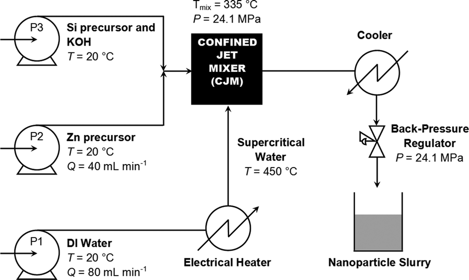 | ||
| Fig. 1 A schematic of the continuous hydrothermal flow synthesis system herein employed. T represents the temperature, Q represents the flow rates of the respective pumps, and P represents the pressure. | ||
Materials characterisation
Powder X-ray diffraction (XRD) data were collected using a STOE Stadi P diffractometer (Mo-Kα radiation source, λ = 0.70932 Å) in transmission geometry. Data collection took place over the 2 theta range 5 to 35°. Scherrer analysis was carried out on the (100), (002), and (102) peaks as detailed elsewhere,36,37 in order to estimate the crystallite size of the nanomaterials. X-ray photoelectron spectroscopy (XPS) was carried out using a Thermo Scientific K-alpha photoelectron spectrometer using monochromatic Al-Kα radiation. Survey scans were collected in the binding energy range 0–1100 eV at a pass energy of 200 eV. Higher resolution scans were recorded for the principal peaks, Zn 2p, Si 2p, O 1s and C 1s at a pass energy of 50 eV. Peak positions were calibrated to carbon using the CasaXPS® software. Transmission electron microscopy (TEM) was carried out using a Jeol 200 kV transmission electron microscope in imaging mode. Powder samples were dispersed in methanol before being drop-coated onto carbon-coated copper TEM grids (Agar Scientific, Stansted, UK). Image and particle size analysis was carried out using Gatan Microscopy Suite® software.Initial assessment of the conductivity of the nanopowders was determined by first pressing ∼0.5 g of each powder into a 16 mm diameter white compact of ∼1 mm thickness under a force of 50 kN using a Specac (Orpington, UK) bench-top hydraulic press. The discs were subsequently heat-treated at 500 °C for 3 h under a 5% H2/N2 atmosphere in a tube furnace (Elite Thermal Systems, Leicestershire, UK). The discs had four gold contacts sputtered onto them and were subjected to an input current of 1 mA and a calibrated magnetic field of 0.58 T using a Van der Pauw probe, as part of an Ecopia HMS-3000 Hall Measurement System, by use of which were obtained the bulk resistivities of the samples. Resistivity measurements were taken in triplicate for each pellet, and three pellets were prepared from each sample. From these, the mean values and standard deviations were calculated.
The dispersion for spin-coating was prepared by first mechanically mixing 20 wt% ethylene glycol with deionised water to be the dispersing medium. The dispersion was comprised of 80 wt% dispersing medium and 20 wt% SiZO powder, and good dispersion was obtained by use of a sonicating tip (Branson Digital Sonifier 250) operating at 20% of full amplitude with a 0.3 s on/off pulse length. A series of ten sonicating treatments with total ‘on’ time of 1 min were carried out in this manner, leaving the dispersion to rest in an ice bath for 2 min between each treatment. Further agitation was carried out in a VWR Ultrasonic Cleaner, USC100T sonicating bath for 30 min before spin coating was carried out using a Laurell Tech. Corp. WS650MZ-23NPPB spin coater onto glass substrates (NSG Pilkingtons, UK) spun at 5000 rpm. The thin films were heat treated at 550 °C for 5 h in a 5% H2/N2 atmosphere. Film thickness measurements were carried out using a Filmetrics F20 Thin Film Analyser. UV/Vis/near-IR reflectance and transmittance spectra were taken using a PerkinElmer Lambda 950 spectrometer using an air background between 300 and 2500 nm, and Hall Probe measurements were carried out as above, with silver paint used to create the four electrical contacts instead of gold sputtering. Scanning electron microscopy (SEM) images were obtained using a JEOL JSM-6700F microscope with a 5 keV accelerating voltage.
Results and discussion
Compositional optimisation
Although TCO compositions with the lowest resistivities in the literature are typically in the range 3 to 7 at% Si,10,11,15 it has previously been shown that ZnO-based CHFS-made TCOs tend to require lower dopant levels to produce materials with low resistivity compared to their non-CHFS analogues.32,33 Thus seven samples of SiZO were first synthesised on the laboratory scale CHFS process at 0.25, 0.5, 1.0, 1.5, 2.0, 2.5, and 3.0 at% Si, respectively (with respect to Zn at% in the starting solution). The optimally conductive sample of 0.25 at% Si, was then synthesised on the pilot scale at a production rate of 350 g h−1. Powder X-ray diffraction patterns for the laboratory scale 0.25, 1.0, and 2.5 at% Si samples are shown in Fig. 2, along with the pattern for 0.25 at% Si synthesised on the pilot scale and a standard pattern for ZnO.38 Each CHFS-made sample had a phase-pure Wurtzite ZnO structure as expected. Scherrer analysis of the (100), (002), and (102) peaks in each XRD pattern, suggested a decrease in crystallite size with the dopant concentration, with values of 28, 24, and 17 nm for the 0.25, 1.0, and 2.5 at% Si samples, respectively, while the crystallite size for 0.25 at% Si synthesised on the pilot scale was calculated to be 26 nm, which is similar (within experimental error) to its laboratory scale analogue.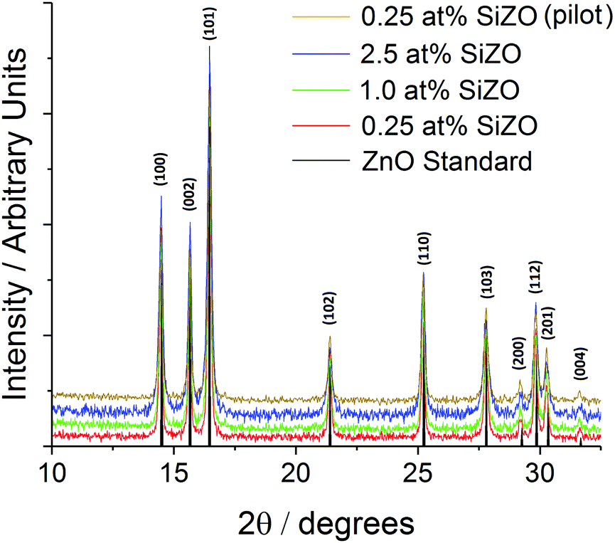 | ||
| Fig. 2 XRD patterns of silicon-doped zinc oxide, including samples with 2.5 at% Si (blue), 1.0 at% Si (green), 0.25 at% Si (red for lab-scale and gold for pilot-scale), and a standard ZnO pattern (black).38 Patterns were acquired from a Mo-Kα source (λ = 0.7093 Å), hence principle peaks appear in the approximate 2θ range 15–30°. | ||
Transmission electron microscopy images are shown in Fig. 3. Although particle morphology across the compositional space explored was variable, the particle size was relatively consistent, particularly at higher dopant levels. Increasing the level of nominal Si-doping reduced the particle size according to the values detailed in Table 1. 0.25 at% Si doping, resulted in considerably larger particles (average particle length of 82.7 nm) than un-doped ZnO (size 32 nm).23 Further doping led to a decrease to 43.8 nm for 1.0 at% Si, and 33.9 nm for 2.5 at% Si (300 particles analysed per sample from TEM images). The aspect ratio was consistently in the range 1.3 to 1.4 for all samples.
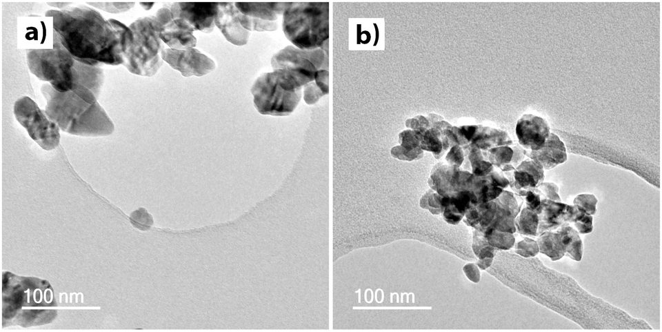 | ||
| Fig. 3 TEM images of silicon-doped zinc oxide. (a) Shows a sample with 0.25 at% Si, while (b) shows a sample with 2.5 at% Si, both at the same magnification. Average particle size was observed to drastically decrease with increasing dopant level. | ||
Due to the low relative sensitivity factor of Si in X-ray photoelectron spectroscopy, Si 2p analysis of samples below 1.0 at% Si did not show any discernible peaks, however quantitative analysis carried out on 1.0 and 2.5 at% Si samples indicated only one Si environment with the Si 2p3/2 peak at 100.8 eV,39 and one Zn environment with the Zn 2p3/2 peak at 1021.2 eV40 for both samples, with approximately a 90% uptake of Si into the structure relative to the nominal Zn![[thin space (1/6-em)]](https://www.rsc.org/images/entities/char_2009.gif) :Si ratio in the precursor solutions. XPS spectra for the Zn 2p and Si 2p regions are included in Fig. S1 of the ESI,† and the key data is summarised in Table 1.
:Si ratio in the precursor solutions. XPS spectra for the Zn 2p and Si 2p regions are included in Fig. S1 of the ESI,† and the key data is summarised in Table 1.
| Sample | BET surface area/m2 g−1 | Scherrer particle size/nm | Mean length/nm | XPS:Si/at% |
|---|---|---|---|---|
| 0.25 at% Si | 12.0 | 28 | 82.7 ± 50.7 | — |
| 1.0 at% Si | 20.8 | 24 | 43.8 ± 17.1 | 0.9 |
| 2.5 at% Si | 27.0 | 17 | 33.9 ± 13.9 | 2.2 |
| 0.25 at% Si (pilot) | 13.4 | 26 | 68.2 ± 37.5 | — |
The samples with nominally 1.0 and 2.5 at% Si in the starting solutions were found to contain 0.9 and 2.2 at% Si, respectively.
The pressed discs of the as-prepared nanomaterials were white in colour, both prior to and after heat-treatment. Their electrical properties are summarised in Table S1 in the ESI,† and displayed visually in Fig. 4. The optimal material in terms of lowest resistivity was the sample with 0.25 at% Si (the lowest dopant level tested) at 3.50 × 10⁻² Ω cm. Note that CHFS-made undoped ZnO pressed and heat-treated in like manner was non-conductive. Increasing the amount of Si dopant increased the resistivity, first slowly then more dramatically. The 0.25 at% Si-doped ZnO was then remade using a pilot scale CHFS at a production rate of 350 g h−1, for which the pressed and heat-treated disk displayed a resistivity of 3.98 × 10⁻² Ω cm, comparable to the analogous material synthesised on the laboratory scale.
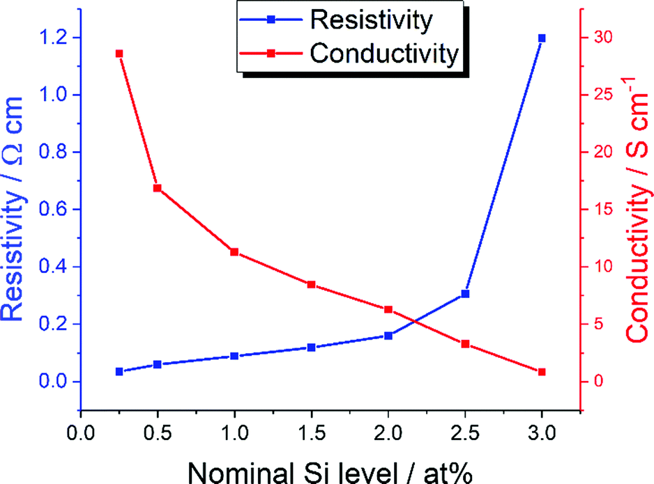 | ||
| Fig. 4 Resistivity (blue) and conductivity (red) data for all compositions of SiZO synthesised on the laboratory scale CHFS. | ||
Thin film deposition and characterisation
Thin films of the 0.25 at% Si-doped ZnO nanopowder synthesised at a rate of 350 g h−1 were prepared using spin coating followed by heat-treatment (detailed in the Experimental section). Filmetrics optical analysis gave an average film thickness of 150 nm (±23 nm). Surface topology was generally featureless and smooth, with good film connectivity as shown by SEM in Fig. 5c. UV/Vis/near-IR data for this film are shown in Fig. 5a; the average visible transmission in the range 400 to 700 nm was 81% (85% transmission at 570 nm). Hall probe measurements gave a minimum resistivity of 2.4 × 10⁻³ Ω cm, with a carrier concentration of 1.02 × 1020 cm−3 and a mobility of 11 cm2 V−1 s−1, a factor of almost twenty times improvement in the resistivity versus the analogous pressed, heat treated pellet. Values for mobility obtained from other SiZO studies varied in the range 10–30 cm2 V−1 s−1,10–13 inherently low due to the two-electron donor dopant scattering effect alluded to in the introduction, and the value of 11 cm2 V−1 s−1 reported herein may have been further hampered by grain boundary effects from imperfect sintering of the nanoparticles during the heat treatment. The carrier concentration and resistivity are within an order of magnitude as thin films of SiZO deposited by other methods. While magnetron sputtering and pulsed laser deposition methods have garnered resistivities in the range 3–9 × 10⁻⁴ Ω cm,10,11,41,42 spray pyrolysis and chemical vapour deposition methods have resulted in higher resistivities of 3.7 × 10⁻³ Ω cm43 and 2.0 × 10⁻² Ω cm,44 respectively, indicating that CHFS manufacture and subsequent spin-coating of SiZO results in films of reasonable electrical properties, with competitive optical properties, and drastically enhanced economy and sustainability of material synthesis and processing.45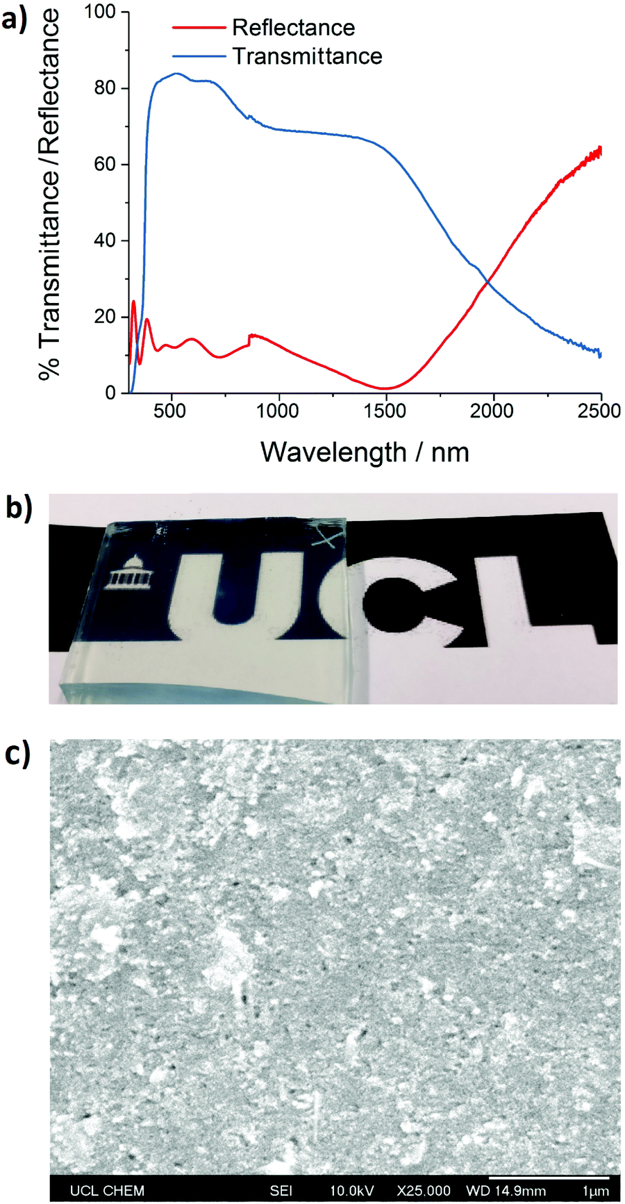 | ||
| Fig. 5 (a) UV/Vis-near-IR transmittance and reflectance data for a spin-coated thin film of 0.25 at% Si-doped ZnO, (b) the ∼2 × 2 cm spin-coated film post heat treatment, from which the spectra were taken, and (c) an SEM image of the surface of the film at ×25000 magnification, the scale bar representative of a distance of 1 μm. The artefact in both spectra in (a) at 860 nm is due to changeover of the lamp in the spectrometer. | ||
Conclusions
In summary, the versatile CHFS process for manufacture of nanoparticle ceramics45 was used for optimising the conductivity of silicon-doped zinc oxide nanopowders. Comparison of the compositions was carried out by use of Hall Effect measurements on pressed, heat-treated pellets of the powders. It was found that the lowest nominal dopant level of silicon tested, (0.25 at% Si with respect to 99.75 at% Zn), had the lowest resistivity of 3.50 × 10⁻² Ω cm. The material was successfully scaled up from 60 to 350 g h−1 by going from the laboratory-scale to a pilot-scale CHFS process, with retention of the electrical properties. The 0.25 at% Si doped ZnO made on the pilot plant CHFS process was made into a thin film via spin coating and heat-treatment, yielding a resistivity of 2.4 × 10⁻³ Ω cm with an average visible light transmission of 81%, hitherto the most conductive thin film ever reported from CHFS-made nanoparticles.Acknowledgements
The EPSRC are thanked for funding Award 1480036 (DPH) and the “Sustainable Manufacturing of Transparent Conducting Oxide (TCO) Inks and Thin Films” project, EP/L017709/1 (PM, CJC, IPP, JAD).References
- C. Granqvist, A. Azens, A. Hjelm, L. Kullman, G. Niklasson, D. Rönnow, M. S. Mattson, M. Veszelei and G. Vaivars, Sol. Energy, 1998, 63, 199–216 CrossRef CAS.
- S. Calnan and A. Tiwari, Thin Solid Films, 2010, 518, 1839–1849 CrossRef CAS.
- K. Chopra, S. Major and D. Pandya, Thin Solid Films, 1983, 102, 1–46 CrossRef CAS.
- T. Minami, Semicond. Sci. Technol., 2005, 20, S35 CrossRef CAS.
- J.-W. Park, G.-H. Lee, Y. Y. Kwon, K.-W. Park, J. Lee, W. Jin, Y.-C. Nah and H. Kim, Org. Electron., 2014, 15, 2178–2183 CrossRef CAS.
- R. G. Gordon, MRS Bull., 2000, 25, 52–57 CrossRef CAS.
- United States Geological Survey Mineral Commodity Summaries (2004–2016), http://https://minerals.usgs.gov/minerals/pubs/commodity/indium/ (accessed 10/04/2017).
- A. Stadler, Materials, 2012, 5, 661–683 CrossRef.
- P. P. Edwards, A. Porch, M. O. Jones and D. V. Morgan, Dalton Trans., 2004, 2995–3002 RSC.
- Q. Hua, W. Ligang, L. Ruijin and Y. Wenfeng, Optik, 2014, 125, 3902–3907 CrossRef CAS.
- A. K. Das, P. Misra and L. M. Kukreja, J. Phy. D: Appl. Phys., 2009, 42(165405), 1–7 Search PubMed.
- I. Sorar, D. Saygin-Hinczewski, M. Hinczewski and F. Z. Tepehan, Appl. Surf. Sci., 2011, 257, 7343–7349 CrossRef CAS.
- H. Qin, H. F. Liu and Y. Z. Yuan, Surf. Eng., 2013, 29, 70–76 CrossRef CAS.
- G. Bajpai, T. Srivastava, M. Nasir, S. Tiwari, S. Bajpai, E. G. Rini, S. Biring and S. Sen, Scr. Mater., 2017, 135, 1–4 CrossRef CAS.
- V. L. Kiznetsov, A. T. Vai, M. Al-Mamouri, J. S. Abell, M. Pepper and P. P. Edwards, Appl. Phys. Lett., 2015, 107(232103), 1–5 Search PubMed.
- S. Kumar and B. Sarkar, International Journal of Current Engineering Technology, 2013, 3, 123–128 CAS.
- Z. C. Chang, International Journal of Chemical, Molecular, Nuclear, Materials and Metallurgical Engineering, 2015, 9, 725–730 Search PubMed.
- S. Cimitan, S. Albonetti, L. Forni, F. Peri and D. Lazzari, J. Colloid Interface Sci., 2009, 329, 73–80 CrossRef CAS PubMed.
- J. Lu, K. Minami, S. Takami, M. Shibata, Y. Kaneko and T. Adschiri, ACS Appl. Mater. Interfaces, 2012, 4, 351–354 CAS.
- M. Ohyama, H. Kouzuka and T. Yoko, Thin Solid Films, 1997, 306, 78–85 CrossRef CAS.
- A. F. Aktaruzzaman, G. L. Sharma and L. K. Malhotra, Thin Solid Films, 1991, 198, 67–74 CrossRef CAS.
- J. Bogdan, J. Zarzyńska and J. Pławińska-Czarnak, Nanoscale Res. Lett., 2015, 10(57), 1–10 Search PubMed.
- J. B. M. Goodall, D. Illsley, R. Lines, N. M. Makwana and J. A. Darr, ACS Comb. Sci., 2015, 17, 100–112 CrossRef CAS PubMed.
- I. D. Johnson, M. Lübke, O. Y. Wu, N. M. Makwana, G. J. Smales, H. U. Islam, R. Y. Dedigama, R. I. Gruar, C. J. Tighe, D. O. Scanlon, F. Corà, D. J. Brett, P. R. Shearing and J. A. Darr, J. Power Sources, 2016, 302, 410–418 CrossRef CAS.
- M. Lübke, D. Howard, C. F. Armer, A. J. Gardecka, A. Lowe, M. V. Reddy, Z. Liu and J. A. Darr, Electrochim. Acta, 2017, 231, 247–254 CrossRef.
- H.-S. Hwang, B.-Y. Jeong, J. Moon, S.-K. Chun and J. Kim, Mater. Sci. Eng., B, 2011, 176, 1128–1131 CrossRef.
- S. Vunnam, K. Ankireddy, J. Kellar and W. Cross, Nanotechnology, 2014, 25(195301), 1–9 Search PubMed.
- E. Della Gaspera, M. Bersani, M. Cittadini, M. Guglielmi, D. Pagani, R. Noriega, S. Mehra, A. Salleo and A. Martucci, J. Am. Chem. Soc., 2013, 135, 3439–3448 CrossRef PubMed.
- R. A. Street, W. Wong, S. Ready, M. Chabinye, A. Arias, S. Limb, A. Salleo and R. Lujan, Mater. Today, 2006, 9, 32–37 CrossRef CAS.
- N. Al-Dahoudi and M. A. Aegerter, J. Sol–Gel Sci. Technol., 2003, 26, 693–697 CrossRef CAS.
- P. Marchand, N. M. Makwana, C. J. Tighe, R. I. Gruar, I. P. Parkin, C. J. Carmalt and J. A. Darr, ACS Comb. Sci., 2016, 18, 130–137 CrossRef CAS PubMed.
- D. P. Howard, P. Marchand, I. D. Johnson, C. J. Carmalt, I. P. Parkin and J. A. Darr, J. Mater. Chem. A, 2016, 4, 12774–12780 CAS.
- D. P. Howard, P. Marchand, L. McCafferty, C. J. Carmalt, I. P. Parkin and J. A. Darr, ACS Comb. Sci., 2017, 19, 239–245 CrossRef CAS PubMed.
- J. A. Darr, C. J. Tighe and R. I. Gruar, US Pat., 9192901, 2015 Search PubMed.
- W. Wagner and A. Pruß, J. Phys. Chem. Ref. Data, 2002, 31, 387–535 CrossRef CAS.
- A. Patterson, Phys. Rev., 1939, 56, 978–982 CrossRef CAS.
- L. J. van der Pauw, Philips Res. Rep., 1958, 13, 1–9 Search PubMed.
- H. Schulz and K. Thiemann, Solid State Commun., 1979, 32, 783–785 CrossRef CAS.
- W. A. M. Aarnik, A. Weishaupt and A. van Silfout, Appl. Surf. Sci., 1990, 45, 37–48 CrossRef.
- B. R. Strohmeier and D. M. Hercules, J. Catal., 1984, 86, 266–279 CrossRef CAS.
- J. Clatot, M. Nistor and A. Rougier, Thin Solid Films, 2013, 531, 197–202 CrossRef CAS.
- R. E. Treharne, L. J. Phillips, K. Durose, A. Weerakkody, I. Z. Mitrovic and S. Hall, J. Appl. Phys., 2014, 115(063505), 1–7 Search PubMed.
- N. Rashidi, V. L. Kuznetsov, J. R. Dilworth, M. Pepper, P. J. Dobson and P. P. Edwards, J. Mater. Chem. C, 2013, 1, 6960–6969 RSC.
- D. B. Potter, M. J. Powell, J. A. Darr, I. P. Parkin and C. J. Carmalt, RSC Adv., 2017, 7, 10806–10814 RSC.
- J. A. Darr, J. Zhang, N. M. Makwana and X. Weng, Chem. Rev., 2017 DOI:10.1021/acs.chemrev.6b00417.
Footnote |
| † Electronic supplementary information (ESI) available. See DOI: 10.1039/c7tc02175e |
| This journal is © The Royal Society of Chemistry 2017 |