
 Open Access Article
 This Open Access Article is licensed under a Creative Commons Attribution-Non Commercial 3.0 Unported Licence
Rapid laser-induced photochemical conversion of sol–gel precursors to In2O3 layers and their application in thin-film transistors†
Spilios
Dellis
 a,
Ivan
Isakov
b,
Nikolaos
Kalfagiannis
a,
Kornelius
Tetzner
b,
Thomas D.
Anthopoulos
b and
Demosthenes C.
Koutsogeorgis
*a
a,
Ivan
Isakov
b,
Nikolaos
Kalfagiannis
a,
Kornelius
Tetzner
b,
Thomas D.
Anthopoulos
b and
Demosthenes C.
Koutsogeorgis
*a
aDepartment of Physics, School of Science and Technology, Nottingham Trent University, Nottingham, NG11 8NS, UK. E-mail: demosthenes.koutsogeorgis@ntu.ac.uk
bDepartment of Physics and Centre for Plastic Electronics, Imperial College London, London, SW7 2AZ, UK
First published on 22nd March 2017
Abstract
We report the development of indium oxide (In2O3) transistors via a single step laser-induced photochemical conversion process of a sol–gel metal oxide precursor. Through careful optimization of the laser annealing conditions we demonstrated successful conversion of the precursor to In2O3 and its subsequent implementation in n-channel transistors with electron mobility up to 13 cm2 V−1 s−1. Importantly, the process does not require thermal annealing making it compatible with temperature sensitive materials such as plastic. On the other hand, the spatial conversion/densification of the sol–gel layer eliminates additional process steps associated with semiconductor patterning and hence significantly reduces fabrication complexity and cost. Our work demonstrates unambiguously that laser-induced photochemical conversion of sol–gel metal oxide precursors can be rapid and suitable for the manufacturing of large-area electronics.
Thin-film transistors (TFTs) based on transparent metal oxide semiconductors hold great promise for a variety of emerging applications in large-area/volume electronics, including, but not limited to, flexible displays,1 radio frequency identification (RFID) tags,2 and transparent electronic devices.3 To this end, recent years have witnessed the development of a wide range of high-mobility metal oxide semiconductors and devices that can be manufactured over large areas employing simple fabrication methods.4 Among the various deposition techniques demonstrated, solution processing offers a scalable and cost effective route for high throughput and large-area deposition of various oxide materials including ZnO, In2O3, In4ZnO, and InGaZnO (IGZO).5,6
Despite the huge promise, however, accurate control over the morphology and the chemical composition of solution-grown metal-oxides still remains challenging, leading to significant device-to-device performance variations. In addition, deposition of semiconducting metal oxides by “sol–gel” has so far been limited to high processing temperatures, typically in excess of >350 °C, rendering the technology incompatible with inexpensive, temperature-sensitive substrates such as plastic, the material of choice for large-scale roll-to-roll (R2R) processes.7–9 This post-deposition heat treatment is a major obstacle that hinders the integration of heat-sensitive flexible polymeric substrates. Therefore, it is essential to develop alternative methods of processing that can meet the demands relevant to this area. Thermal annealing at reduced processing temperature, ideally less than 150 °C, has been examined aiming at oxide TFTs fabrication on flexible polymeric substrates.10 However, the processing times that are typically required are very long (up to 4 h) and the achieved TFTs performance and stability are largely inadequate for real electronic applications.11
Optical annealing can be viewed as a powerful tool towards low-temperature fabrication schemes, however, recent reports on optical sintering suffer from lengthy exposure that renders the process unsuitable for high throughput R2R manufacturing.9 Therefore, alternative methods that can deliver rapid and scalable materials processing are urgently required.12 To this end, Laser Annealing (LA) offers fast processing along with rapid, precise and selective energy delivery in area and depth via critical laser energy absorption.13,14 For instance, it has been shown that the use of ultrashort ultraviolet (UV) laser pulses can result in a significant enhancement of the electronic properties of the semiconductor, which in many cases cannot be achieved with conventional annealing.15
Despite the tremendous potential, however, to date only few studies have reported the use of LA for the fabrication/post-processing of metal oxide thin films. Imai et al.16 showed that a high number of low fluence laser pulses (up to 1800 pulses of 20 mJ cm−2) produced from an ArF excimer laser (193 nm) were able to remove organic compounds and induce crystallization in numerous initially amorphous metal oxide films. Low-fluence/multiple-pulse LA with XeCl excimer laser (308 nm) was suggested by Yang et al. in the fabrication of IGZO TFTs resulting in a field-effect mobility of 7.65 cm2 V−1 s−1.8 A different approach was recommended by Tsay et al. where the researchers employed high fluence and a low number of pulses (15) from a KrF excimer laser (248 nm) for improving the physical properties of IGZO thin film.17
In2O3 is a wide band-gap semiconducting material with great perspectives in the transparent electronics technology as it exhibits both high optical transparency and superior electronic properties with electron mobility of up to 220 cm2 V−1 s−1 reported for single crystals.18–21 For this reason, a number of studies on the fabrication of In2O3 TFTs using high-temperature thermal annealing or a combination of thermal and optical annealing have been reported in recent years.9,12,22,23 Here, we describe the fabrication of fully functional and high performance n-channel In2O3 TFTs, via LA in ambient atmosphere. During the laser-induced photo-conversion process, the sample temperature never exceeds the 150 °C, making the proposed approach compatible with plastic substrates. Despite the low thermal budget, the resulting TFTs exhibit excellent operating characteristics with electron mobility values of up to 13 cm2 V−1 s−1.
Doped silicon (Si-n++) wafers with a thermally grown 400 nm-thick layer of SiO2 acting as gate and gate dielectric respectively, were used for the fabrication of bottom-gate, top-contact transistors (BG-TC). Prior to the deposition of the In2O3 layer, the substrates were cleaned by ultrasonication in deionized water, acetone, and isopropanol (IPA), with each step lasting 10 min. Substrates were subsequently exposed to atmospheric pressure UV ozone treatment for 10 min at room temperature. The metal oxide precursor solution consisted of indium nitrate (In(NO3)3) and 2-methoxyethanol (2-ME) with a concentration of 20 mg ml−1 and was spun-coated directly on the Si++/SiO2 substrates for 30 s at 4000 rpm (Fig. 1b(i)). As-spun precursor layers were thermally stabilised by drying them on a hot-plate at 150 °C for 15 min in order to remove excessive solvent residues.24 LA (Fig. 1b(ii)) was carried out with a KrF Excimer laser (LAMBDA PHYSIK LPX 305i), which is capable of delivering 25 ns pulses of unpolarized light at 248 nm with energy up to 1200 mJ per pulse. The beam delivery system (Fig. 1a) comprises a variable attenuator, a beam homogenizer and a mask projection system. An XYZ translational stage was used in order to manipulate the sample during the laser processing. The laser spot delivered onto the samples was set to be a 2.5 × 2.5 mm2 spot, with fluence (energy density) uniformity better than 2% throughout the spot. An extensive experimental schedule was followed, varying the number of pulses (1 to 10 at 1 Hz repetition rate) and the fluence (100–450 mJ cm−2 with a step of 50 mJ cm−2). After the LA step, TFT fabrication was completed with the thermal evaporation of the aluminum source and drain electrodes in high vacuum (<10−5 mbar) using shadow masks (Fig. 1b(iii)). The width and length of the TFT channels were 11 mm and 100 μm, respectively. TFT characterization was carried out in a nitrogen atmosphere (samples maintained at room temperature) using an Agilent B2902A parameter analyser. The field-effect electron mobility was extracted from the linear operating regime using the gradual channel approximation according to:
 | (1) |
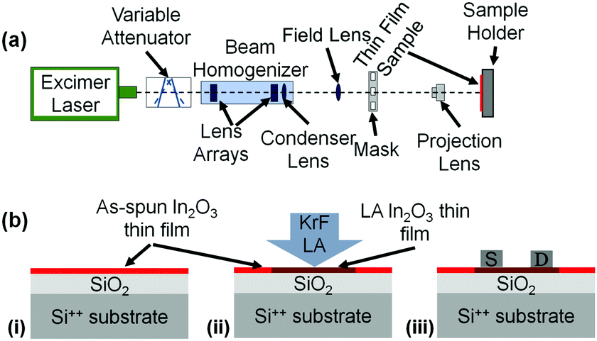 | ||
| Fig. 1 (a) The LA experimental setup used in the present work. (b) Schematic representation of the fabrication process of BG-TC In2O3 TFTs on Si/SiO2 substrates. | ||
The as-spun In2O3 (after stabilization at 150 °C for 15 min) exhibits an insulating character that remained unaffected even after applying up to 10 pulses of fluence lower than 300 mJ cm−2. Fig. 2 displays the transfer characteristics of LA In2O3 TFTs prepared with 10 pulses at 300 mJ cm−2. The device exhibits electron transport (n-channel) behavior with threshold voltage (Vth) of approximately −60 V and onset voltage (VON) below −100 V (minimum range measured). For the devices fabricated with fluence up to 400 mJ cm−2, Vth is in the range of −25 to −120 V and remains relatively constant with higher number of pulses (Fig. 3a). Above 450 mJ cm−2, however, Vth progressively shifts to more negative values, turning the film severely conductive at higher number of pulses. Transfer characteristics of all the TFT devices prepared in his work, before and after the mild thermal treatment, are presented in Fig. S1 of the ESI.†
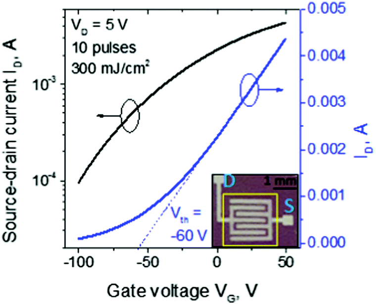 | ||
| Fig. 2 Transfer characteristics of the LA In2O3 TFTs (10 pulses at 300 mJ cm−2); inset: optical micrograph of a complete device showing drain and source contacts and outline of the area subjected to LA. | ||
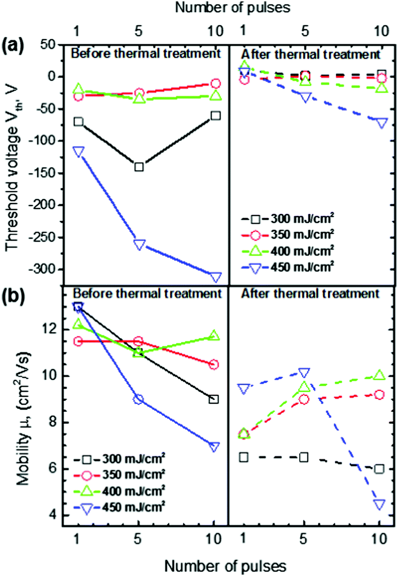 | ||
| Fig. 3 (a) Threshold voltage and (b) mobility of the LA In2O3 TFTs before (solid lines) and after (dashed lines) the post fabrication mild-thermal treatment at 100 °C for different LA processing. The lines in this figure serve only as a guide to the eyes. | ||
Fig. 3b shows the field-effect mobility measured in the linear regime for all LA In2O3 TFTs. All the devices exhibit high mobility with typical values in the range 9–13 cm2 V−1 s−1. These results highlight the tremendous potential of LA as an alternative processing route for the development of metal oxide TFTs.
A potential drawback of LA of In2O3 is the large negative Vth observed in all TFTs, as it can lead to high power consumption. To address this an additional process step was implemented in order to shift Vth towards VG = 0 V. The step comprises of a mild thermal annealing of the TFTs following complete fabrication (to include source and drain electrodes), during which the samples were heated to 100 °C for 60 min. Post-annealed devices showed Vth much closer to zero, especially for devices below 400 mJ cm−2, albeit accompanied with a slight reduction in electron mobility, as shown in Fig. 3a and b respectively. The transfer and output characteristics of the LA In2O3 TFT (10 pulse at 300 mJ cm−2, the same device shown in Fig. 2) with mild post-fabrication thermal annealing are presented in Fig. 4. As can be seen, the Vth and VON shift to +5 V and −60 V, respectively. In this case the VG range was sufficient for studying the TFT performance in both on and off-state and allowed the ION/IOFF to be calculated as higher than 106. This further thermal treatment step is not expected to affect the ION/IOFF but only to shift the Vth to more positive values. The μ is found to marginally decrease, probably due to the device not reaching its maximum mobility at the gate-voltages used. These trends are representative for all LA In2O3 TFTs with average ION/IOFF ratio of >105, Vth close to zero, and μ in the range of 6–10 cm2 V−1 s−1. Output characteristics shown in Fig. 4b indicate Ohmic-like injecting behavior, negligible gate leakage in the low voltage regime and saturation regime at high voltages.
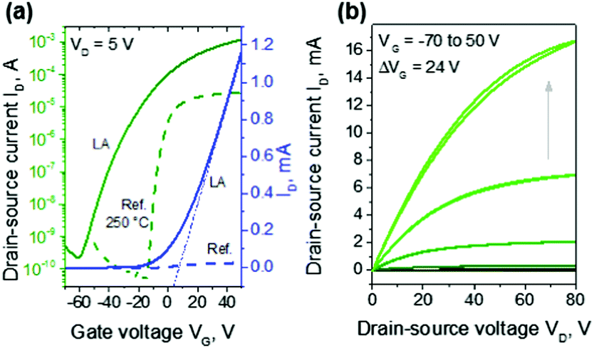 | ||
| Fig. 4 (a) Transfer characteristics of the LA In2O3 TFT (10 pulses at 300 mJ cm−2) after the mild-thermal treatment. For comparison the transfer characteristics of the reference device are also shown (dashed lines); (b) output curves of the same device. | ||
In2O3 TFT devices were also prepared by thermal annealing at 250 °C for 60 min, as a reference for comparison (Fig. 4a, dashed lines). Although the VON of the devices and their sub-threshold slope were superior to the LA ones, the μ values were significantly lower and in the order of 0.4 cm2 V−1 s−1. This relatively low μ value as compared to previously published data,24 could be the result of the prolonged exposure of In2O3 to non-controlled environment; all samples were exposed to ambient air for 2 weeks during LA of the In2O3 layers, S–D deposition and electrical characterization.9 Therefore, an overall device process optimization is expected to lead to significantly improved TFT performance. Despite the nonidealities, the average μ obtained for LA In2O3 TFTs is very high if one considers the low thermal budget and very high speed of the process.
High resolution XPS spectra of In2O3 films were collected and analysed in order to confirm the quality and chemical composition of the resulting films. Wide XPS scans (presented in Fig. S2 and Table S1 of the ESI†) were obtained for the as-spun, thermal annealed at 250 °C for 60 min (reference), and laser annealed (10 pulses of 300 mJ cm−2) with and without post-thermal treatment at a mild temperature (100 °C for 60 min). These spectra were used for the calculation of the ratio between the atomic concentration of In and O on the surface of the films. The as-spun film (only with a short time baking at 150 °C for 15 min) presents a [O]/[In] concentration ratio of 2.24 that reduces to 2.09 for the film that was thermally annealed at 250 °C for 60 min, a value very close to the atomic concentration ratio of [O]/[In] presented by H. Faber et al.22 Laser annealing with 10 pulses of 300 mJ cm−2 leads approximately to the same atomic concentration ratio (2.00), but is further reduced after the mild post-thermal treatment to reach 1.83.
Different types of oxygen bonds in the In2O3 films were identified by analysis of the high resolution O 1s XPS peaks, as they are very sensitive indicators of bonds between oxygen and other elements and they can be used to distinguish between different contributions to the overall oxygen signal recorded in the wide range XPS scans. In all cases (see Fig. 5) the O 1s peak envelope can be deconvoluted to three peaks located at 529.5 eV (In–O bonds in In2O3), 530.2 eV (O adsorbates on the surface), and 532.0 eV (water and In–OH bonds).22,25,26 The extent of the initial precursor's conversion to metal oxide can be evaluated by the ratio found between In–O to In–OH bonds.27,28 As shown in Fig. 5a (as well as in Table S2 of the ESI†) the as-spun sample exhibits higher proportion of In–OH bonds compared to In–O bonds. This is reduced with thermal annealing at 250 °C for 60 min. However, it is reversed with laser annealing resulting to a higher proportion of In–O bonds rather than In–OH bonds. This reversal is then boosted further with the mild thermal treatment of 100 °C for 60 min. Finally, the as-spun In2O3 film (after spin-coating and short time baking at 150 °C for 15 min) presents an optical band-gap of 4.04 eV (as derived from Tauc plot method,29 which is presented in Fig. S5 of the ESI†); thus it is expected to absorb the photons of the KrF excimer laser that have an energy of 5 eV, leading to an increase of its temperature, inducing the removal of the solvent.27,28 Based on this mechanism and on the above results regarding the chemical composition of the In2O3 thin films, the improved TFT characteristics via LA may well be attributed to a more efficient solvent removal and precursor conversion, possibly due to the highly localised and ultra-rapid heating compared to traditional thermal treatment. The ratio of [In–O]/[In–OH] was found to be 1.10 and 1.27 with LA (without and with the mild thermal treatment, respectively), whereas it was only 0.64 with thermal annealing at 250 °C for 60 min.
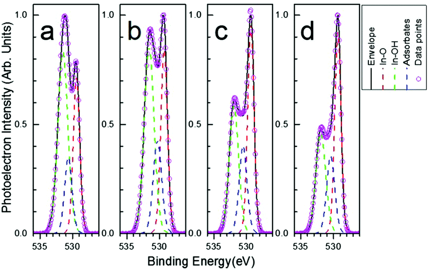 | ||
| Fig. 5 High-resolution O 1s spectra of indium oxide thin films (a) as-spun, (b) thermally annealed at 250 °C for 60 min, (c) laser annealed with 10 pulses of 300 mJ cm−2, and (d) laser annealed with 10 pulses of 300 mJ cm−2 followed by thermal annealing at 100 °C for 60 min. Together with the experimental data, plots include the deconvolution into In–O (red dashed line), In–OH (green dashed line), and O adsorbates (blue dashed line) peaks. | ||
Another advantage of the LA process is the removal of the necessity of any In2O3 patterning step. The latter is a common practice for all metal oxide TFTs fabricated by conventional non-additive deposition techniques, including vacuum and solution-phase processes, in order to electrically isolate the individual device.22 Unlike traditional methods, LA can be performed on-demand on selected areas of the substrate. Upon LA, only the irradiated area of the precursor film is converted from a soluble insulating state to an insoluble metal oxide semiconductor, leaving the rest of the sol–gel film unaffected. As a consequence, the resulting TFTs exhibit very low gate leakage current that is typically around 10−10 A (our measurement limit). The gate leakage current of In2O3 TFTs prepared by conventional high-temperature thermal annealing and by laser annealing (with and without mild-thermal treatment following the LA), and without any device patterning are presented in Fig. S6 of ESI.† Such low leakage current is critical for the successful implementation of any TFT technology in commercial electronic products. Furthermore, the unconverted regions of the sol–gel layer can be easily removed by immersing the entire substrate to a suitable solvent bath. Although not relevant to this work, such simplified direct patterning process could well be exploited in the future for the manufacturing of complementary circuitry involving patterning of p- and n-channel TFTs in close proximity to each other on the same substrate, as a substitution for an elaborate and hence costly conventional patterning process.
In summary, we demonstrated the application of laser annealing for the rapid chemical conversion of a metal oxide sol–gel precursor to a high electron mobility semiconductor and its subsequent implementation in n-channel In2O3 TFTs. Key characteristics of the LA process include: (i) solution deposition of the precursor sol–gel material, (ii) high speed chemical conversion of the precursor to the semiconducting state via controlled LA, and (iii) low thermal budget that does not exceed 150 °C during any stage of the fabrication process. Additionally, the localized and selective character of the LA process allows for the spatial conversion of the precursor layer to semiconductor, leaving the unexposed sol–gel layer in its insulating state. This leads to TFTs with extremely low gate leakage current, an attribute that can only be otherwise achieved through the introduction of additional, and hence costly, semiconductor patterning steps. Finally, the proposed LA process does not rely on controlled atmosphere, hence further simplifying its application and potential scale up.
Acknowledgements
This work was conducted under the Pathfinder project LAFLEXEL, that was funded by the Centre of Innovative Manufacturing for Large Area Electronics (CIMLAE) and hence in extension by the EPSRC. K. T. and T. D. A. also acknowledge financial support from the People Programme (Marie Curie Actions) of the European Union's Framework Programme Horizon2020: “Flexible Complementary Hybrid Integrated Circuits” (FlexCHIC), grant agreement no. 658563.References
- J. K. Jeong, Semicond. Sci. Technol., 2011, 26, 34008 CrossRef.
- A. Nathan, A. Ahnood, M. T. Cole, S. Lee, Y. Suzuki, P. Hiralal, F. Bonaccorso, T. Hasan, L. Garcia-Gancedo, A. Dyadyusha, S. Haque, P. Andrew, S. Hofmann, J. Moultrie, D. Chu, A. J. Flewitt, A. C. Ferrari, M. J. Kelly, J. Robertson, G. A. J. Amaratunga and W. I. Milne, Proc. IEEE, 2012, 100, 1486–1517 CrossRef.
- L. Petti, N. Munzenrieder, C. Vogt, H. Faber, L. Buthe, G. Cantarella, F. Bottacchi, T. D. Anthopoulos and G. Troster, Appl. Phys. Rev., 2016, 21303, 1–57 Search PubMed.
- Y. Sun and J. A. Rogers, Adv. Mater., 2007, 19, 1897–1916 CrossRef CAS.
- P. F. Moonen, I. Yakimets and J. Huskens, Adv. Mater., 2012, 24, 5526–5541 CrossRef CAS PubMed.
- S. R. Thomas, P. Pattanasattayavong and T. D. Anthopoulos, Chem. Soc. Rev., 2013, 42, 6910 RSC.
- K. K. Banger, R. L. Peterson, K. Mori, Y. Yamashita, T. Leedham and H. Sirringhaus, Chem. Mater., 2014, 26, 1195–1203 CrossRef CAS PubMed.
- Y.-H. Yang, S. S. Yang and K.-S. Chou, IEEE Electron Device Lett., 2010, 31, 969–971 CrossRef CAS.
- Y.-H. Kim, J.-S. Heo, T.-H. Kim, S. K. Park, M.-H. Yoon, J. Kim, M. S. Oh, G.-R. Yi, Y.-Y. Noh and S. K. Park, Nature, 2012, 489, 128–132 CrossRef CAS PubMed.
- S. Yang, J. Y. Bak, S. Yoon, M. K. Ryu, H. Oh, C. Hwang, G. H. Kim, S. K. Park and J. Jang, IEEE Electron Device Lett., 2011, 32, 1692–1694 CrossRef CAS.
- G. J. Lee, J. Kim, J.-H. Kim, S. M. Jeong, J. E. Jang and J. Jeong, Semicond. Sci. Technol., 2014, 29, 35003 CrossRef.
- J. Leppäniemi, K. Ojanperä, T. Kololuoma, O.-H. Huttunen, J. Dahl, M. Tuominen, P. Laukkanen, H. Majumdar and A. Alastalo, Appl. Phys. Lett., 2014, 105, 113514 CrossRef.
- N. Kalfagiannis, A. Siozios, D. V. Bellas, D. Toliopoulos, L. Bowen, N. Pliatsikas, W. M. Cranton, C. Kosmidis, D. C. Koutsogeorgis, E. Lidorikis and P. Patsalas, Nanoscale, 2016, 8, 8236–8244 RSC.
- C. Tsakonas, W. Cranton, F. Li, K. Abusabee, A. Flewitt, D. Koutsogeorgis and R. Ranson, J. Phys. D: Appl. Phys., 2013, 46, 95305 CrossRef.
- M. Nakata, K. Takechi, T. Eguchi, E. Tokumitsu, H. Yamaguchi and S. Kaneko, Jpn. J. Appl. Phys., 2009, 48, 81608 CrossRef.
- H. Imai, A. Tominaga, H. Hirashima, M. Toki and N. Asakuma, J. Appl. Phys., 1999, 85, 203–207 CrossRef CAS.
- C. Y. Tsay and T. T. Huang, Mater. Chem. Phys., 2013, 140, 365–372 CrossRef CAS.
- Z. Galazka, R. Uecker and R. Fornari, J. Cryst. Growth, 2014, 388, 61–69 CrossRef CAS.
- O. Bierwagen and J. S. Speck, Appl. Phys. Lett., 2010, 97, 97–100 CrossRef.
- R. L. Weiher, J. Appl. Phys., 1962, 33, 2834–2839 CrossRef CAS.
- K. Nomura, H. Ohta, A. Takagi, T. Kamiya, M. Hirano and H. Hosono, Nature, 2004, 432, 488–492 CrossRef CAS PubMed.
- H. Faber, Y.-H. Lin, S. R. Thomas, K. Zhao, N. Pliatsikas, M. A. McLachlan, A. Amassian, P. A. Patsalas and T. D. Anthopoulos, ACS Appl. Mater. Interfaces, 2015, 7, 782–790 CAS.
- L. Petti, H. Faber, N. Münzenrieder, G. Cantarella, P. A. Patsalas, G. Tröster and T. D. Anthopoulos, Appl. Phys. Lett., 2015, 106, 92105 CrossRef.
- Y.-H. Lin, H. Faber, J. G. Labram, E. Stratakis, L. Sygellou, E. Kymakis, N. A. Hastas, R. Li, K. Zhao, A. Amassian, N. D. Treat, M. McLachlan and T. D. Anthopoulos, Adv. Sci., 2015, 2, 1500058 CrossRef PubMed.
- J. F. Moulder, W. F. Stickle, P. E. Sobol and K. D. Bomben, Surf. Interface Anal., 1979, 3, v–v Search PubMed.
- A. Gurlo, M. Ivanovskaya, A. Pfau, U. Weimar and W. G. Spel, Thin Solid Films, 1997, 307, 288–293 CrossRef CAS.
- S. Park, K.-H. Kim, J.-W. Jo, S. Sung, K.-T. Kim, W.-J. Lee, J. Kim, H. J. Kim, G.-R. Yi, Y.-H. Kim, M.-H. Yoon and S. K. Park, Adv. Funct. Mater., 2015, 25, 2807–2815 CrossRef CAS.
- J. Hwang, K. Lee, Y. Jeong, Y. U. Lee, C. Pearson, M. C. Petty and H. Kim, Adv. Mater. Interfaces, 2014, 1, 1–9 Search PubMed.
- J. Tauc, R. Grigorovici and A. Vancu, Phys. Status Solidi, 1966, 15, 627–637 CrossRef CAS.
Footnote |
| † Electronic supplementary information (ESI) available. See DOI: 10.1039/c7tc00169j |
| This journal is © The Royal Society of Chemistry 2017 |