
 Open Access Article
 This Open Access Article is licensed under a
 Creative Commons Attribution 3.0 Unported Licence
Switchable disposable passive RFID vapour sensors from inkjet printed electronic components integrated with PDMS as a stimulus responsive material†
K. E.
Belsey
a,
A. V. S.
Parry
 b,
C. V.
Rumens
a,
M. A.
Ziai
c,
S. G.
Yeates
*b,
J. C.
Batchelor
*c and
S. J.
Holder
*a
b,
C. V.
Rumens
a,
M. A.
Ziai
c,
S. G.
Yeates
*b,
J. C.
Batchelor
*c and
S. J.
Holder
*a
aFunctional Materials Group, School of Physical Sciences, University of Kent, Canterbury, Kent CT2 7NH, UK. E-mail: S.J.Holder@kent.ac.uk
bSchool of Chemistry, University of Manchester, Manchester, M13 9PL, UK. E-mail: Steven.Yeates@manchester.ac.uk
cSchool of Engineering and the Digital Arts, University of Kent, Canterbury, Kent CT2 7NT, UK. E-mail: J.C.Batchelor@kent.ac.uk
First published on 2nd March 2017
Abstract
A route to cheap and disposable sensors for the chemical sensing market, with potential applications including monitoring of food spoilage, is reported herein. The sensor is the result of the direct integration of a stimuli-responsive material, poly(dimethylsiloxane) (PDMS), with an electronic component. The printing and sintering of colloidal silver ink solutions onto PDMS was optimized to allow the printing of conductive silver feed loops, which are the active sensing component in antennas for passive (battery-free) Radio Frequency Identification (RFID) tags. The response of these devices is related to the degree of swelling of the PDMS, which, in turn, has been shown to be correlated to the Hansen solubility parameters and the vapour pressures of the corresponding volatile organic compounds (VOCs). When exposed to solvent vapour the printed feed loop fractures, increasing resistance and ultimately breaking conductivity, leading to a change in the transmitted power and read range of the wireless device. Remarkably upon removal from the vapour, the fractured feed loops reassemble and become conductive again, making them switchable and “multi-use”. This work paves the way to a fully inkjet printed RFID substrate for vapour detection.
1. Introduction
Wireless sensors will be one of the major facilitating technologies in the development and progression of the paradigm of the Internet of Things.1 In particular the concept and application of label based chemical sensing using Radio Frequency Identity (RFID) tags will be key to the routine wireless chemical monitoring of the environment around these labels.2 Such labels already have applications in the transport, health and safety, environmental and food industries and wireless sensing for these and other applications will expand provided costs can be reduced. For example the monitoring of individual perishable food products requires cheap disposable RFID labels that can be integrated into food packaging and that can be easily interrogated by simple wireless devices.3 To facilitate this demand such RFID tags should ideally be passive (i.e. possess no intrinsic power supply), be readily manufactured on a large scale (for example through additive manufacturing technologies such as printing) and involve cheap integral components.4 The sensing material (typically stimulus responsive) integrated into or onto the antenna similarly needs to be amenable to simple additive manufacturing and must not be unduly expensive. In particular a unique responsive material utilized for each individual type of foodstuff packaging is not attractive. In principle an existing material that can be immediately utilized or readily chemically ‘tweaked’ for general categories of foodstuff monitoring would be ideal.Previous work on RFID sensors has seen the incorporation of stimulus responsive materials into a range of antenna designs with a significant number of these in recent years being passive.5 A number of approaches to humidity sensing have been reported where varying degrees of specificity of the sensing substrate to water vapour have been reported.6–11 For example changes to a PEDOT:PSS (poly[3,4-ethylenedioxy-thiophene]:poly[styrene sulfonic acid]) substrate conductivity on exposure to humidity caused an RFID antenna response to change proportionally relative to the degree of water absorption.8 However passive RFID chemical sensors with sensitivity to organic vapours tend not to rely upon substrate sensing components that display specificity. More commonly multivariate analysis of the signal response is employed to determine vapour identity.12–14 A significant step towards a cheap cost-effective mass production of passive sensing tags was demonstrated by Potyrailo et al.15 where thin polyurethane sensing films were applied to RFID tags on polyethylene terephthalate substrates by a roll-to-roll process. These tags were used to analyze impedance detuning between the tag and reader coils when exposed to vapours such as acetone, ethanol, and toluene. Principal component analysis of the resulting signals allowed for discrimination between the vapours. Other short range passive tags with an array of vapour-sensing elements were created from conducting carbon black and various polymers as the sensor materials and were able to identify water, ammonia, ethanol and toluene vapours.16 Here chemical sensing on a conventional passive RFID tag was performed by measuring tag reflectance or resistance properties and again principal component analysis was used to distinguish chemical vapours. A number of good overviews and reviews of RFID chemical sensors are available in the literature.2,3,17
In contrast we propose a disposable passive RFID sensor system in the UHF band for a long read range, typically several metres, which is sensitive to a broad range of vapours utilizing a stimuli-responsive polymer substrate but where the stimuli-response is mechanical. This is similar in principle to the sensor mechanism as described by Fiddes and Yan16 but rather than measuring small differences in conductivity, the system we describe behaves as an on–off switch where electrical conductivity in an antenna component is essentially stopped by a mechanical response from the substrate.
The stimulus responsive material is PDMS which has the ability to absorb both volatile and non-volatile compounds with a significant degree of swelling18 making it an ideal candidate for a mechanical sensing component in RFID tag sensors. We have already reported its use as the active component in an RFID vapour sensor, whereby upon swelling in the vapour the PDMS acted as an actuator by displacing a feed loop that modified the antenna response.19 However, the displacement approach used in the previous work has limitations particularly with respect to manufacture of the sensor and versatility in application. To construct cheap passive sensor tags a move towards an entirely additive manufacturing approach is required. We have designed an RFID sensor based on the same principle (swelling of PDMS as a mechanical actuator) but constructed via ink-jet printing of the feed loop directly onto the PDMS substrate.
Whilst the inkjet printing of silver colloidal solutions has been well reported,20–23 the deposition of material onto PDMS from solution is a considerable challenge due to its intrinsic hydrophobic nature which can be improved by rendering the surface more hydrophilic through the use of oxygen, argon and air plasma along with UV-ozone.24–27 UV-ozone treatment was seen to improve the printing of silver inks onto highly stretched Sylgard-184 PDMS.26 while air plasma treatments were used to a similar effect in order to create silver patterns on Sylgard-184 coated glass slides.27
This work will demonstrate that, using inkjet technology, the loop for an RFID tag can be printed from conductive ink. This not only indicates a step towards developing an entirely printed tag, but results in a system where the tag can be used repeatedly whilst maintaining a clear RFID response to vapour environments.
2. Experimental section
2.1. Materials
Silanol-terminated polydimethylsiloxane (PDMS) (cSt 1000, Mw 26![[thin space (1/6-em)]](https://www.rsc.org/images/entities/char_2009.gif) 000) was obtained from Fluorochem Ltd. Tin(II) 2-ethylhexanoate (95%), tetraethyl orthosilicate (99%) and silver nanoparticle dispersion (30–35 wt% in triethylene glycol monomethyl ether, with a specific resistivity of 11 μΩ cm) were purchased from Sigma Aldrich. Acetic acid (glacial), acetone (lab grade), dichloromethane (HPLC grade), diethyl ether (analytical grade), ethyl acetate (analytical grade), methanol (analytical grade), propan-2-ol (HPLC grade), toluene (HPLC grade) and xylene (mixture of isomers with meta-xylene as the predominant isomer determined via1H NMR) (analytical grade) were purchased from Fisher Scientific. Acetaldehyde (99%) was purchased from Aldrich. All the above chemicals were used as received.
000) was obtained from Fluorochem Ltd. Tin(II) 2-ethylhexanoate (95%), tetraethyl orthosilicate (99%) and silver nanoparticle dispersion (30–35 wt% in triethylene glycol monomethyl ether, with a specific resistivity of 11 μΩ cm) were purchased from Sigma Aldrich. Acetic acid (glacial), acetone (lab grade), dichloromethane (HPLC grade), diethyl ether (analytical grade), ethyl acetate (analytical grade), methanol (analytical grade), propan-2-ol (HPLC grade), toluene (HPLC grade) and xylene (mixture of isomers with meta-xylene as the predominant isomer determined via1H NMR) (analytical grade) were purchased from Fisher Scientific. Acetaldehyde (99%) was purchased from Aldrich. All the above chemicals were used as received.
2.2. Synthesis of PDMS substrates
Silanol-terminated PDMS (8.00 g, 3.08 × 10⁻⁴ mol), crosslinking agent tetraethyl orthosilicate (0.13 g, 6.24 × 10⁻⁴ mol) and catalyst tin(II) 2-ethylhexanoate (0.18 cm3, 1 M solution in toluene) were mixed at 3500 rpm for 90 seconds in total using a DAC 150FV2-K speedmixer. The mixture was poured into square PTFE molds (mold width = 2 cm, length = 2 cm, height = 0.2 cm) and allowed to cure at room temperature for 2 hours before being placed into an oven at 60 °C overnight.2.3. Inkjet printing and surface treatment
Printing was performed using a piezoelectric Dimatix DMP-2800 system (Dimatix-Fujifilm Inc., USA), equipped with a 10 pL cartridge (DMC-11610). Silver nanoparticle dispersion (DGP-40LT-15C, ANP Sigma-Aldrich) was used as the ink. The ink was filtered (0.21 μm syringe filters) and degassed by sonication before use. A cartridge temperature of 50 °C and platen temperature of 60 °C was used to assist the drying of ink on the PDMS. A substrate stand-off height of 0.850 mm was used with the droplet speed set to 0.7 mm s−1. UV-ozone surface treatment was performed using a Bioforce ProCleaner Plus. Attenuated Total Reflectance-Fourier Transform Infrared (ATR-FTIR) spectra were acquired using a Bruker Vertex 70 equipped with a Harrick Seagull ATR accessory with germanium crystal in conjunction with a MCT detector. The sample is brought into contact with the crystal with an angle of incidence of the source at 30°. Both the background and the sample spectra were recorded at a resolution of 2 cm−1 and a total of 32 scans. Contact angles and surface energy measurements were performed on a Kruss DSA-100. Surface profiles were acquired using a Veeco (Bruker) Dektak-8 Stylus Profilometer with a stylus force of 1 mg. Resistance was measured using a Jandel four point probe in conjunction with a Keithly 2400 set on 4 wire mode, the 4 point probe had a pins of diameter 600 μm at a separation of 1 mm. Optical microscopy was performed on a Nikon-Eclipse LV100.2.4. RFID tag design
The UHF RFID antenna is derived from a half wavelength long dipole. By adding rectangular end-loading patches as indicated in Fig. 1, the overall length of the antenna is reduced by 50% and the bandwidth over which the antenna radiates efficiently is 170 MHz. The resultant antenna is 80 mm by 50 mm. CST Microwave Studio EM simulation software® was used to achieve optimum power transfer at the European UHF RFID frequency band (865.6–867.6 MHz). To ensure the tag could withstand exposure to solvent environments, the antenna was etched from the copper cladding on a standard fiberglass reinforced epoxy laminate circuit board (FR4) which had 0.8 mm thickness. The feed loop was inkjet printed with silver nanoparticle dispersion ink onto a PDMS block, the RFID transponder chip (provided by NXP) was connected to the loop and the feed PDMS was mounted on the antenna circuit board.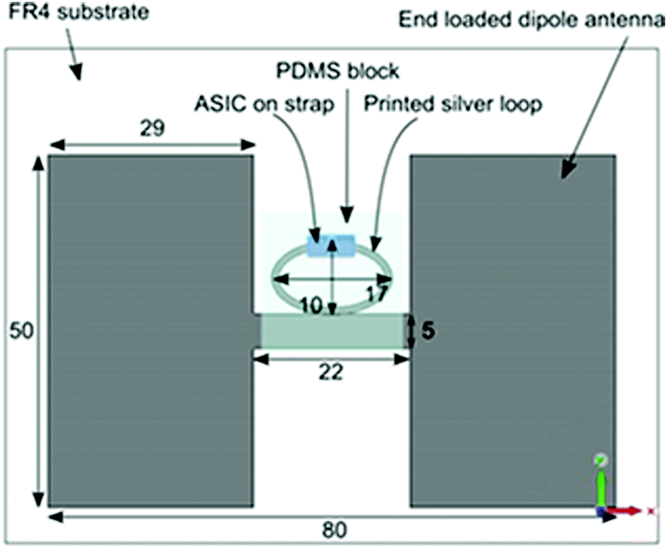 | ||
| Fig. 1 Schematic of antenna, PDMS substrate and printed silver loop which make up the RFID tag (all dimensions are in mm). | ||
2.5. RFID measurements
The ASIC chip was attached to the printed feed loop using an adhesive strip to give direct galvanic contact between the two terminals of the loop and the chip. The RFID tag was placed into a desiccator (internal seal diameter of 15.2 cm) with 50 cm3 of a chosen solvent. The desiccator was sealed with a flat glass lid. To assess the total achievable read range, the RFID reader antenna was placed at a calibrated distance of 30 cm below the tag. The achievable read range greater than 30 cm was then derived from measurement using a Voyantic Tagformance Lite RFID characterization system (Voyantic Ltd, Finland) which measures the backscattered power from the tag as a function of calibrated transmit power. The tag read range was measured with a Voyantic Tagformance life RFID characterization system (Voyantic Ltd, Finland) which measures the backscattered power for the tag as a function of calibrated transmitted power. Measurements were taken every two minutes over a period of up to 72 hours of solvent vapour exposure at 21 °C. For each measurement, the transmitted power from the reader was ramped from 0–26.5 dBm over the frequency range, 800–1000 MHz.2.6. Resistance measurements
A PDMS substrate with a printed loop was placed onto an FR4 board to hold it in place, whilst each terminal of the loop was put into contact with a test lead attached to a multimeter. This assembly was then placed inside a glass desiccator containing a saturated solvent vapour atmosphere. Resistance measurements were taken concurrently with the RFID measurements, and the substrate was removed from the vapour to allow contraction for the same length of time as those being used for RFID. Resistance measurements were recorded every minute, with initial measurements taken at 5 and 30 seconds on addition and removal of solvent vapour.3. Results and discussion
3.1. RFID sensor design
Antenna design for Ultra-High Frequency (UHF) RFID tags is highly dependent on the tuning of the tag antenna and transponder chip impedances. The impedance tuning, and hence the operation of the tag, is strongly influenced by the materials of which the tag is made and the electrical properties of its conductors.28,29 Should these parameters be altered then the power required from an external RFID system to activate the tag needs to be increased.30 Whilst in many situations the increased turn-on power is regarded as disadvantageous, it can also be turned to an advantage in that the varying power requirement can form the main mechanism for transmitting information from an environmental sensor. It is possible to account for variability in the wireless channel using signal processing algorithms.31The RFID sensor shown in Fig. 1 comprises four elements: (i) an antenna for RFID wireless communication, (ii) a sensing impedance transducer, (iii) a RFID integrated circuit (transponder chip), and (iv) a stimuli responsive polymer (PDMS). The antenna is tuned to the UHF RFID band, the transponder chip modulates information in the reflected signal, and the feed loop connects the antenna to the chip. In this passive RFID system, the tag is energized entirely by power provided from an external reader which in turn also receives the reflected tag signal. The purpose of the feed loop is to transform the impedance of the antenna so that it matches that of the transponder chip and ensures maximum power transfer between the two.28
Maximum power transfer between the feed loop and the transponder chip is essential to obtain the minimum amount of reader power required to activate the tag, and this is strongly affected by the conductivity of the loop and its exact position with respect to the dipole antenna.28 Therefore, a change in the electrical properties of the feed loop will cause the tag activation power to vary and this can be detected by the external reader. The majority of the tag surface area is covered by the antenna. The dipole width determines the bandwidth of operating frequencies while the end loading elements serve to reduce the overall tag length to below one half wavelength and make the tag more compact. In addition to the sensing capacity, the tag design should enable omni-directional radiation performance,32 with simple 2D manufacture whilst maintaining a relatively small antenna size.
Having defined the sensor antenna design, integration of the feed loop with the stimuli responsive polymer was necessary. PDMS swells in the presence of organic vapours and it was expected that either the expansion of the PDMS would disrupt the conductivity of the printed conducting loop track and/or that the dielectric properties of the PDMS substrate would change due to the presence of significant quantities of organic solvent bound in the PDMS. In either case the efficiency of the tag response would be altered and detected by an external reader because the level of transmitted power required to activate the sensing tag changes in proportion with the tag efficiency, which itself is a function of the exposure to the vapour stimulus. The increase in transmitted power required is reflected in a decrease in effective read range for the tag. The tag efficiency is defined as the amount of power radiated by the tag antenna divided by the power flowing at its terminals connecting to the transponder chip.
3.2. Inkjet printing
To enable the printing of the silver ink the PDMS was rendered hydrophilic by UV-ozone treatment following techniques reported in the literature. Fig. 2 shows the ATR-FTIR spectra of the PDMS before and after UV-ozone treatment. The appearance of the broad absorption around 3300 cm−1 and the absorption at 900 cm−1 demonstrated a large increase in the number of Si–OH bonds at the surface. After 24 hours the spectrum returned to its untreated state indicating the reorganization of the siloxane surface by the internalization of the polar Si–OH groups and the presentation of the Si–CH3 groups at the surface once more. Such behavior of polysiloxane surfaces has been well documented.33,34 With increased UV-ozone exposure times there is a predictable decrease in contact angle (Fig. 2 inset) followed by a recovery that never fully returns to its original value. Interestingly for long exposure times the recovery is quicker. The surface of the PDMS also becomes more brittle with longer exposure, with visible cracks appearing over the surface. In order to compensate for these effects a UV-ozone exposure time of 25 minutes was chosen for the preparation of PDMS used in the printing experiments. The contact angle for the silver ink after UV-ozone exposure was reduced to 34.0 ± 0.3°, a printed drop had a radius of approx. 50 μm (Fig. S2, ESI†) and patterns were readily obtainable.
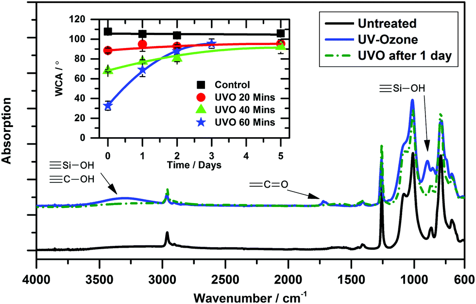 | ||
| Fig. 2 ATR-FTIR spectra for UV-ozone treated PDMS substrates. Blue (top) spectrum shows the appearance of OH stretching modes at approximately 3300 cm−1 and the subsequent loss after 1 day. Inset, shows the initial reduction in water contact angle (WCA) and subsequent recovery after UV-ozone treatment. | ||
Fig. 3 gives an overview of the findings of the optimization of printing silver ink onto the PDMS squares (see also Fig. S3, ESI†). Several clear trends were noticeable. Increasing the sintering temperature generally resulted in lower resistances with no significant improvement in performance discernible at temperatures higher than 150 °C (Fig. 3a and d). Increasing the number of layers of ink deposited (1, 2 or 3) led to decrease in resistance, corresponding to an increase in material and thickness of the printed line (Fig. S4, ESI†). Although a further increase in the number of layers printed could reduce the resistance further, factoring in material usage, cost and time led to the choice of a maximum of 3 layers for the creation of feed loops. Finally, drop spacing had a significant effect on the sheet resistance (Fig. 3b and e), with a smaller drop spacing giving a much improved performance. However, this had to be correlated with the quality of the printed pattern as demonstrated in Fig. S5 (ESI†). For drop spacings lower than 35 μm, bulges appeared in the printed lines for both 1 and 3 layers, increasing the average width of the line.
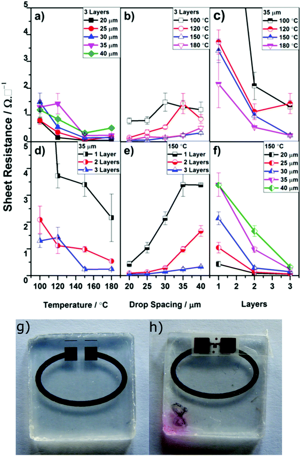 | ||
| Fig. 3 Optimization of printing colloidal silver inks on PDMS: sheet resistance for optimizing silver printing vs. temperature (a and d); drop spacing (b and e); number of layers (c and f); (g) the printed conductive feed loop; and (h) the feed loop with IC chip attached by adhesive strip. | ||
Combining these findings, feed loops were created using a drop spacing of 35 μm with three printed layers and a sintering temperature of 150 °C. Of a batch of 24 loops printed under these optimized conditions, 19 of them were seen to have resistances of less than 20 Ω and were considered suitable for incorporation into tags (Table S5, ESI†). Observations of buckling along the printed lines (Fig. S5, ESI†) is consistent with previous reports and is presumed to be due to expansion and contraction of the siloxane during the heating process, but was not seen to detrimentally affect RFID performance. Typical printed feed loops are shown in Fig. 3g and h.
3.3. RFID sensor response
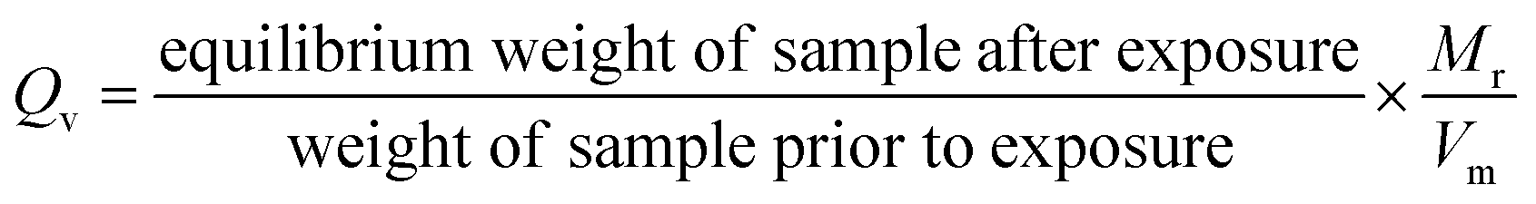
Previous work has demonstrated that the equilibrium swelling volume of a given PDMS sample in an organic vapour is as a function of the relative solubility of the organic solvent in PDMS and the vapour pressure.19 The compatibility of the PDMS with a given solvent could be modelled using the dispersive (δd), polar (δp) and hydrogen bonding (δh) contributions of the Hansen solubility parameter of both components in the function:| Ra = (4 × (δdsolvent − δdPDMS)2) + (δpsolvent − δpPDMS)2 + (δhsolvent − δhPDMS)2 | (1) |
| Qv = a + (bδd × δd) + (bδp × δp) + (bδh × δh) + (bVP × VP) | (2) |
 | (3) |
For the present study a number of solvents were chosen for testing based on their predicted ability to swell PDMS. Diethyl ether and dichloromethane swell PDMS very well, acetone and xylene moderately well, and methanol and propan-2-ol not at all. Additionally, we chose to test the sensors with ethyl acetate, acetaldehyde and acetic acid as representative food degradation products.35–38 The solubility parameters, vapour pressures, Ra values and predicted relative equilibrium swelling volumes of the test solvents are given in Table 1.
| Solvent | δ d | δ p | δ h | mmHg | R a | Predicted Qv |
|---|---|---|---|---|---|---|
| Acetaldehyde | 14.7 | 8 | 11.3 | 760.00 | 10.6 | 3.88 |
| Acetic acid | 14.5 | 8 | 13.5 | 15.53 | 12.2 | 1.31 |
| Acetone | 15.5 | 10.4 | 7 | 231.02 | 10.6 | 1.96 |
| DCM | 18.2 | 6.3 | 6.1 | 436.54 | 7.8 | 2.68 |
| Diethyl ether | 14.5 | 2.9 | 5.1 | 537.79 | 4.0 | 3.68 |
| Ethyl acetate | 15.8 | 5.3 | 7.2 | 94.51 | 5.8 | 1.81 |
| Methanol | 15.1 | 12.3 | 22.3 | 126.76 | 21.5 | 1.07 |
| Propan-2-ol | 15.8 | 6.1 | 16.4 | 45.15 | 13.2 | 1.34 |
| Xylene | 17.8 | 0.9 | 1.8 | 8.48 | 4.8 | 1.77 |
| PDMS | 15.9 | 0.1 | 4.7 | — | — | — |
The sensor tags were placed in a sealed glass vessel (a desiccator with flat glass plate lid) with an excess of the solvent in question at the base of the vessel. Transmitted power measurements were taken from the moment of enclosure. To measure recovery, the vessels were opened to the air and the tag removed from the saturated vapour environment.
Tags exposed to both diethyl ether, DCM, ethyl acetate and acetaldehyde vapours led to a rapid increase in required transmitted power reaching a maximum value in less than 5 minutes (Fig. 4a and Fig. S6–S8, ESI†). Accompanying the increase in transmitted power was a corresponding reduction in read range. Further, the recovery time after removal from the solvent vapour was typically less than 10 minutes. Remarkably, repeated cycles of exposure led to repeatable behavior in the tag response and a single tag could be exposed to vapour multiple times (Fig. 4b and Fig. S6–S11, ESI†) with the accompanying change in transmitted power and read range. In ‘average’ swelling solvents, such as acetone and xylene, the length of vapour exposure necessary to reduce the performance of the tag was longer (Fig. 4c and Fig. S9, ESI†). In contrast to the above results methanol, propan-2-ol and acetic acid solvents that do not swell PDMS appreciably gave essentially no response over extended periods of exposure (Fig. 4d and Fig. S10, S11, ESI†). The performance of the tags was seen to slowly decrease over much longer periods of time (up to 72 hours), but was not seen to cause enough disruption to stop the tag from responding entirely.
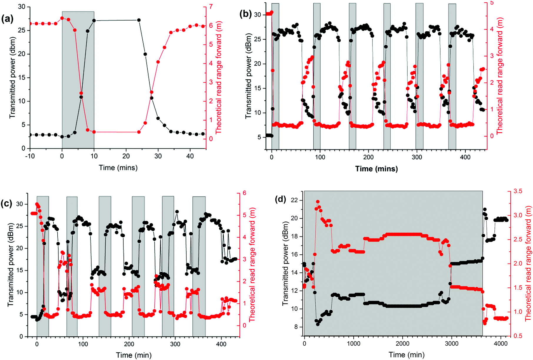 | ||
| Fig. 4 Transmitted power and forward read range measurements for an RFID tag exposed to representative vapours (the grey boxes indicate time that loop was exposed to vapour): (a) initial exposure to diethyl ether; (b) repeated exposures to diethyl ether; (c) repeated exposures to acetone; and (d) exposure to methanol. | ||
The change in the normalized response (based on a normalized scale of 100% before vapour exposure, Fig. S12 and S13, ESI†) as a factor of response time for each tag to reach minimum read range for the different vapours could be correlated with the predicted equilibrium swelling (Fig. 5). A strict comparison between relative response rates and predicted equilibrium swelling is not valid since the response rate will depend upon kinetic factors that are not part of the equilibrium swelling prediction model. The diffusion rates can vary considerably between vapours and this is particularly apparent for xylene which has been observed to show significantly lower diffusion rates in PDMS than other solvents. Thus while superficially the expected response for xylene should be similar to that of ethyl acetate a clear difference exists.
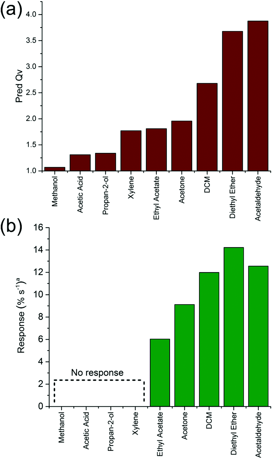 | ||
| Fig. 5 (a) Predicted equilibrium swelling values for PDMS in various solvent vapours and (b) measured response rates for tag response to vapours. | ||
There is a clear correlation between tag response and the properties of the solvent vapour the tag is exposed to, but it is also evident that the tag does not break after successive swelling cycles. As such, it became necessary to ascertain the mechanism by which these sensors were working.
3.4. Sensing mechanism
In the presence of solvent vapour the PDMS block properties such as form factor, electrical permittivity and surface properties can change. Changes in the antenna response can be caused by either structural changes of the metal or changes in the PDMS dielectric properties. Swelling will directly affect the printed conductor feed loop dimensions and/or the structural integrity of the feed loop causing the tag antenna to detune. Further, solvent absorption in the vicinity of the feed loop can adversely affect the feed loop electrical resistance and the matching of the antenna and chip impedances, consequently increasing the tag turn-on power and decreasing the read range.To monitor the changes in the feed loop on PDMS when exposed to vapour a tag was exposed to diethyl ether vapour and observed under a microscope. With increasing degree of vapour exposure it became obvious that the silver films constituting the loop cracked and fractured with the swelling of the PDMS substrate leading to increasing loss of contact between sections of the silver. This is best illustrated by the inverse images of a portion of loop before exposure, after 30 minutes exposure and then left to recover in air (Fig. 6, further microscope images are given in Fig. S14, ESI†). As can be seen gaps appear between ‘flakes’ of the silver with solvent exposure and these appear to rejoin as the vapour desorbs from the PDMS in air. Despite the ‘flakey’ appearance of the loops, the silver remained attached to the substrate during this process.
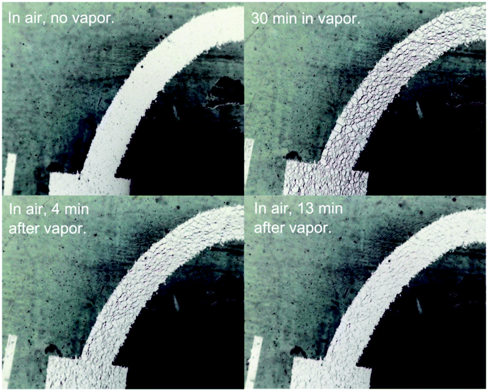 | ||
| Fig. 6 Inverse images of inkjet printed feed loop at various stages in the cycle of exposure to/removal of vapour: top left – before exposure; top right – after 30 minutes of vapour exposure; bottom left – 4 minutes after removal from vapour; and bottom right – 13 minutes after removal. Cracks can clearly be seen to form after vapour exposure, and loop to ‘reassemble’ after removal of vapour. | ||
Resistance values were taken in tandem with the RFID measurements with swelling and a direct correlation was observed between the two variables as shown in Fig. 7 (see also Fig. S15 and S16, ESI†). After a very short period in diethyl ether vapour, ca. 5 minutes, the resistance of the loop was seen to dramatically increase, until no reading could be obtained at all. This matched the length of time taken for the loop to require 26.5 dBm transmitted power in order to generate a response, which is the limit the RFID chip sensitivity. When the tags were removed from the solvent atmosphere, both the resistance and the required transmitted power were seen to decrease, as the PDMS contracted and the performance of the tag improved. The resistance initially decreased very rapidly, but then was observed to ‘tail off’, steadily returning to its original value. An RFID signal was consistently regained at approximately 24 Ω. Since variation in dielectric constant does not affect track resistance we can attribute the dominant sensing mechanism in these tags to the generation of cracks in the silver film during substrate expansion leading to increased resistance in the feed loop. This demonstrates that the response to swelling is not caused by any variation in the dielectric constant of the PDMS. Remarkably electrical contact is remade during the evaporation of the solvent and relaxation of the substrate.
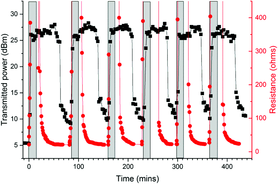 | ||
| Fig. 7 Transmitted power and resistance (measured concurrently) against time for an RFID tag in diethyl ether – the grey box indicates time that the loop was exposed to vapour. | ||
An increase in necessary transmitted power upon vapour exposure and a decrease in power after removal of the tag from the vapour continued through multiple cycles for all solvent vapours. Fig. 8 shows the maxima and minima transmitted power values for each solvent for each cycle. Whereas diethyl ether, ethyl acetate and acetaldehyde showed no significant degradation in performance acetone displayed a gradual reduction in necessary minimum power over 6 cycles and dichloromethane showed a noticeable reduction in performance after the 4th exposure cycle. The reasons for some degradation in performance for acetone and dichloromethane are currently unknown. As of yet the maximum number of cycles that these tags can undergo before failure or significant loss in sensitivity has not been tested. One of the applications initially envisaged for these sensors was in the area of food spoilage. Unfortunately the bulk of recent published research on spoilage has focused on the specific identification of volatile compounds indicators for electronic node type detectors rather than quantification of absolute amounts.42–44 However previous studies indicate that individual volatiles are produced in the 10s to 100s ppm (w/w or v/v) concentrations in the early stages of food spoilage; though given the large range of different foodstuffs, food lifetimes and degradation mechanisms these values can only be taken as indicative.45–47 However such concentrations of volatiles by themselves are too low to be detected by the current tag sensors described in this work. One approach to increase sensitivity will be to reduce the cross-link density of the polysiloxane matrix enabling larger degrees of swelling for smaller quantities of absorbed volatile. Secondly the absorption of a number of different volatiles simultaneously, will dramatically increase sensitivity; though the practicality of this will depend upon the foodstuff and packaging in question.
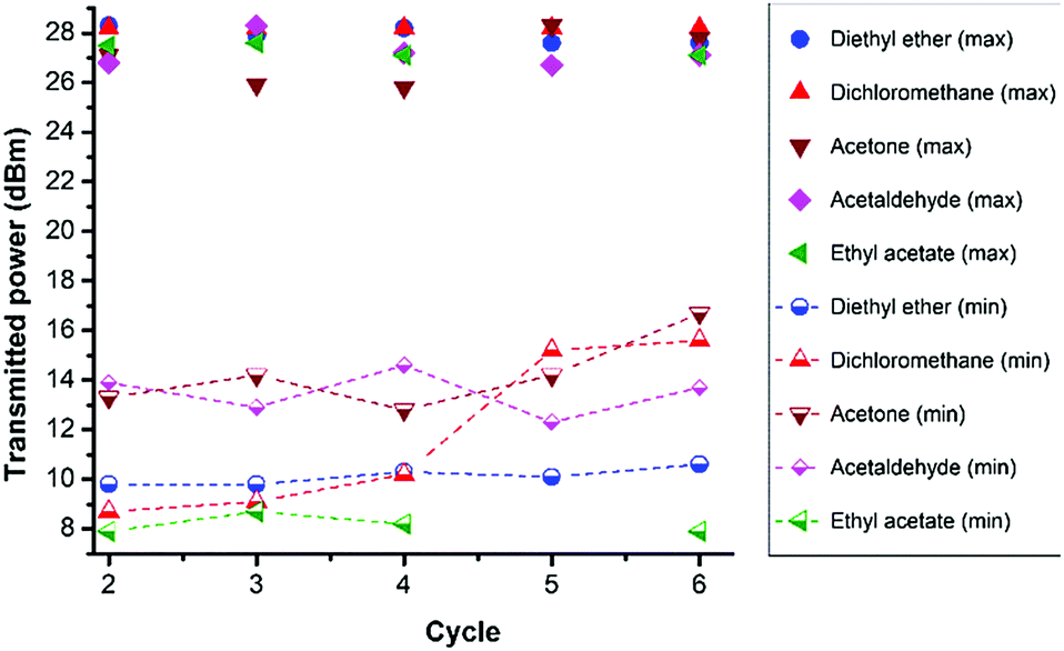 | ||
| Fig. 8 Maximum (max) and minimum (min) transmitted power perc cycle for reach solvent. | ||
4. Conclusion
We have demonstrated that we can print colloidal silver ink solutions using inkjet technology onto pre-molded PDMS substrates, and thermally sinter them to give conductive loops. By optimizing the printing conditions, loops with resistances of below 20 Ω can be produced. With an end loaded dipole antenna, this produces a vapour sensitive RFID tag.These tags are shown to swell when placed in a solvent vapour atmosphere, which results in a dramatic increase in resistance across the printed loop. This corresponds to a significantly decreased (and ultimately, eradicated) read range, with a much higher transmitted power required to receive a response from the tag. Results from this study suggest that the large increase in resistance with swelling is a direct consequence of the fracturing/cracking of the printed silver loop that accompanies the swelling of the PDMS.
The reversibility of this solvent detection is demonstrated by the tag recovering from the loss of read range and increased transmitted power, returning to a working RFID tag after a period of time away from solvent vapour. The length of time taken for the tag to stop responding, and to return to life again, is highly dependent on the organic vapour that it is being exposed to. This selectivity will be further improved by the addition of functional groups to the siloxane network. This system could be used for numerous applications, such as the detection of food spoiling both on a small scale (in consumer's homes) and on a much larger scale (degradation of food during processing and transport). Further work is being carried out to enable this system to be made entirely by additive manufacturing.
Acknowledgements
We wish to thank the EPSRC for funding this project (EP/L019868/1 and EP/L019728/1).Notes and references
- G. Marrocco, IEEE Wireless Commun., 2010, 17, 10–17 CrossRef.
- C. Occhiuzzi, S. Caizzone and G. Marrocco, Europe, 2013, 866, 3.2 Search PubMed.
- R. A. Potyrailo, N. Nagraj, Z. Tang, F. J. Mondello, C. Surman and W. Morris, J. Agric. Food Chem., 2012, 60, 8535–8543 CrossRef CAS PubMed.
- R. A. Potyrailo, W. G. Morris, T. Sivavec, H. W. Tomlinson, S. Klensmeden and K. Lindh, Wireless Commun. Mobile Comput., 2009, 9, 1318–1330 CrossRef.
- E. M. Amin, J. K. Saha and N. C. Karmakar, IEEE Sens. J., 2014, 14, 2198–2207 CrossRef.
- Y. Feng, L. Xie, Q. Chen and L.-R. Zheng, IEEE Sens. J., 2015, 15, 3201–3208 CrossRef.
- J. Gao, J. Sidén, H.-E. Nilsson and M. Gulliksson, IEEE Sens. J., 2013, 13, 1824–1834 CrossRef CAS.
- S. Manzari, C. Occhiuzzi, S. Nawale, A. Catini, C. Di Natale and G. Marrocco, IEEE Sens. J., 2012, 12, 2851–2858 CrossRef CAS.
- A. Oprea, J. Courbat, N. Bârsan, D. Briand, N. De Rooij and U. Weimar, Sens. Actuators, B, 2009, 140, 227–232 CrossRef CAS.
- A. Oprea, N. Bârsan, U. Weimar, M.-L. Bauersfeld, D. Ebling and J. Wöllenstein, Sens. Actuators, B, 2008, 132, 404–410 CrossRef CAS.
- Y. Jia, M. Heiß, Q. Fu and N. A. Gay, Education Technology and Training, 2008 and 2008 International Workshop on Geoscience and Remote Sensing. ETT and GRS 2008. International Workshop on (vol. 2, pp. 496–499), IEEE, 2008.
- R. A. Potyrailo, C. Surman, W. G. Morris, S. Go, Y. Lee, J. Cella and K. S. Chichak, IEEE International Conference on RFID, IEEE RFID, 2010, 2.
- R. Potyrailo, C. Surman, W. Morris and S. Go, Proc. Transducers ′09, 2009, 1650.
- R. A. Potyrailo, C. Surman, S. Go, Y. Lee, T. Sivavec and W. G. Morris, J. Appl. Phys., 2009, 106, 124902 CrossRef.
- R. A. Potyrailo, A. Burns, C. Surman, D. J. Lee and E. McGinniss, Analyst, 2012, 137, 2777–2781 RSC.
- L. K. Fiddes and N. Yan, Sens. Actuators, B, 2013, 186, 817–823 CrossRef CAS.
- C. Occhiuzzi, S. Caizzone and G. Marrocco, IEEE Trans. Antennas Propag., 2013, 55, 14–34 CrossRef.
- J. N. Lee, C. Park and G. M. Whitesides, Anal. Chem., 2003, 75, 6544–6554 CrossRef CAS PubMed.
- C. Rumens, M. A. Ziai, K. Belsey, J. C. Batchelor and S. J. Holder, J. Mater. Chem. C, 2015, 3, 10091–10098 RSC.
- H.-H. Lee, K.-S. Chou and K.-C. Huang, Nanotechnology, 2005, 16, 2436 CrossRef CAS PubMed.
- J. Perelaer, A. W. de Laat, C. E. Hendriks and U. S. Schubert, J. Mater. Chem., 2008, 18, 3209–3215 RSC.
- J. Perelaer, C. E. Hendriks, A. W. de Laat and U. S. Schubert, Nanotechnology, 2009, 20, 165303 CrossRef PubMed.
- A. Kamyshny, J. Steinke and S. Magdassi, Open Appl. Phys. J., 2011, 4, 19 CrossRef CAS.
- K. Efimenko, W. E. Wallace and J. Genzer, J. Colloid Interface Sci., 2002, 254, 306–315 CrossRef CAS PubMed.
- H. T. Kim and O. C. Jeong, Microelectron. Eng., 2011, 88, 2281–2285 CrossRef CAS.
- S. Chung, J. Lee, H. Song, S. Kim, J. Jeong and Y. Hong, Appl. Phys. Lett., 2011, 98, 153110 CrossRef.
- Y. Kim, X. Ren, J. Kim and H. Noh, J. Micromech. Microeng., 2014, 24, 115010 CrossRef.
- K. S. Rao, P. V. Nikitin and S. F. Lam, Proceedings of the 4th IEEE Workshop on Automatic Identification Advanced Technologies, 2005, 39–42.
- K. S. Rao, P. V. Nikitin and S. F. Lam, IEEE Trans. Antennas Propag., 2005, 53, 3870–3876 CrossRef.
- D. M. Dobkin and S. M. Weigand, Microwave Symp. Dig., 2005, 12, 4 Search PubMed.
- E. Abad, F. Palacio, M. Nuin, A. G. De Zarate, A. Juarros, J. Gómez and S. Marco, J. Food Eng., 2009, 93, 394–399 CrossRef.
- X. Qing and N. Yang, IEEE Antennas Propag. Soc. Int. Symp., Dig., 2004, 97–100 Search PubMed.
- J. A. Crowe, K. Efimenko and J. Genzer, in Science and Technology of Silicones andSilicone-Modified Materials, ed. S. J. Clarson, J. J. Fitzgerald, M. J. Owen, S. D. Smith and M. E. Van Dyke, American Chemical Society, 2007, vol. 16, pp. 222–255 Search PubMed.
- J. E. Mark, Acc. Chem. Res., 2004, 37, 946–953 CrossRef CAS PubMed.
- L. Freeman, G. Silverman, P. Angelini, C. Merritt and W. Esselen, Appl. Environ. Microbiol., 1976, 32, 222–231 CAS.
- C. D. Man and A. A. Jones, Shelf Life Evaluation of Foods, Springer, 1994 Search PubMed.
- R. Pierami and K. Stevenson, J. Dairy Sci., 1976, 59, 1010–1015 CrossRef CAS.
- R. L. Wierda, G. Fletcher, L. Xu and J.-P. Dufour, J. Agric. Food Chem., 2006, 54, 8480–8490 CrossRef CAS PubMed.
- C. M. Hansen, Hansen Solubility Parameters: A User's Handbook, CRC press, 2007 Search PubMed.
- D. R. Lide, Handbook of Organic Solvents, CRC Press, 1994 Search PubMed.
- D. R. Lide and H. V. Kehiaian, CRC Handbook of Thermophysical and Thermochemical Data, CRC Press, 1994 Search PubMed.
- J. M. Cevallos-Cevallos, J. I. Reyes-De-Corcuera, E. Etxeberria, M. D. Danyluk and G. E. Rodrick, Trends Food Sci. Technol., 2009, 20, 557–566 CrossRef CAS.
- I. A. Casalinuovo, D. Di Pierro, M. Coletta and P. Di Francesco, Sensors, 2006, 6, 1428–1439 CrossRef.
- A. Önal, Food Chem., 2007, 103, 1475–1486 CrossRef.
- Z. Karpas, B. Tilman, R. Gdalevsky and A. Lorber, Anal. Chim. Acta, 2002, 463, 155–163 CrossRef CAS.
- G. López-Gálvez, G. Peiser, X. Nie and M. Cantwell, Z. Lebensm.-Unters. -Forsch. A, 1997, 205, 64–72 CrossRef.
- J. Schnürer, J. Olsson and T. Börjesson, Fungal Genet. Biol., 1999, 27, 209–217 CrossRef PubMed.
Footnote |
| † Electronic supplementary information (ESI) available. See DOI: 10.1039/c6tc05509e |
| This journal is © The Royal Society of Chemistry 2017 |