
 Open Access Article
 This Open Access Article is licensed under a
 Creative Commons Attribution 3.0 Unported Licence
Flash spark plasma sintering of magnesium silicide stannide with improved thermoelectric properties
Baoli
Du
 *ab,
Francesco
Gucci
b,
Harshit
Porwal
b,
Salvatore
Grasso
b,
Amit
Mahajan
b and
Mike J.
Reece
*b
*ab,
Francesco
Gucci
b,
Harshit
Porwal
b,
Salvatore
Grasso
b,
Amit
Mahajan
b and
Mike J.
Reece
*b
aSchool of Physics and Chemistry, Henan Polytechnic University, Jiaozuo 454000, China. E-mail: dbl@hpu.edu.cn
bSchool of Engineering and Materials Science, Queen Mary University of London, London E1 4NS, UK. E-mail: m.j.reece@qmul.ac.uk
First published on 19th January 2017
Abstract
Spark plasma sintering has become a routine method for the densification of thermoelectric (TE) materials. However, the impacts and details of direct Joule heating within TE materials have not been fully quantified and clarified. Here we investigated the feasibility of flash-sintering (high heating rate Joule heating) magnesium silicide stannide (MSS) using a spark plasma sintering furnace. A Mg2.1Si0.487Sn0.5Sb0.013 (MSS) green compact was sandwiched between two graphite punches without a die. Then a DC pulse voltage was applied between the punches and the current passed completely though the compact, without any of the current bypassing through a graphite die as occurs with a convectional SPS die–punch system. The direct heating was so efficient that a heating rate of ∼1000 °C was achieved and the sample was fully sintered in less than 45 s. Due to the high local Joule heating at the contacts of the particles, the MgO distribution pattern was modified and optimised, which broke the coated passivation layer on the MSS aggregates. The onset densification temperature was 170 to 350 °C lower than that in convectional SPS (750 °C). Importantly, it was possible to produce dense samples in a wide sintering window of ∼6 s, and the flash-sintering was controllable and repeatable. Flash sintering could open a new way for rapid densification of dense nanostructured and/or textured TE materials with low electrical resistivity by optimising the distribution or removal of the surface oxidation of the powder grains.
Introduction
Thermoelectric (TE) conversion technology has the potential to contribute to alleviating the global sustainable energy crisis and significantly reducing fuel consumption, and CO2 emissions. It is capable of recovering energy from a vehicle's exhaust and industrial waste heat whenever a temperature gradient is available.1–3 The efficiency of a TE material is described by a figure-of-merit ZT. Z is the square of the Seebeck coefficient, divided by the product of the electrical resistivity and thermal conductivity, and T is the absolute temperature.4The most successful commercial TE materials are based on bismuth telluride and its solid solutions. They are prepared by directional solidification from melt followed by a zone melt technique, which is capable of producing preferred orientation of the crystal grains, but it is rather time- and energy-consuming.4 The use of telluride compounds is limited by the toxicity and rarity of tellurium, and it also has the additional disadvantage of resource competition with cadmium telluride thin-films for solar cell application5 and phase change memory chips.6 Though single-crystal growth routes, including directed crystallization, Czochralski,7 floating zone,8 self-flux9 and vertical Bridgman technologies10 are still in use to produce magnesium group IV compounds, silicides, clathrates and chalcogenides, most of the newly developed TE materials are produced using a typical two-step route, powder synthesis followed by a densification process.
Powder metallurgy is a commonly used densification route in industry and is capable of handling large amounts of powder.11,12 But the lower density and porosity it achieves compared to melt processing would further deteriorate the notoriously brittle mechanical behaviour of TE materials, which are mainly formed by weak covalent or van der Waals bonding.13 Another route is the thermal and pressure assisted hot-pressing method.14 The sample is heated from outside to inside by thermal conduction through the die/punch system, which is heated by resistance or induction heating. Due to the nature of the indirect heating, the ramp rate is limited and the holding time is in minutes to hours, which is helpful to achieve uniform bulk materials, but makes it difficult to maintain precise control of the volatile components and avoid grain coarsening.15
In the last ten years, electric current assisted sintering technology (ECAS, also known as FAST),16–18 especially spark plasma sintering (SPS) and pulse activated sintering, are the most popular routes to achieve high performance materials from nanopowders. SPS inherited the same graphite die/punch assembly as used in hot-pressing. The design of direct current heating has increased the ramp rate and shortened the holding time, which is vital to maintain the fine microstructure of the starting powder to the sintered material.19 However, the portion of current passing through the powder is strongly dependent on the relative resistance of the powder compact and the graphite dies system.20,21 For a high resistance powder, most of the current passes through the conductive die and there is little direct current Joule heating of the sample. For TE materials with moderate resistivity, the sintering is partly assisted by the direct Joule heating produced by the portion of the current passing through the powder. So the sintering can be regarded as a hybrid of direct Joule heating assisted sintering and hot pressing. However, the impacts of direct Joule heating within the medium resistance TE materials were not fully demonstrated and clarified.
Recently, flash sintering at critical combinations of temperatures and applied electric fields has been demonstrated to sinter nanograin sized zirconia in less than 5 s at 850 °C, which conventionally needs several hours of processing in a conventional furnace at 1450 °C. The local Joule heating at grain boundaries not only facilitates grain boundary diffusion but also restricts grain growth.22,23
Taking into account of the much lower electrical resistance of TE materials compared to zirconia and its lower conventional SPS sintering temperature, it should be possible to flash sintering them in an SPS furnace, as has already been demonstrated for ZrB2,24 SiC,25 B4C,26 Nd–Fe–B27 and, 3YSZ28 where heating rates of >8000 °C min−1 were achieved.
Aiming to extend the applicability of flash sintering to TE materials and clarity the influences of direct Joule heating, magnesium silicide stannide (MSS) solid solution was chosen to investigate the effect of electric flash sintering on the microstructure, phase structure, surface oxidation removal and TE properties. We designed a flash sintering configuration that does not require the preheating and high voltage critical to flash sinter zirconia. Moreover, we aimed to run the flash sintering smoothly in a controllable way without an exponential increase of current at a critical point. MSS is suitable to harvest energy in the temperature range of 100–500 °C. Sb doped MSS has a figure-of-merit (ZT) larger than unity and exhibits good mechanical stability.29–31 However, fine MSS powder reacts with moisture and oxygen in air and forms a passivating oxidized layer on the surface of the particles. The composition around Si/Sn = 1 has a tendency to segregate into Sn-rich and Si-rich phases because of the miscibility gap in the Mg2Si and Mg2Sn pseudo-binary phase diagram.32–34 This means that the microscopic composition distribution is very sensitive to local temperature fluctuations and gradients that might be created by local Joule heating in flash sintering. So MSS is an ideal candidate to study the influence of flash sintering on TE materials, including possible particle surface cleaning or oxidation layer removal effects.
Experimental details
A SPS furnace (FCT HPD 25; FCT Systeme GmbH, Rauenstein, Germany) was used for the flash sintering studies. First MSS Mg2.1Si0.487Sn0.5Sb0.013 green compacts (∅20, height 2.5 mm) were obtained by partial sintering in a conventional die/punch system in the SPS at a fixed ramp rate of 100 °C min−1 under the minimum applied force (5 KN) until they reached the target relative density/shrinkage, at which point it was stopped manually. It was necessary to partially sinter the samples so that they had sufficient strength to sustain the minimum applied force (5 KN) applied by the SPS furnace to achieve good electrical contact. An alternative way to achieve this could be to cold press the powder with some binders.In order to clarify the effect of flash sintering on oxygen distribution, the MSS powder was exposed to dry air for 12 months to form a saturated oxidation layer. Then the green compact was sandwiched between two graphite punches under the minimum applied force without a die and inserted in between the pistons of the SPS furnace. Ductile multilayer insulating alumina paper rings were placed around the green compact to minimize the heat loss and temperature gradient along the radial direction as shown in Fig. 1 (inset). To reduce thermal conduction between the green compact and the SPS pistons, a double layer of electrically conducting graphite paper discs and a single layer of graphite felt disk were placed between them. All the auxiliary components, including alumina paper and graphite felt, were used as thermal insulating or buffer layers. No die or conductive wrapping were employed as auxiliary heating sources. So all of the applied current passed through the green compact. The samples sintered using this method are referred to as FSPS.
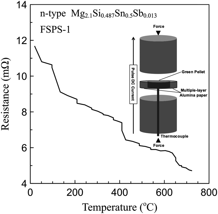 | ||
| Fig. 1 Schematic diagram of flash sintering in a spark plasma sintering furnace (inset), and temperature dependence of resistance of the green compact for FSPS-1 sample during flash sintering. | ||
To achieve flash sintering, the green compact needs to have a suitable electrical resistance in the whole processing temperature range to hold a sufficient voltage drop (electric field gradient) and current simultaneously to achieve the necessary direct Joule heating. Too conductive would result in the voltage drop (heating) occurring mainly on the SPS internal circuit rather than the green compact. Too high a resistance would minimize the current flow while maximizing the electric field gradient, which may lead to instability when the field is greater than a threshold value.22 Also, the power dissipation in the sample would be too low to achieve the required temperature.
All of the experiments were performed in a vacuum of ∼7 Pa. The temperature was monitored using a 1 mm diameter K-type thermocouple in direct contact with the bottom surface of the sample. The response time of thermocouple is less than one second, so the error of the temperature measurement is less than 20 °C when the ramp rate is ∼1000 °C min−1. During sintering, all of the parameters (i.e. processing time, temperature, voltage, current, and piston travel distance and speed) were monitored and logged.
Characterisation
The constituent phases of the samples were characterized using powder X-ray diffraction (XRD, X'Pert PRO-PANalytical, CuKα) in the 2θ range 5–120°. The microstructures of the samples were studied using a scanning electron microscope (SEM, FEI Inspect TM-F) in back scattered mode with combined energy dispersive X-ray spectroscopy (EDS). The topography and conductivity profiles were determined simultaneously using NT-MDT machine in conducting Atomic Force Microscopy (C-AFM) mode. The measurements were carried out using a soft Pt-coated cantilever with spring constant of 5.4–16 N m−1 and resonance frequency of 150–300 kHz (MikroMasch HQ:NSC35/Pt). The conducting profiles were obtained on polished samples with the application of 5 V voltage and setting the current to ∼10 nA. Electrical resistivity and Seebeck coefficient were measured by a commercial instrument (ZEM-3, Ulvac, Inc.) in a He atmosphere. Thermal conductivity was determined from thermal diffusivity data measured using the laser-flash method in a flowing Ar atmosphere (LFA-457, Netzsch), the specific heat capacity, and the density. The specific heat capacity of the materials was measured by power compensation differential scanning calorimetry (DSC, TA, Q20), and the data saturated at the Dulong–Petit value above 400 K. However, due to the complex phase structure and microstructure, the data fluctuated around the high temperature limit. This phenomenon has also been reported in the literature.35 So the Dulong–Petit value was used to calculate the thermal conductivity.Results and discussion
Sintering curves
The voltage, current, piston travel (sample shrinkage) and temperature during flash sintering are plotted in Fig. 2. The starting time of the processing was off-set to zero second to facilitate the discussion. To maintain a roughly constant ramp rate of about 1000 °C min−1, a three-stage sintering profile was used with power input steps of 40%, 45% and 55%. Because of the moderate and smoothly decreasing resistance of the green compacts during heating (Fig. 1), the current and voltage increased steadily in each stage without a dramatic increase above a critical temperature, as occurs in flash sintering of ceramics.22 The sintering was started from room temperature (no furnace preheating) with a power input of 40% for 5 s. Then the power was increased to 45% until 400 °C (about 15 s). Finally, the duration of the last stage with power input of 55% was used to achieve the final sintering temperature. We used the FSPS-1 sample to determine the duration of the third stage (or final temperature) and found an abrupt increase in piston travel at 42 s (25 s in the third stage), which indicated the melting of the green compact. More importantly, the piston travel showed a plateau between the 36th and 42nd second, which indicated a 6 s sintering window for the green compact. A fully dense pellet was achieved whenever the sintering process was stopped in this range, and the rapid flash sintering was controllable and repeatable. Another two samples were sintered following the above processing schedule and manually stopped at the start of the sintering window (36th second) for the FSPS-2 sample, and at the middle point of the window (40th second) for the FSPS-3 sample. Both samples were fully dense. So it is feasible to prepare bulk MSS material from green compact in less than 45 s with a heating rate of 1000 °C min−1 by flash sintering without preheating and die.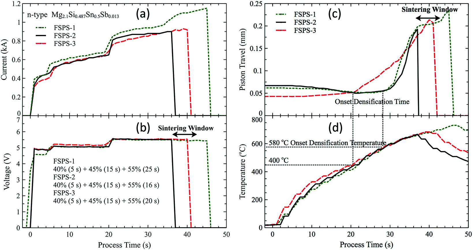 | ||
| Fig. 2 (a) Applied voltage, (b) current, (c) piston travel (shrinkage) and (d) temperature achieved during flash sintering for samples FSPS-1, FSPS-2 and FSPS-3. | ||
For comparison, MSS powder was sintered using a conventional SPS set up with a die–punch system with a heating rate of 100 °C min−1, and holding at 750 °C under a force of 5 KN for 1 min (same sample size used for FSPS, ∅20, height 2.5 mm). The pressure was then increased to 16 KN to complete the densification of the sample. These processing conditions were based on the optimized processing conditions used in previous work.31 Two different conventionally spark plasma sintered samples were prepared, one using the same type of green compact sample used for the flash sintering and the other using the starting powder, and referred to as CSPS-GC and CSPS-powder, respectively. The SPS parameters, including applied force/heating power, temperature and piston travel are shown in Fig. 3. Both the CSPS-GC and CSPS-powder samples did not show any shrinkage before reaching 750 °C under the same force of 5 KN as used in the FSPS processing. However, the FSPS samples started to densify at 580 °C for FSPS-1 and FSPS-2, and an even lower temperature of 400 °C for FSPS-3 sample. This suggests that flash sintering is capable of decreasing the onset densification temperature for MSS from 750 °C to <580 °C. During flash sintering, a large proportion of voltage drop occurs at the high resistance grain contacts within the grain boundary oxide layer of the powders. The extremely rapid Joule heating that occurred at the grain contacting necks facilitated the rearrangement of the grains, and the creation of thermally activated point defects, which in turn lowered the threshold energy for the relative motion of the grains and resulted in the densification of the green compacts at lower temperatures.36 In extreme circumstances, microscale local melting can occur at the grain contacts and lubricate the relative motion, and accelerate the re-arrangement and net formation of the grains.
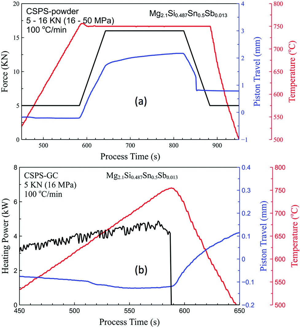 | ||
| Fig. 3 Applied force/heating power, piston travel and temperature achieved during conventional spark plasma sintering for (a) CSPS-powder and (b) CSPS-GC samples. | ||
Phase structure analysis
The samples prepared using the three different processing routes exhibited completely different phase structures. As shown in Fig. 4, the original powder is a MSS solid solution with small amounts of MgO. The CSPS-powder sample nearly maintained the same phase structure after holding at 750 °C for 5 min. However, the CSPS-GC sample separated into tin-rich and tin-poor MSS solutions. This is the typical reaction for MSS solid solutions with composition within the miscibility gap after heat treatment below the spinodal lines.34 During the flash sintering process, the local Joule heating created large temperature fluctuations and gradients from the center of the grains to their surface. Part of the corner and/or shell of the grains were locally melted and squashed into the pores between the grains. While cooling down, the melt solidified and separated into tin-rich and tin-poor phases. Together with the inner phase of the grains, the FSPS sample was a composite with three isostructural phases. The severe phase segregation perfectly demonstrates the effects of the local Joule heating in flash sintering. It is a powerful tool to fast sintering fine powders at low densification temperatures, while maintaining the fine microstructure in the bulk materials, and thus lowering the lattice thermal conductivity. The local melt produced lubrication for the relative motion of the grains, and it is possible to prepare samples with anisotropic microstructure and properties whenever the grains can be aligned under SPS uniaxial pressure. To keep the integrity of the sample, grain alignment usually happens at comparatively high temperatures when the sample is a little bit ‘soft’ due to the formation of a liquid phase due to melting. Under flash sintering conditions, part of the ‘necks’ joining adjoining grains melt due to the strong local Joule heating, which facilitates the relative motion of the adjoining particles. This means that the alignment of the grains may happen at lower temperatures and pressures compared with conventional sintering. Also, in the presence of a liquid phase at grain boundaries, we do not need to worry about the integrity of the compact because the melt phase can join the grains together on cooling down. In this work, the composition of the powder is in the miscibility gap of the pseudo-binary Mg2Si–Mg2Sn phase diagram, which resulted in phase segregation after cooling. This well demonstrated the presence of the local melting by strong local Joule heating.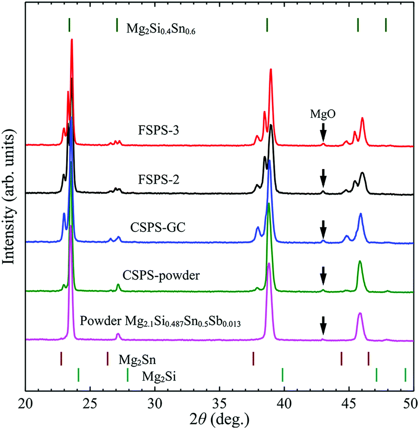 | ||
| Fig. 4 XRD patterns for original powder, CSPS-powder, CSPS-GC, FSPS-2 and FSPS-3 samples. | ||
Microstructure and composition analysis
Fig. 5(a) shows a typical back scattered image of the CSPS-powder sample. The black dots corresponded to MgO impurity, which wraps around the MSS grains. Due to the agglomeration of the MSS powder, the oxide layer formed mostly on the surface of the aggregates and the internal grains were quite free of oxidation. Benefiting from the homogeneous heating with the help of a conductive die during the conventional SPS processing route, there was no liquid phase generated up to the maximum processing temperature and the oxide distribution in the bulk material was at the boundaries of the original aggregates. Although MSS is prone to segregation at the microscale during the heating process, the holding at 750 °C (above spinodal phase boundaries) promoted the formation of a single solid solution phase.34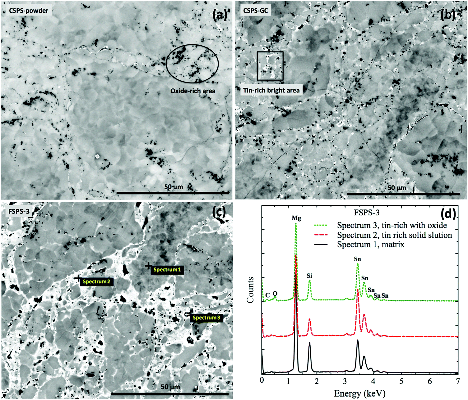 | ||
| Fig. 5 Back-scattering images for (a) CSPS-powder, (b) CSPS-GC and (c) FSPS-3 samples with (d) EDS results. | ||
Mild phase segregation was observed in the CSPS-GC sample (Fig. 5(b)), which had experienced two cycles of heat treatments up to 750 °C without a holding time. Unlike the crack-free CSPS-powder sample, CSPS-GC sample was highly microcracked. We related this phenomenon to the violent expansion of the green compact during the heating process, which generated high thermal stresses that damaged the rigid connection between adjoining grains, and thus the integrity of the green compact.
Segregation of several phases occurred in the FSPS samples (Fig. 5(c)), which is consistent with their complex phase structures. High local Joule heating produced melting at the grain contacts, which was pressed into and filled the voids and pores in between the grains. The local melting phase released the thermal strain within the green compact by allowing the grains to rotate/move more easily, which helped the samples to maintain their integrity. Therefore, much less cracking was observed in the FSPS samples. These results indicate that high local heating/melting is vital to the integrity of the sample during sintering from green compact. At least, part of the surface oxide at grain contacts was wrapped in the tin-rich melt and squashed into the voids and pores between the high melting point tin-poor grains. The melting phase re-joined the adjoining grains together, creating an oxide-free network for the flow of charge carriers. This feature is demonstrated in the EDS composition analysis shown in Fig. 5(d). Spectrum 2, which was collected from a bright area, was rich in tin compared with Spectrum 1 from a dark area. The tin-rich component formed a network around the matrix and wrapped most of the oxide within it (Spectrum 3). The re-distribution of the MgO surface coating around the original agglomerates facilitated the flow of charge carriers.
Topography and conducting profiles analysis
AFM topography and conductivity imaging revealed more details of the distribution of the MgO. Fig. 6 shows topographic and conductivity images of the FSPS-3 sample. The bright regions in the conductivity image correspond to regions of high conductivity. The topographic image shows that the polished surface does not have apparent height contrast except for protrusion of bright dots/lines/areas (BDLAs). The BDLAs correspond to dark areas with lowest conductivity in the corresponding conductivity image. So, they were identified as high-resistance MgO.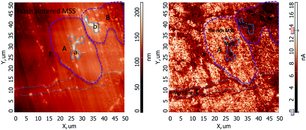 | ||
| Fig. 6 (left) Topography and (right) conducting profile of flash sintered FSPS-3 sample. The dotted lines, and solid and dashed encircled areas were drawn to guide the reader's eyes. | ||
To better identify the MgO distribution, dotted lines have been drawn in Fig. 6 to guide the readers' eyes to identify the lines of MgO grains. In most cases, the areas on either sides of the dotted lines do not have apparent contrast in the conductivity image, except for the homogeneous background patterns created by electronic noise. This indicates that the MgO lines were wrapped by regions of tin-rich composition, which are identified by the brighter areas in the conductivity image. Possibly, the wrapping distribution of MgO in the tin-rich composition modified the path for the charge carriers, making the material more electrically conductive. The linear distribution patterns shared lots of similarity with the MgO patterns observed in the back scattered image. As shown in Fig. 5(c), most of the MgO impurities were wrapped in the tin-rich areas and the tin-poor areas seemed to be left rather oxygen-free. This pattern also existed along the grain boundaries in the CSPS-powder sample (Fig. 5(a)), where it was inherited from the surface passivated powder and produced a negative influence on the charge carrier transportation.
Large MgO areas, for example, areas ‘a’ and ‘b’, in the topographic and conductivity images have been marked by solid lines. Their surrounding areas labeled as ‘A’ and ‘B’, exhibit high conductivity and low conductivity in the conductivity image, respectively, while they do not have much contrast in the topographic image. Due to the resolution limit and the low working voltage (maximum 10 V) of the AFM, the mapping image does not show apparent contrast between MgO and the high resistance tin-poor composition. However, combining the phase structure and the SEM results, we identified that area ‘B’ is a relatively high resistance tin-poor MSS, rather than MgO. This means that MgO areas were wrapped in or next to both high conductivity tin-rich (A) and high resistivity tin-poor (B) compositions. This character did not disclose itself in backscattered images. The above discussion suggests that the FSPS sample had more enriched MgO distribution patterns in MSS than the samples prepared using conventional SPS. Keeping in mind that any modification of the MgO distribution pattern may break the coated passivation layer on MSS aggregates, we conjecture that the FSPS process facilitates the flow of charge carriers, which would explain the much lower resistivity of the FSPS material reported in the next section.
Thermoelectric properties
The TE parameters, including resistivity, Seebeck coefficient, thermal conductivity and figure-of-merit ZT of the CSPS-powder, FSPS-2 and FSPS-3 samples are shown in Fig. 7. The CSPS-GC sample, which was highly cracked, is not included for comparison. The CSPS-powder sample showed much higher resistivity than the historical results for a similar material prepared using a powder with similar composition (free of surface oxidation) processed in a similar way.31 This suggests that the oxide surface layer on grains effectively blocked the flow of charge carriers even in a fully dense sample. The FSPS samples have a more than four times lower resistivity than the CSPS-powder sample. The re-distribution and possible electrochemical reduction of the surface oxide layer during FSPS created a charge carrier highway network through the sintered material. Although the FSPS sample had a lower absolute Seebeck coefficient, its power factor was much higher than that of the CSPS-powder sample. All of the samples have similar and rather low thermal conductivity ∼1.5 W m−1 K−1 compared with pure magnesium silicide (∼7 W m−1 K−1) or stannide (∼10 W m−1 K−1).37 Upon heating, thermal conductivity first decreases and then rapidly increases at high temperatures. The rapid increase beyond 300 °C is attributed to an enhancement of ambipolar thermal conductivity aroused from the intrinsic excitation.31,35 The FSPS samples have higher thermal conductivities than CSPS-powder sample. In general, the low sintering temperature in flash sintering is effective in restraining the coarsening of the grains and maintaining the fine microstructure of the staring powder in the sintered compact, and thus decreasing thermal conductivity. However, due to the formation of the tin-rich phase network in the FSPS samples, their thermal conductivity increased compared to the CSPS samples. This is mainly related to the specifically chosen compositions within the miscibility gap of the pseudo-binary Mg2Si–Mg2Sn phase diagram. A ZT of 0.7 was achieved at 400 °C for the FSPS samples. Though this value is not very impressive compared with samples prepared by a conventional route,29,31 the above result demonstrates the strong effects of flash sintering on phase structure, microstructure, and surface oxide layer removal. By taking advantage of the good electrical conductivity of TE materials, flash sintering could open a new way for the rapid and cost effective production of large quantities of high quality nanostructured and/or textured TE materials.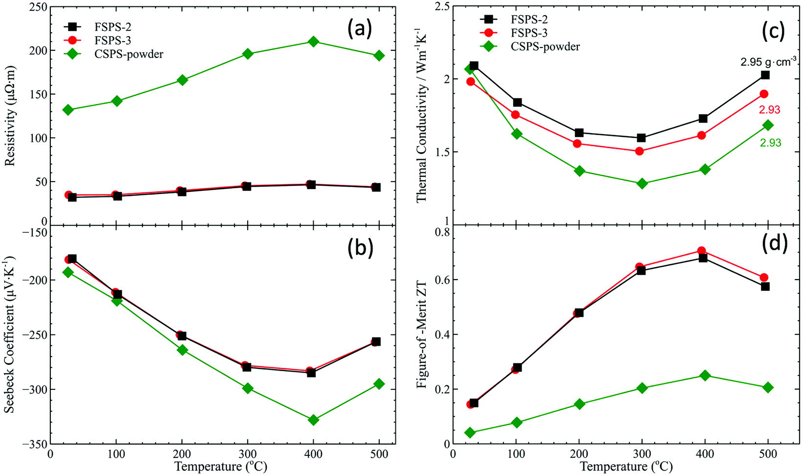 | ||
| Fig. 7 Temperature dependence of (a) resistivity, (b) Seebeck coefficient, (c) thermal conductivity, and (d) figure-of-merit ZT for FSPS-2, FSPS-3 and CSPS-powder samples. | ||
Conclusions
Flash sintering using direct current with a heating rate of 1000 °C min−1 was performed on MSS green compacts in a SPS furnace without the use of a die or conductive wrapping. The sufficient electrical conductivity of the green compacts facilitated the direct heating of samples from room temperature, and opened up a sintering window of 6 s in a ∼40 s sintering process. To clarify the influence of local Joule heating at the grain contacts on phase evolution and surface oxide re-distribution, the temperature and oxygen-sensitive solid solution Mg2.1Si0.487Sn0.5Sb0.013 was carefully chosen as an example material to demonstrate the capability of flash sintering of TE materials. Compared with the weak or mild phase separation in conventional SPS samples, the flash sintered samples exhibited significant phase segregation because of local melting at the grain contacts created by local Joule heating. Part of the surface oxide in the flash sintered samples was wrapped in the tin-rich phase as a result of the melting and movement of connecting necks between adjoining particles; this is instead of being translated into the grain boundaries as occurred in the CSPS samples prepared directly from powder. Both the re-distribution of surface oxide and precipitation of a tin-rich phase lowered the resistivity of the FSPS samples by creating a charge carrier highway network. The resistivity of the FSPS samples was four times lower than that of the CSPS-powder sample prepared from the same powder. These preliminary results suggest that the flash sintering with direct Joule heating could be a potential die-less rapid densification route for TE materials, which can maintain the nanostructure of powders and optimise the distribution or removal of grain/agglomerate surface oxidation.Acknowledgements
This work was supported by a Marie Curie International Incoming Fellowship of the European Community Human Potential Program under Contract no. PIIF-GA-2013-622847. We would also like to acknowledge the support of European Thermodynamics Ltd (ETL). MJR and AM would also like to acknowledge the support of The Engineering and Physical Sciences Research Council (EP/L017695/1, MASSIVE). BD also thanks the financial supports of the National Science Foundation of China (Grant No. 51202060).References
- Handbook of Thermoelectrics: Macro to Nano, ed. D. M. Rowe, CRC Press/Taylor & Francis, Boca Raton, FL, 2006 Search PubMed.
- J. Yang, 24th International Conference on Thermoelectrics, 2005, pp. 170–174 Search PubMed.
- L. E. Bell, Science, 2008, 321, 1457–1461 CrossRef CAS PubMed.
- G. A. Slack, New materials and performance limits for the thermoelectric cooling, CRC Handbook of Thermoelectrics, CRC Press, Boca Raton, FL, 1995 Search PubMed.
- K. Zweibel, Science, 2010, 328, 699–701 CrossRef CAS PubMed.
- S. Hudgens and B. Johnson, MRS Bull., 2004, 29, 829–832 CrossRef CAS.
- A. Saramat, G. Svensson, A. E. C. Palmqvist, C. Stiewe, E. Mueller, D. Platzek, S. G. K. Williams, D. M. Rowe, J. D. Bryan and G. D. Stucky, J. Appl. Phys., 2006, 99, 023708 CrossRef.
- A. Saramat, G. Svensson, A. E. C. Palmqvist, C. Stiewe, E. Mueller, D. Platzek, S. G. K. Williams, D. M. Rowe, J. D. Bryan and G. D. Stucky, Handb. Cryst. Growth, 2015, 281–329 Search PubMed.
- B. Du, Y. Saiga, K. Kajisa and T. Takabatake, Chem. Mater., 2015, 27, 1830–1836 CrossRef CAS.
- Y. X. Chen, K. Niitani, J. Izumi, K. Suekuni and T. Takabatake, J. Cryst. Growth, 2014, 402, 312–318 CrossRef CAS.
- H. H. Hausner, Modern Developments in Powder Metallurgy: Volume 1: Fundamentals and Methods, Springer Science & Business Media, 2012 Search PubMed.
- C.-N. Liao, L.-C. Wu and J.-S. Lee, J. Alloys Compd., 2010, 490, 468–471 CrossRef CAS.
- J. R. Drabble and C. H. L. Goodman, J. Phys. Chem. Solids, 1958, 5, 142–144 CrossRef CAS.
- B. Poudel, Q. Hao, Y. Ma, Y. Lan, A. Minnich, B. Yu, X. Yan, D. Wang, A. Muto, D. Vashaee, X. Chen, J. Liu, M. S. Dresselhaus, G. Chen and Z. Ren, Science, 2008, 320, 634–638 CrossRef CAS PubMed.
- K. Komoto and T. Mori, Thermoelectric Nanomaterials: Materials Design and Applications, Springer, 2013 Search PubMed.
- O. Guillon, J. Gonzalez-Julian, B. Dargatz, T. Kessel, G. Schierning, J. Räthel and M. Herrmann, Adv. Eng. Mater., 2014, 16, 830–849 CrossRef CAS.
- S. Grasso, Y. Sakka and G. Maizza, Sci. Technol. Adv. Mater., 2009, 10, 53001 CrossRef PubMed.
- M. Ito and K. Kawahara, Mater. Trans., 2015, 56, 2023–2028 CrossRef CAS.
- S. Bathula, M. Jayasimhadri, B. Gahtori, N. K. Singh, K. Tyagi, A. K. Srivastava and A. Dhar, Nanoscale, 2015, 7, 12474–12483 RSC.
- N. Chawake, L. D. Pinto, A. K. Srivastav, K. Akkiraju, B. S. Murty and R. S. Kottada, Scr. Mater., 2014, 93, 52–55 CrossRef CAS.
- J. Gonzalez–Julian, K. Jähnert, K. Speer, L. Liu, J. Räthel, M. Knapp, H. Ehrenberg, M. Bram and O. Guillon, J. Am. Ceram. Soc., 2016, 99, 35–42 CrossRef.
- M. Cologna, B. Rashkova and R. Raj, J. Am. Ceram. Soc., 2010, 93, 3556–3559 CrossRef CAS.
- M. Cologna and R. Raj, J. Am. Ceram. Soc., 2011, 94, 391–395 CrossRef CAS.
- S. Grasso, T. Saunders, H. Porwal, O. Cedillos-Barraza, D. D. Jayaseelan, W. E. Lee and M. J. Reece, J. Am. Ceram. Soc., 2014, 97, 2405–2408 CrossRef CAS.
- S. Grasso, T. Saunders, H. Porwal, B. Milsom, A. Tudball and M. Reece, J. Am. Ceram. Soc., 2016, 99, 1534–1543 CrossRef CAS.
- B. Niu, F. Zhang, J. Zhang, W. Ji, W. Wang and Z. Fu, Scr. Mater., 2016, 116, 127–130 CrossRef CAS.
- E. Castle, R. Sheridan, S. Grasso, A. Walton and M. Reece, J. Magn. Magn. Mater., 2016, 417, 279–283 CrossRef CAS.
- O. Vasylkiv, H. Borodianska, Y. Sakka and D. Demirskyi, Scr. Mater., 2016, 121, 32–36 CrossRef CAS.
- W. Liu, X. Tan, K. Yin, H. Liu, X. Tang, J. Shi, Q. Zhang and C. Uher, Phys. Rev. Lett., 2012, 108, 166601 CrossRef PubMed.
- W. Liu, Q. Jie, H. S. Kim and Z. Ren, Acta Mater., 2015, 87, 357–376 CrossRef CAS.
- H. Ning, G. D. Mastrorillo, S. Grasso, B. Du, T. Mori, C. Hu, Y. Xu, K. Simpson, G. Maizza and M. J. Reece, J. Mater. Chem. A, 2015, 3, 17426–17432 CAS.
- K. Yin, X. Su, Y. Yan, C. Uher and X. Tang, RSC Adv., 2016, 6, 16824–16831 RSC.
- I.-H. Jung, D.-H. Kang, W.-J. Park, N. J. Kim and S. Ahn, CALPHAD: Comput. Coupling Phase Diagrams Thermochem., 2007, 31, 192–200 CrossRef CAS.
- R. Viennois, C. Colinet, P. Jund and J.-C. Tédenac, Intermetallics, 2012, 31, 145–151 CrossRef CAS.
- W. Liu, X. Tang, H. Li, K. Yin, J. Sharp, X. Zhou and C. Uher, J. Mater. Chem., 2012, 22, 13653–13661 RSC.
- C. Schmerbauch, J. Gonzalez-Julian, R. Röder, C. Ronning and O. Guillon, J. Am. Ceram. Soc., 2014, 97, 1728–1735 CrossRef CAS.
- J. J. Martin, J. Phys. Chem. Solids, 1972, 33, 1139–1148 CrossRef CAS.
| This journal is © The Royal Society of Chemistry 2017 |