
 Open Access Article
 This Open Access Article is licensed under a
 Creative Commons Attribution 3.0 Unported Licence
Process–property relationship in high-k ALD SrTiO3 and BaTiO3: a review
J. H.
Shim†
*ab,
H. J.
Choi†
 a,
Y.
Kim†
b,
J.
Torgersen
bc,
J.
An
*d,
M. H.
Lee
*e and
F. B.
Prinz
*bf
a,
Y.
Kim†
b,
J.
Torgersen
bc,
J.
An
*d,
M. H.
Lee
*e and
F. B.
Prinz
*bf
aSchool of Mechanical Engineering, Korea University, 145 Anam-ro, Seongbuk-gu, Seoul 02841, Korea. E-mail: shimm@korea.ac.kr
bDepartment of Mechanical Engineering, Stanford University, Stanford, CA 94305, USA. E-mail: fbp@cdr.stanford.edu
cDepartment of Engineering Design and Materials, Norwegian University of Science and Technology, Trondheim 7491, Norway
dManufacturing Systems and Design Engineering (MSDE) Program, Seoul National University of Science and Technology, 232 Gongneung-ro, Nowon-gu, Seoul 01811, Korea. E-mail: jihwanan@seoultech.ac.kr
eSchool of Engineering, University of California Merced, Merced, CA 95343, USA
fDepartment of Materials Science and Engineering, Stanford University, Stanford, CA 94305, USA
First published on 8th June 2017
Abstract
Perovskites exhibit a wide range of remarkable material properties that have the potential to advance various scientific fields. These properties originate in their unique structure and composition. To leverage these properties in the ultrathin film regime, atomic-level control of thickness, composition, and crystal structure will be essential for creating next-generation perovskite devices. Atomic layer deposition (ALD) has the potential to enable these design prospects. However, its future use in the field will be dependent on the quality of the link between ALD process parameters and the perovskite phase. In this overview, we present work on barium and strontium titanate (BTO and STO) ultrathin films for high-k applications. We present ALD process strategies developed and optimized to achieve both desired composition and phase, yielding high dielectric constants and low leakage currents at the same time. We discuss thermal annealing, plasma treatment, and the use of seed layers and specialized precursors to improve the properties of BTO and STO by different enhancement mechanisms. In the ultrathin film regime, the understanding of macroscopic material properties will be dependent on the knowledge of the atomic scale arrangement. In conjunction with advances in manufacturing, we therefore also discuss novel strategies and techniques for characterization that will likely be significant in establishing a valid and reliable ALD process parameter–thin film dielectric property relationship.
1. Introduction
1.1 Atomic layer deposition
Atomic layer deposition (ALD) is a thin film fabrication technique that uses a vaporized source for a chemical surface reaction. In this respect, the ALD process is regarded as a derivative of chemical vapor deposition (CVD). Unlike in CVD, however, in ALD, film deposition occurs via the self-saturating mechanism. In the first cycle of ALD, with the first precursor source containing the target component, “A,” the self-saturating reaction forms layers of the “A” material but stops growing at some specific thickness, usually one atomic layer or less, independent of the supply of vaporized precursors. The film growth can be continued by changing the precursor source to a different material, “B,” but again, the film growth stops at a critical atomic thickness regardless of the precursor dose. By alternating the “A” and “B” cycles at an appropriate ratio, ALD can produce A–B compound films with a desired composition. This process is illustrated in Fig. 1(a). Owing to its self-saturating characteristic, ALD can achieve a uniform thickness over large areas of substrate surfaces (e.g. thickness error of less than 1% for an area of 240 mm diameter),1 while in CVD, the film growth rate is heavily dependent on the dose and supply direction of the source chemicals. (Fig. 1(b) shows the comparison of a variety of thin-film deposition techniques).2 Depending on the choice of substrate and film materials, the films initially form either solid layers or islands, depending on the relation between their respective energies. With these advantages and design opportunities, ALD has been utilized for successfully fabricating ultrathin films, nano-laminating layers, and conformal surface coatings in high-aspect-ratio trenches, on rods, tubes, and particles.3–9 Examples of uniform ALD coatings on the nano-scale are well summarized in a paper published by Pinna et al.10 Another advantage of ALD is its relatively low process temperature, generally under 400 °C. In a special case of ALD with Al2O3 using trimethyl alumina (TMA) and water as precursors, the ALD process can be conducted even at room temperature. This minimizes the thermal stresses between the layers, reducing related problems such as film breakage or delamination. In addition, due to the low process temperatures, a wide range of substrates can be coated, from ceramic wafers to polymers and organic fabrics.11–14 However, the low deposition temperature can also inhibit a high degree of crystallization, which is closely related to the electrical properties of the ALD film leading to a low dielectric constant.15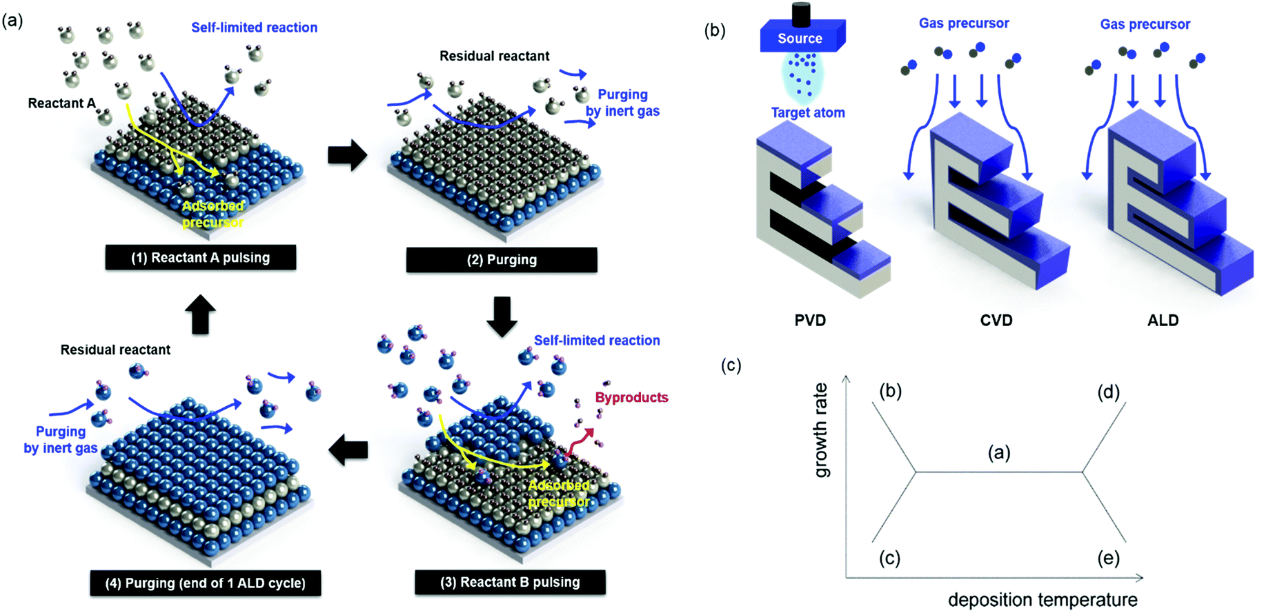 | ||
| Fig. 1 (a) ALD process for A–B compound films, (b) a comparison of other film deposition techniques, and (c) the ALD growth mode as determined by process temperatures: a. optimal ALD window, b. precursor condensation regime, c. insufficient reaction regime, d. precursor decomposition regime, and e. precursor desorption regime due to source characteristics. | ||
ALD has been developed to meet the demand for the fabrication of ultrathin electroluminescent films and dielectric layers for semiconductor devices.16–29 As an arbitrarily scalable vacuum technique, ALD can be easily integrated in modern chip manufacturing. It finds broad applicability for depositing high-k dielectric layers in metal–insulator–metal capacitors for dynamic random access memory (DRAM) and for fabricating gate oxides in complementary metal–oxide–semiconductor (CMOS) transistors. The state-of-the-art DRAM capacitors currently require structures with high-aspect-ratios (80–100), which have become indispensable for semiconductor devices with dimensions below 100 nm, and the ALD process is currently being used for this type of device production.29
1.2 Need of ultra-thin high-k films for DRAM capacitors
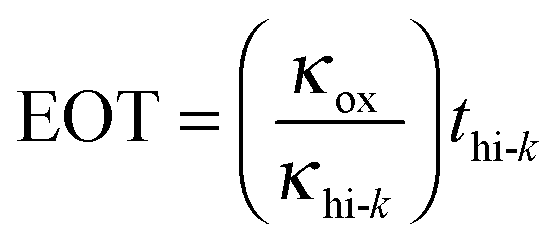
The dielectric material is an insulator that exhibits dielectric polarization under an electric field. Owing to dielectric polarization, the positive charge of the dielectric material shifts in the direction of the electric field while the negative charge moves in the opposite direction of the electric field. The degree of shift determines the dielectric constant, which is an important electrical property for the performance of a semiconductor device. Dielectric materials have received much attention owing to their applications in microelectronics. The most straightforward applications of dielectric films are in conventional DRAM capacitors. DRAM has capacitor-based memory, while the two states of a capacitor (i.e., charged or discharged) represent the two values of a bit. Capacitance (C) is an important electrical property that is expressed by the well-known equation below: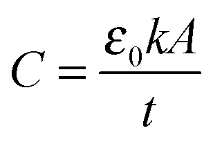 | (1.2.1) |
 | (1.2.2) |
As seen in eqn (1.2.1), there are three parameters that can be adjusted to address the aggressive scale-down trend: (1) increasing A by making the capacitor feature more corrugated, as shown in Fig. 2, (2) increasing the dielectric constant of the capacitor oxide, and (3) decreasing the oxide thickness. As achieving a higher A involves highly complicated geometry that can increase the fabrication cost, a breakthrough in enhancing the capacitance is achievable by only realizing a very low EOT (i.e., a very high k/t). The international roadmap for semiconductors defines the EOT target as <0.3 nm, making the use of high-k materials inevitable.30
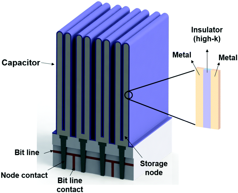 | ||
| Fig. 2 Simplified schematic diagrams of a DRAM capacitor. | ||
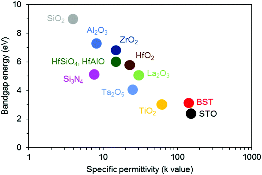 | ||
| Fig. 3 Bandgap energy and specific permittivity of various materials. Reproduced from ref. 52. © 2010 Sunami H. Published in “Advances in solid state circuit technologies” under CC BY-NC-SA 3.0 license. Available from: http://dx.doi.org/10.5772/8638. | ||
1.3 SrTiO3 and BaTiO3 as high-k dielectric perovskites
Perovskite oxides are materials with the chemical formula ABO3 wherein A and B generally represent cations with charges of 2+ and 4+, respectively, or 3+ and 3+, respectively. The B4+/3+ ions are neighbored by six oxide ions, whereas the A2+/3+ ions are coordinated with twelve oxide ions at the nearest neighbor distances. The ideal perovskite oxide cubic structure belongs to the space group Pm3m in the reference state, while deviations in temperature and pressure from the reference conditions can easily transform the crystal structure from cubic to tetragonal, octahedral, orthorhombic, or rhombohedral. For example, BaTiO3 (BTO) has a cubic symmetry at atmospheric pressure above the temperature of 120 °C, which is called the Curie transition temperature, under which the material transforms into the tetragonal, orthorhombic (<10 °C), or rhombohedral (<−90 °C) structure.31–33 The ionic radius of A ions is relatively large compared to that of B ions. SrTiO3 (STO), the most representative dielectric perovskite oxide, has ionic radii of Sr2+ = 1.44 Å and Ti4+ = 0.605 Å in the ideal cubic crystals under standard atmospheric conditions.34 The symmetry of perovskite materials is easily distorted due to this relatively large difference in the cation sizes. Most perovskite oxides are insulators in the cubic phase, while variations in the crystallinity induce metallic, superconducting, ferroelectric, and ferromagnetic properties.35–42 BTO exhibits simple dielectric properties with cubic symmetry. Transitioning to the tetragonal structure, spontaneous dipole moments arise with the bistable positioning of Ti4+ ions in the O6 octahedra; this results in the well-known ferroelectricity of BTO while STO has paraelectricity at room temperature.43 The dielectric constant of perovskites such as BTO and STO is usually higher than that of binary oxides. This dielectric property can be explained by polarizability, which is the degree of charge separation under an electric field. A large polarizability can lead to large dipole moments, which can lead to high dielectric constants. In the case of perovskites such as BTO and STO, the polarizability is much greater than the binary oxides because of the high travel distance of Ti4+ in the O6 octahedral structure under an electric field.44 Thus, BTO and STO can exhibit much higher dielectric constants than SiO2 and Al2O3. For a more detailed comparison, the dielectric constants of the main dielectric materials are given in Fig. 3 and Table 1.45–522. Perovskite phase in the ultrathin-film regime
Exploring the fundamental limits in thickness seems especially difficult with perovskites. In the nanometer regime, i.e., at length scales relevant to the microelectronics industry, perovskites approach length scales associated with their structure-determined material characteristics.53 Due to several scaling effects, some key properties are strongly thickness dependent.54 Deviations from the infinitely large and ideal crystalline state occur during material synthesis and affect regions in the thin film responsible for the material's paraelectric and ferroelectric properties.55One can distinguish between intrinsic and extrinsic effects. Intrinsically, defects cause crystal sizes and domain walls to decrease until crystal-like perovskite particles become a single domain. The phase transitions of the material propagate, thereby decreasing the dielectric response.56
Extrinsic effects are related to the boundary conditions of the material. Properties related to perovskites necessitate a surface termination of the electrical polarization, in which the normal component of the displacement is continuous. At the interfaces, this situation cannot exist unless there is sufficient compensating charge.56,57
These effects cause the material to lose its ferroelectric properties when approaching the nanometer regime.53 The difficulty of thin-film processing has posed challenges for the industrial implementation of ultrathin perovskites in the microelectronics industry. However, knowledge obtained from longstanding extensive research has equipped researchers with certain design rules and knowledge on ideal thin-film perovskite structures for high-k applications:54
• The dielectric properties of the material should not change in the temperature range of operation, which means that the material should always stay in one phase.58 The phase can be stabilized, for example by using dopants.59
• The crystal structure shall be uniform to prevent grain boundaries and crystal dislocations favoring carrier recombination and potential leakage paths.
• Due to a linear capacitive charge and a relatively slow polarization reversal process in the saturation arm of the hysteresis loop, ferroelectric films are undesirable for DRAM applications.60 They cause an increase in loss tangent and a limit in the charging and discharging speed of capacitors. Instead, cubic paraelectric films show no remnant polarization when the field is removed and the lattice should easily relax back to the previous state.61
• The dielectric properties of both BTOs and STOs are strongly thickness dependent.53,62 This is due to grain size and stress induced by the substrate. Larger grains increase the electron mobility63 and lattice mismatches between the substrate and the film induce different structural distortions changing the perovskite properties.
To overcome induced structural distortions, capacitor electrodes should meet the thermal expansion coefficient and lattice of the perovskite film to avoid strain during synthesis and operation. Furthermore, diffusion of the electrodes into the semiconductor film has to be avoided to prevent the formation of a depletion layer with parasitic capacitance.
These design rules are general and independent of the fabrication technique. However, ALD approaches a thickness regime where not only processing poses significant challenges. The desired perovskite thin films are often morphologically complex, ultrathin, and therefore challenging to characterize. For example, mostly amorphous BTO with embedded crystalline moieties that provides a good tradeoff between low leakage current and high dielectric constant cannot be characterized with conventional X-ray diffraction (XRD).64,65 In the following sections, we will review the strategies that have been developed to date for achieving high-performance perovskite thin films using ALD, particularly for STO and BTO. In addition, we will outline the characterization techniques that provide insights into the structure, composition, and dielectric properties of ALD perovskites.
3. Recent approaches to produce high-quality ALD STO and BTO
3.1 Challenges related to ALD perovskite thin film deposition
The ALD method has advantages such as self-limited reaction that makes it possible to deposit thin films of uniform thickness on complex shaped substrates. Thus, the technique can be used in the production of high-k perovskites for DRAM capacitors. However, there are some problems in manufacturing high-k perovskites using ALD. First, the low processing temperatures (generally below 350 °C) of ALD perovskites are generally not sufficient to crystallize the film. The low deposition temperature of ALD perovskites is caused by the narrow process windows of the ALD precursors. Perovskites with low crystallinity can have a lower dielectric constant than a crystallized film due to the loss of the crystal structure in the B-site octahedron, which can significantly contribute to the polarizability of perovskites.15,44 Therefore, it is necessary to develop an appropriate crystallization treatment to achieve high dielectric constant characteristics. Second, ALD perovskites can be easily contaminated by carbonates and hydroxides, which can increase the leakage current of the film. Contamination during the ALD process is possible owing to incomplete removal of the precursor ligand; it can also be due to the inherent vulnerability of the material to contamination by carbon and hydroxyl species.66 Furthermore, it is very important to minimize impurities and defects in dielectric thin films because of their severe negative effect, as they can possibly lead to high leakage current. Third, it is still unclear how the properties of ALD ultrathin perovskites are different from the bulk perfect crystal. While the characterization of the bulk crystal is relatively robust, the nanostructure, chemical concentration, and crystallinity of ALD ultrathin perovskites are complicated and difficult to understand. Furthermore, the focus of most recent research is on tuning the film's composition, morphology and crystal structure in various ways to improve its electrical properties. Therefore, it is important to understand the properties of ALD ultrathin films by using a powerful characterization tool as the key factor that links the ALD process to the film's electrical properties. In the subsequent sections, we will present a study on the development of STO and BTO ALD processes, and the development of high-performance ultrathin perovskite DRAM capacitors using the latest approaches such as thermal annealing, plasma treatment, and the use of seed layers and special precursors, and ALD perovskite thin film characterization techniques.3.2 Thermal annealing (annealing during every ALD cycle or post-deposition annealing)
Thermal annealing is important to improve the quality of ALD perovskite films; the thermal excitation causes the constituent atoms to move to an energy-stable position. This increases the crystallinity of the perovskite structure and contributes to the removal of defects or impurities which are responsible for the electron leakage path. Depending on the timing, thermal annealing can be divided into in-cycle annealing (ICA) and post-deposition annealing (PDA). The former method anneals samples between deposition cycles, while the latter method anneals samples after all deposition cycles are over. ICA is not desirable for two reasons. First, to maintain a high process throughput, heating and cooling between the ALD process temperature and the annealing temperature must take place in a very short period of time to avoid an appreciable increase of the ALD cycle time.67,68 Second, crystallization, which is strongly dependent upon the film thickness, is less likely to occur at the early stage of deposition, and a very thin film (<10 nm) requires much higher temperatures for crystallization.69 However, as a more advanced ICA method enabling shorter annealing times without alternating between substrate temperatures, flash-lamp annealing (FLA) might be a plausible option for ICA, wherein specimens are exposed to high-intensity visible light pulses on the order of milliseconds, and the temperature of the light-exposed surface reaches the annealing temperature.67 It is desirable to anneal ALD films during every ALD cycle utilizing a short time scale and low thermal budget heating method. However, FLA has a significant drawback for 3-D structures due to the directionality of light and the consequent shading effect.PDA has been extensively studied for STO70–75 and BTO.66,69,76 Vehkamäki et al. reported the post-annealing of STO and BTO films with different Sr/(Sr + Ti) or Ba/(Ba + Ti) atomic ratios in air at 500 °C for 1 h. They achieved the highest dielectric constants reported thus far, i.e., 180 and 165 from stoichiometric STO and BTO, respectively.70 Another report from the same group,66 using a different barium precursor, Ba(tBu3Cp)2 (tBu3Cp = tris(tert-butyl-cyclopentadienyl)), which is more chemically stable up to 340 °C and shows a higher deposition rate, showed the effect of PDA on the electrical performance of 32 nm stoichiometric BTO at 600 °C under O2 to increase the permittivity of the film from 15 (as-deposited) to 70 (annealed) by forming the cubic phase of BTO while maintaining a low leakage current density (JG) of <10−7 A cm−2 at 1 V.66 With the same precursors and the PDA protocol, BTO films with various Ba stoichiometries (Ba/(Ba + Ti) = 33–52 at%) and thicknesses (32–140 nm) were prepared, and the degree of crystallization after post-deposition annealing was studied; more stoichiometric BTO tended to be more easily crystallized.76 Pawlak et al. at IMEC, Belgium, extensively studied the PDA effects on the crystallization behavior of stoichiometric or Sr-rich SrxTiyOz ALD films.72 After thermal annealing at 500–600 °C under N2, stoichiometric STO films (9–10 nm) showed a dielectric constant of >200, although they suffered from a high leakage current (10−2 to 10−3 A cm−2 at 1 V), due to the formation of nanocracks induced by large crystalline grains. Sr-rich STO (Sr/(Sr + Ti) = ∼64 at%, 9–10 nm), however, showed a dielectric constant of ∼50 with a low JG of 10−6 A cm−2 at 1 V, which is a largely improved leakage current with some sacrifice of the dielectric constant due to its different crystallization behavior. It also exhibited a smaller grain size, no detectable cracks and bulk-limited trap-assisted leakage, independent of the electrode.
The effect of the A-site cation ratio of SrxTiyOz (thickness = 3–20 nm, Sr/(Sr + Ti) = 45–67 at%) on the crystallization behavior upon post-annealing has been more extensively studied by in situ XRD phase analyses.73 The Sr/(Sr + Ti) atomic ratio strongly influences the crystallization temperature and texture/morphology of crystallized samples. Stoichiometric STO showed a crystallization temperature range (530–550 °C) lower than other STO compositions, and for stoichiometric STO, thinner STO (thickness, 5 nm; crystallization temperature, 550 °C) requires a higher crystalline temperature than that of thicker STO (thickness, 10 nm; crystallization temperature, 530 °C). Table 2 summarizes the annealing conditions of various ALD high-k films from previously reported articles.
| Reactant A/reactant B | A-site cation ratio (at%, Sr/(Sr + Ti) or Ba/(Ba + Ti)) | Thickness (nm) | T annealing (°C) | Annealing environment | Ref. | |
|---|---|---|---|---|---|---|
| Vehkamäki et al. | ||||||
| SrxTiyOz | Sr(iPr3Cp)2/Ti(OiPr)4 | 40–60 | 500 | Air | 70 | |
| BaxTiyOz | Ba(CpMe5)2/Ti(OiPr)4 | 50 | 500 | Air | 70 | |
| BaxTiyOz | Ba(tBu3Cp)2/Ti(OMe)4 | 51–52 | 32 | 600 | O2 | 66 |
| BaxTiyOz | Ba(tBu3Cp)2/Ti(OMe)4 | 33–52 | 32–140 | 600 | O2 | 76 |
| Kessel et al. | ||||||
| SrxTiyOz | Sr(iPr3Cp)2DME/CpMe5Ti(OMe)3 | 46–57 | 15–30 | 600/650 | N2 | 71 |
| SrxTiyOz | Sr(iPr3Cp)2DME/CpMe5Ti(OMe)3 | 42–68 | 30–40 | 600 | N2 | 78 |
| IMEC | ||||||
| SrxTiyOz | Sr(tBu3Cp)2/Ti(OMe)4 | 50, 66 | 9–10 | 500–600 | N2 | 72 |
| SrxTiyOz | Sr(tBu3Cp)2/Ti(OMe)4 | 45–67 | 3–20 | 525–700 | N2 | 73 |
| Hwang et al. | ||||||
| SrxTiyOz | Sr(iPr3Cp)2/Ti(O-iPr)2(tmhd)2 | 39–68 | 18–22 | 650 | N2 | 79 |
| SrxTiyOz | Sr(iPr3Cp)2/Ti(O-iPr)2(tmhd)2 Ti(Me5Cp)(OMe)3 | 650 | N2 | 80 | ||
3.3 Use of plasma (intra-deposition & post-deposition)
While processing techniques such as thermal annealing or seed layering can provide high-quality ALD perovskite films, these techniques often necessitate a high processing temperature (>600 °C), which may damage the underlying components. In contrast, engineering the properties of ALD perovskite films by plasma treatment could be advantageous so that further elevating the processing temperature is not needed. For example, the level of crystallization, which largely affects the electrical properties of films, can be easily tuned by facilitating the ionic bombardment inside the plasma on the top surface of the films; the kinetic energy transferred from the bombardment into the film induces the formation of crystalline nucleates. Two different kinds of plasma depending on the location where the plasma is generated could be utilized for the treatment of thin films: direct plasma and remote plasma. Direct plasma is known to generate a high density and flux of ions close to the substrates. Therefore, it is advantageous in crystallizing thin films but could cause structural damage. In contrast, remote plasma is known to generate a relatively lower density and flux of ions (a few orders of magnitude lower), which in many cases is energetically insufficient for crystallizing thin films. A recent paper from Stanford University reported the possibility of utilizing remote plasma in crystallizing ALD TiO2 thin films.77 Meanwhile, both types of plasma, i.e., direct and remote oxygen plasma, are also advantageous to the oxidation of ALD films due to the high chemical reactivity of radicals and ions in the plasma. Such enhanced oxidation widens up the process flexibility: the deposition of perovskite thin films using less reactive metal precursors has been reported to be feasible when oxygen plasma is used.Plasma treatment can be incorporated into the ALD process for perovskite films in two different ways: intra-deposition and post-deposition treatments. Intra-deposition plasma treatment is conducted between ALD cycles; therefore, we could regard the plasma step in plasma-enhanced ALD (PEALD) cycles, where plasma treatment (usually oxygen plasma) replaces the oxidation step by water or oxygen in thermal ALD, as a type of intra-deposition plasma treatment. Intensive research has been conducted in the area of plasma utilization for intra-deposition treatment of ALD perovskite films, mostly STO films (Table 3).64,78,81–93 Kil et al. showed that the oxygen remote plasma (9 s) could be used for depositing STO films using Sr(METHD)2 (METHD = methoxyethoxy–tetramethyl–heptanedionate) even at a relatively low temperature (∼250 °C) without detectable impurities (detection limit ∼0.1 at%).81–84 Notably, the diketonate Sr precursor, which had been reported not to react with the most common oxygen sources, successfully reacted with remote oxygen plasma. Remote-plasma-activated H2O was also used to oxidize the diketonate Sr precursor, resulting in the deposition of a STO film with a high dielectric constant (∼95).84 Such a high dielectric constant may imply the partial crystallization of the film by virtue of the energetic plasma species. The use of oxygen plasma for partially crystallized STO was also reported, and the dielectric constant of the resulting STO was 65 at 50 nm.85 Plasma-activated H2O was not effective in crystallizing STO films, resulting in a very low dielectric constant (∼20).86 ALD STO treated by oxygen plasma (150 W) showed partial crystallinity in the XRD spectra at thicknesses >20 nm on the Ru bottom electrode.87 STO films based on a Cp-based Sr precursor and remote oxygen plasma were also amorphous.78,90–92 A recent report by Prinz et al. showed that the crystallinity of thermally grown ALD BTO could be improved by a remote oxygen plasma treatment after deposition (i.e., post-deposition treatment);64 the dielectric constant of the ALD BTO increased by about a factor of 2 after extensive exposure (3 hours) to remote oxygen plasma due to the partial crystallization of the BTO film surface. Prinz et al. also reported the PEALD of BTO films with remote oxygen plasma.93 In this report, they showed the formation of 1–2 nm crystallites embedded in the amorphous matrix, whereas thermal ALD BTO appeared to be completely amorphous.
| Main material | Plasma type | Intra-or post-deposition | Deposition temperature (°C) | Crystallinity | Thickness (nm) | EOT (nm) | Leakage current density (A cm−2) | Ref. |
|---|---|---|---|---|---|---|---|---|
| STO | Remote O2 plasma | Intra | 280 | — | 17.6 | 1.2 | 2 × 10⁻⁶ @ 1 V after post-annealing | 82 |
| 225 | Amorphous without the SrO seed layer/slightly crystalline on the SrO seed layer | 10 | 0.5 | — | 87 and 88 | |||
| 250 | Amorphous | 34.7 | 2.4 | 1 × 10⁻⁷ @ 1 V | 90 | |||
| 250 | Amorphous | 16.7 | 1.5 | — | 91 | |||
| Remote-plasma-activated H2O vapor | Intra | 250 | Mixed phases (crystalline + amorphous) | 19.5 | 0.8 | 1.98 × 10⁻⁶ @ 1 V after post-annealing | 83 and 84 | |
| 190–270 | Amorphous | 20 | 0.45 | 1 × 10⁻³ @ 1 V after post-annealing | 86 | |||
| BTO | Remote O2 plasma | Post | 250 | Slightly crystalline after 3 h of plasma treatment | 5 | 0.38 | 3 × 10⁻⁴ @ 1.6 V | 64 |
| Intra | 250 | Slightly crystalline | 12 | 3.2 | ∼10−7 @ 1.6 V | 93 | ||
3.4 Seed layer scheme
Seed layering is a well-known scheme for crystallizing ALD films (Table 4). For seed layering, an extremely thin seed layer (usually <5 nm thick) is deposited on the substrate and annealed at a high temperature (600–700 °C), usually with rapid thermal annealing (RTA) for several minutes. The seed layer thin film is then fully crystallized and helps the overlying main film to be crystallized more easily, which is crucial for achieving high capacitance.| Main material | Seed layer material | Main material thickness (nm) | Seed layer thickness (nm) | Deposition temperature/seed layer annealing temperature (°C) | EOT (nm) | Leakage current density (A cm−2) | Ref. |
|---|---|---|---|---|---|---|---|
| STO | STO | 20 | 5 | 250/650 | 0.45 | 1 × 10⁻³ @ 1 V | 86 |
| 20 | 3 | 370/700 | 0.72 | 1 × 10⁻⁷ @ 0.8 V | 15 | ||
| 10 | 1.35 (optimal) | 225/600 | 0.5 | — | 87 | ||
| 20 | 3–5 | 370/650–700 | 0.6 | 1 × 10⁻⁸ @ 0.8 V | 94 | ||
| 10 | 2.7 | 225/600 | 0.5 | — | 88 | ||
| 15–20 | 5 | 250/700 | 0.76 | 1.7 × 10⁻⁷ @ 0.8 V | 95 | ||
| 10 | 4–6 | 370/700 | 0.65 | 1 × 10⁻⁶ @ 1 V | 96 | ||
| SrO | 10 | 1.35 (optimal) | 225/600 | 0.5 | — | 87 | |
| 10 | 2.7 | 225/600 | 0.5 | — | 88 |
Hwang and coworkers used a 5 nm thick STO seed layer annealed at 650 °C for 1 min with RTA, which resulted in an improvement in the capacitance (2.7 μF cm−2 without a seed layer vs. 4.5 μF cm−2 with a seed layer) and a decrease in the JG (10−1 A cm−2 without a seed layer vs. 10−5 A cm−2 with a seed layer at 1 V) of the main STO layer.86 They also reported a 3 nm thick STO seed layer annealed at 600–750 °C for 1 min with RTA. The capacitance of a 17 nm thick main STO layer significantly increased by a factor of 5.15 A thin SrO layer has also been used as the seed layer for STO deposition: Roh et al. reported that the SrO seed layer (with the optimal thickness of 1.35 nm) on a Ru substrate annealed at 600 °C for 10 min with RTA becomes SrRuO3, which is also a perovskite (Fig. 4). The main STO films on the SrO seed layer showed a dielectric constant as high as ∼80 and a strong STO peak in XRD even at 10–15 nm thicknesses.87
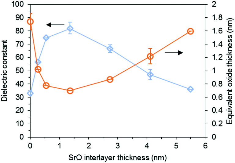 | ||
| Fig. 4 Dependence of the dielectric properties of 15 nm thick STO film on the thickness of the inserted SrO layer.87 Reprinted with permission from J. Electrochem. Soc., 155, 2008, G185. Copyright 2008, The Electrochemical Society. | ||
Hwang et al. further investigated the annealing temperature for seed layer crystallization: they discovered that the 3–5 nm STO seed layer annealed at <600 °C weakly crystallizes, resulting in poor crystallization of the main-layer STO. On the other hand, an annealing temperature of 750 °C induced adverse chemical interactions between the seed STO and the Ru electrode. Therefore, seed layer annealing temperatures of 650 to 700 °C were optimal in achieving the highest k (∼110) in STO films.94 Meanwhile, Ahn et al. reported that a 2.7 nm SrO seed layer on RuO2 annealed at 600 °C is optimal for obtaining the maximum k for main STO film (∼160) compared to that of k = 85 and 91 for films deposited directly on Ru and via seeds formed on the Ru substrate, respectively.88 Menou et al. used a 5 nm STO seed layer annealed at 700 °C for 2 min with a Levitor tool. They reported that using a seed layer lowers the annealing temperature of the main STO layer for crystallization, which is beneficial for preventing oxidation in TiN bottom electrodes.95 Popovici et al. reported that a 4–6 nm STO seed layer annealed at 700 °C for 1.5 s using a spike anneal in He on TiN offers the advantages of eliminating nanocracks and consequently lower leakage, but with a slightly increased EOT (probably due to the presence of an amorphous thin layer on the top surface).96
3.5 Use of specialized precursors
As described above, as-deposited ALD perovskite films are amorphous or poorly crystalline due to low deposition temperature and should be post-treated for crystallization to obtain good electrical properties such as dielectric constants. These additional processes for crystallization can increase the manufacturing time and may require complex auxiliary equipment, which can increase the manufacturing cost. In addition, crystallization during post-annealing processing can lead to microcracks due to film shrinkage, which causes a high JG.73 Increasing the ALD process temperature can enhance the crystallization of the materials. In this case, selecting precursor sources with good thermal stability and high source vapor pressure is critical. Otherwise, films would be deposited in non-ALD modes by precursor decomposition or precursor desorption, as shown in Fig. 1(c). This is more challenging when considering the production of ALD perovskites because most ALD perovskites are made by combining ALD cycles of a binary oxide (ALD AO + ALD BO2). Thus, in general, the ALD process (except for a few cases97) requires an overlap of temperature windows that can deposit both AO and BO2 in a quasi-ideal ALD mode without the decomposition and desorption of the precursor.Precursors with β-diketonate (tmhd = tetramethyl-heptanedione) ligands with alkaline earth elements (Sr, Ba, etc.) have been reported as the most typical source for ALD of crystallized STO and BTO. The ALD temperature window of Sr(tmhd)2 is reported to be from 280 to 410 °C for the production of crystalline SrO.98 In this case, Ti(OiPr)4 (OiPr = tetra(isopropoxide)) or TTIP, one of the representative precursors for ALD of TiO2, is not suitable for the production of STO as the ALD temperature regime of TTIP is 190–270 °C.83 The recent development of a Ti(O-iPr)2(tmhd)2 precursor has provided a solution for this issue, demonstrating good thermal stability against decomposition up to 400 °C source heating. Using the Sr(tmhd)2 and Ti(O-iPr)2(tmhd)2 precursors, fully crystallized ALD STO was successfully synthesized at 370 °C, exhibiting the desired k-value (∼110).94
Although the β-diketonate derivatives are proven to be effective as a source for depositing ALD perovskite materials in lab-scale experiments, there are several challenges in practical use such as carbon contamination in the films from precursor decomposition and the low volatility of the precursor. For example, Sr(tmhd)2 requires the use of reactive oxidants such as ozone or oxygen plasma in most cases.82,98 This requirement is due to the large oxidizing energy required for removing β-diketonate ligands. For example, the energy required to break the bond between Sr and tmhd ligands is reported to be relatively high at 4.94 eV.99 In addition, when using β-diketonate series precursors, the bond strength within the ligand is known to be weaker than the bond strength between the metal and the ligand, which leads to incomplete precursor oxidation and undesirable impurities such as carbonates or carbon-containing compounds.99 Furthermore, the severity of carbon contamination increases when using Sr(tmhd)2 as the deposition temperature increases. For example, Kwon et al. showed that when the chamber temperature is increased to 380 °C or more, the film grows in a CVD mode that cannot guarantee a self-limited reaction, leading to a high carbon concentration in the thin film (more than 20% at 500 °C).83 These carbon or carbonate impurities are considered to be a major culprit of current leakage.100,101 In addition, the β-diketonate derivatives suffer from insufficient evaporation due to their low volatility, and therefore, they normally require a high heating temperature (for example, Sr(tmhd)2 requires heating above 220 °C).98
Recent progress in the development of cyclopentadienyl (Cp, C5H5)-type precursors has offered a solution to the issue of unstable precursors. These precursors are usable at relatively high processing temperatures.70 Since the energy to break the bond of the Sr ion and the Cp ligand (3.10 eV) is significantly smaller than the one for Sr-tmhd, Sr(Cp)2 can readily produce SrO by ALD with relatively mild reactive oxidants such as water vapor.80,99 Other benefits of the Cp-type precursors include high vapor pressure and stability against thermal decomposition.80 In general, the heating temperature limit of Cp-type precursors (∼300 °C) is lower than that of β-diketonates. For this reason, the deposition temperature is limited to under 300 °C in many cases of ALD for Sr compounds using Cp precursors, and additional post-annealing processes are usually followed to further crystallize STO.102,103 Recently developed Cp-Sr precursors including Sr(iPr3Cp)2 (iPr3Cp = tris(isopropyl-cyclopentadienyl)) have shed light on the possibility of fully crystallized STO via ALD with no post-annealing, as Sr(iPr3Cp)2 is reportedly stable up to 370 °C.79 Like other Cp precursors, Sr(iPr3Cp)2 exhibits relatively fast growth rates compared with the growth rates with β-diketonates. ALD of STO using Sr(iPr3Cp)2 was identified to be about 7 times faster (0.1 nm cycle−1)15,79 than ALD STO using Sr(tmhd)2 (0.015 nm cycle−1).15 It was also confirmed that ALD STO from Sr(iPr3Cp)2 exhibits a high dielectric constant (∼146) and a low JG (3 × 10⁻⁸ A cm−2 at 0.8 V).15,79
Cp-type precursors have also been adopted to deposit barium-containing perovskites such as BTO.64,66,93,104 For example, there is a report that BTO films were successfully deposited using barium Ba(tBu3Cp)2 with H2O.66 However, even though the BTO film is deposited at a relatively high temperature (340 °C), it was amorphous, and a post-annealing process at 600 °C was needed for crystallization.66 Not only for this case but also for other barium-containing perovskite films using different types of Cp-type Ba precursors such as Ba(PrMe4Cp)2 (PrMe4Cp = propyltetramethylcyclopentadienyl) and Ba(Me5Cp)2 (Me5Cp = pentamethylcyclopentadienyl), they are shown to require post-deposition processing (plasma processing and thermal annealing) for the fully crystallized phase.64,105
In addition, another Cp-type Ba precursor has been reported to deposit not BaO but BaxOyHz.66 The hydroxyl (–OH) species in the barium oxide film originate from the hygroscopic nature of the barium species.66 The hydroxide formation is harmful to the ALD process by restricting the self-limiting growth of BaO.106 Moreover, the hydrogen contamination is known to increase the leakage current of the barium-containing perovskite.107
Recent progress in a precursor that is less sensitive to impurities during ALD deposition has been reported. For example, Acharya et al. reported a pyrrole (py, C4H4NH)-based barium precursor (py-Ba) for the deposition of BaO and BTO.106 They found that there is no OH species in the bulk of the film by analyzing the film using X-ray photoelectron spectroscopy (XPS), and the BaO film shows ALD characteristics. As a result, the JG of as-deposited amorphous BTO using py-Ba was very low (10−8 A cm−2 at 1.6 V), and the dielectric constant was calculated as 35, which outperforms previously reported amorphous BTO devices.66 In addition, when considering the high-k characteristic of a fully crystallized perovskite, there is still much room for improving the k-value of the barium-containing ALD perovskite using py-Ba.
3.6 Characterization of ultrathin perovskite films
Perovskites are complex functional materials. Research has shown that the optimal ultrathin perovskite film does not allow nor does it require a perfect crystal structure.64,108 To tune the electrical properties, doping and changing the composition of the film both seem to be promising solutions in terms of electrical properties.64,93 However, it is yet not clear how ultrathin perovskites' morphological and electronic properties, such as crystallinity, refractive index, dielectric constant, and leakage current, are different from those of the bulk and how they can be predicted. In the case of perfect crystals, there are robust and quantitative solutions for atomic positions; XRD in conjunction with a search of the crystal database may uncover the entire structure, facilitating a straightforward prediction of the material properties.65In contrast, the atomic structures of thin-film nanostructures, i.e., amorphous materials with embedded crystallites with structural fluctuations,64,94 are hard to understand and solve. A number of powerful probes exist for studying local and nanoscale structures and, in general, one technique alone does not yield sufficient information to create a unique structural solution. In this section, we review characterization strategies that researchers have pursued to understand the morphology of thin-film perovskites and how they linked their findings to the obtained properties (Table 5).15,46,64–66,70,72,76–81,83,85–87,90,94,97,98,102,104–106,108–139
To obtain compositional information, XPS is the most common technique. The information that can be obtained ranges from film contamination to the elemental composition within the topmost 1–10 nm of the film and its uniformity, chemical and electronic states, binding information, and depth information. McDaniel et al. have used an in vacuo XPS system to investigate the interface between ALD STO thin films grown on Ge(001) to facilitate crystalline STO growth.117 The Ekerdt group of the University of Texas at Austin has used a multi-compartment vacuum chamber comprising characterization tools, XPS and reflection high energy electron diffraction (RHEED), equipped with an ALD reactor and an annealing stage (Fig. 5).117,118,120 Utilizing the capabilities of this setup, the group discovered the ideal, slightly Sr-rich composition of STO117,120 and the SrHfO3 (SHO)118 seed layer on Ge(001) that, upon annealing, facilitated the growth of crystalline ultrathin-film STO, SHO, and BTO with high dielectric constants, as high as 90 for 8 nm thick STO and JG values lower than 10−5 A cm−2 for a ∼5 nm thick SHO at an applied field of 1 MV cm−1. Furthermore, they grew 20 nm thick crystalline BTO using the same STO seed layer approach.120
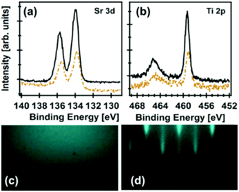 | ||
Fig. 5 X-ray photoelectron spectra of (a) Sr 3d and (b) Ti 2p after 36 subcycles (∼2 nm STO (dashed brown line)), and after 155 subcycles (∼8 nm STO (solid black line)); RHEED images after depositing an 8 nm STO film before (c) and after annealing (d) at 650 °C for 1 h; a deposition temperature of 225 °C with a Sr![[thin space (1/6-em)]](https://www.rsc.org/images/entities/char_2009.gif) :Ti 2:1 subcycle ratio for the subsequent STO film; Copyright WileyVCH Verlag GmbH & Co. KGaA. Reproduced with permission from ref. 117. :Ti 2:1 subcycle ratio for the subsequent STO film; Copyright WileyVCH Verlag GmbH & Co. KGaA. Reproduced with permission from ref. 117. | ||
In contrast to XPS, Rutherford backscattering spectrometry (RBS) is usually used to measure the bulk composition of the film. In addition to the composition and relative concentration, it also provides information on the sample depth, electron density, as well as the crystal structure and lattice damage in crystalline samples. The Niinistö group of the University of Helsinki has used RBS and time-of-flight elastic recoil detection analysis (TOF-ERDA) to precisely measure and tune the composition and thickness of PbTiO3,139 PbZrO3,123 and STO98 to investigate the effect of the precursor, chamber temperature, and sub-cycle ratio on the composition and post-processing crystallization behavior upon high-temperature annealing. Spectroscopic ellipsometry is the most common approach to determine the thickness of perovskite thin films. However, the correctness of the optical model for multicomponent films usually requires validation by means of cross-sectional transmission electron microscopy (TEM) and TEM-Energy dispersive spectroscopy (EDS).83,86,87 For non-planar substrates, TEM-EDS and TEM elemental energy loss spectroscopy (TEM-EELS) are emerging approaches to measure the thickness and compositional step coverage. The Hwang group of Seoul National University used TEM-EDS to investigate cross-sectional images of a SiO2 high-aspect-ratio structure with a ∼100 nm diameter opening and a depth of ∼1 μm coated with ∼8–9.5 nm thick ALD STO. The insight provided by this type of characterization played a key role in the development of suitable Sr precursors to coat high-aspect-ratio structures for DRAM applications.79,121 The thickness and compositional step coverages of up to ∼85% (bottom thickness/top thickness)115 and of 95% (Sr/(Sr + Ti)bottom/Sr/(Sr + Ti)top)79 were achieved (Fig. 6(a)). The Prinz group of Stanford University recently reported the coverage of a non-planar SiO2 structure with BaO, a promising finding for the future deposition of high-k BTO on high-aspect-ratio substrates.106
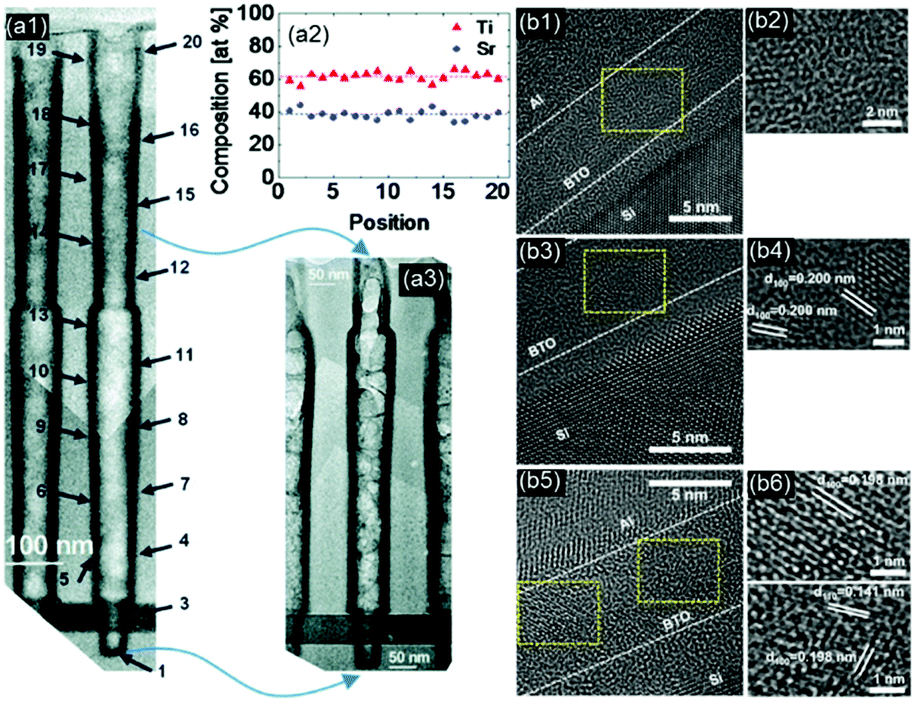 | ||
| Fig. 6 (a1–a3) Cross-sectional TEM and EDS results showing conformal thickness and composition step coverage (>95%) of an STO film inside a capacitor hole structure, reprinted with permission from ref. 79. Copyright (2011) American Chemical Society; (b1, b3 and b5) as-deposited, 1 and 3 h O2-plasma-treated BTO films, respectively, (b2, b4 and b6) zoomed-in images of the yellow boxes in b1, b3 and b5, respectively, reprinted with permission from ref. 64. Copyright (2014) American Chemical Society. | ||
For investigating the crystal structure after annealing the film, XRD is by far the most widely used technique. Due to interfacial and lattice constraints and compositional inhomogeneity, ultrathin films are usually largely distorted from the ideal cubic crystal structure. Moreover, the high dielectric constant achieved for stoichiometric films gives rise to high leakage currents. Al-doping and compositional variations seem to suppress leakage current densities at the expense of capacitance.64,137 Due to these expected large deviations from the ideal perovskite crystal, TEM analysis has been performed to explore the bulk morphology of a BTO film annealed in O2 plasma.64,90 They discovered that crystalline grains grow with increasing plasma treatment duration, as shown in Fig. 6(b). The lattice spacing in the crystalline area of the film corresponds well to the (100) and (110) directions of cubic, tetragonal, or rhombohedral BTO.
The same group recently employed the synchrotron-based X-ray absorption near edge structure (XANES) to investigate the atomic structure of BTO films with different compositions, post-process annealing strategies and underlying substrates.108 Analyzing the O K-edge, they gave several atomic scale explanations for the electrical and morphological properties of ultrathin-film BTO. For example, the binary metal-oxide constituents BaO and TiO2 mix to form continuous BTO during the deposition already. Furthermore, the increase in the leakage current with the Ti content was explained by the shift of the O2p–Ti3d hybridized states to a lower energy with increasing Ti content. This lowers the band gap of the film.
4. Conclusions
In this paper, we discussed the properties of high-k perovskite oxides prepared using the ALD process. In particular, we focused on the relation between electrical properties and the ALD process conditions with particular emphasis on the perovskites SrTiO3 (STO) and BaTiO3 (BTO). We discussed a variety of methods to achieve a high k value by changing the phase and overcoming the degradation effects such as leakage currents by reducing the micro-cracks and defects. We first discussed the effects of in-cycle annealing (ICA) and post deposition annealing (PDA) leading to the crystallization of the perovskite thin films. Short and high temperature ICA, required for a high throughput process, is not desirable as it necessitates rapid heating and cooling steps between the ALD cycles. Bypassing these high temperature requirements, the flash-lamp annealing (FLA-ALD) process has been developed. In addition, PDA was extensively studied and optimized to create high-quality STO and BTO films with desired cubic crystal phases. Though dielectric constants as high as 200 were achievable for ALD STO and BTO, these films exhibited relatively high leakage currents due to the inclusion of cracks induced by large crystalline grains. Studies on compositional variations revealed that a relative enrichment of A-site cations (Ba, Sr) allows high k values while preserving low leakage currents. This strongly influences the crystallization temperature and texture of the crystallized samples. Plasma treatments have also been addressed as a solution to achieve the desired crystal phase and dielectric properties, overcoming crack formation and related drawbacks in leakage currents and film damage. Direct plasma applied at a close distance to the substrates causes a high flux of accelerated ions with high kinetic energy, sufficient to rearrange film ions in the desired order. In general, remote plasma generates a comparably low density and low flux of ions energetically insufficient to fully crystallize films. However, there are few reports on the successful fabrication of partly crystalline BTO films using remote plasma treatment. This strategy seems to be promising to precisely tailor the film crystallinity. Most of the plasma treatments were conducted by an intra-deposition process, which has proven to be more effective compared to post-deposition treatments. Seed layering is also a well-established strategy for crystallizing ALD films. It consists of layering an extremely thin crystalline seed layer (usually <5 nm thick) prior to the deposition of ALD perovskites. Most reported uses of this method have been applied for ALD STO using seed layers of STO and SrO. This way, k values as high as ∼160 have been achieved on Ru substrates forming a RuO2 interlayer beneath the SrO seed layer. An improvement in the capacitance is another observed effect of using the annealed seed layers. The development of thermally stable and chemically active precursors is also crucial for developing high k ALD perovskite films. Precursors stable at high temperature and/or high-energy plasma are pivotal for crystallizing films.Ti and Sr compounds with β-diketonates (tmhd = tetramethylheptanedione) are processable up to ∼400 °C. STO can therefore be synthesized at 370 °C. However, decomposition and low volatility make these precursors impractical in an industrial setting. Cp (cyclopentadienyl) precursors, in contrast, are stable against thermal composition and exhibit high vapor pressure increasing their use in research and industry. With recent developments, deposition temperatures of up to 370 °C for STO are possible. These compounds seem also promising for depositing BTO; however, difficulties in terms of self-limiting behavior remain, potentially favoring the development of alternatives.
Thin film perovskites hold a lot of promise; however, they are complex functional materials and challenging to synthesize and understand. Their electrical properties, e.g. their dielectric constants, heavily depend on their morphology, their crystal structure and composition influenced by thickness, atomic arrangement, substrate and homogeneity. It is crucial to find reliable and repeatable processing solutions for ALD perovskites, for which, we have to fully characterize the obtained ultrathin films and link it to the ALD process. Research on fabrication goes hand in hand with the development of novel characterization methods and tools. Our review therefore presents innovative approaches that already shed new light on morphology and composition of thin film perovskites further establishing a closed loop desired between dielectric material properties and ALD processing strategies and conditions.
Acknowledgements
This research was supported by the LG Yonam Foundation, the National Research Foundation of Korea grant funded by the Korea government (NRF-2016R1D1A1B03932377), Human Resources Program in Energy Technology of the Korea Institute of Energy Technology Evaluation and Planning (KETEP), which received financial resources from the Ministry of Trade, Industry & Energy, Republic of Korea (no. 20144010200770) and the Korea University Internal Grant. The Brain Korea 21 Plus program (21A20131712520) is also acknowledged for its support. J. T. acknowledges funding from the Austrian Research fund under contract J3505-N20. J. A. acknowledges the financial support from the National Research Foundation under the Ministry of Education, Korea (NRF-2015R1D1A1A01058963). The authors thank Prof. Rick Reis who assisted with editing the manuscript.References
- S. Zaitsu, S. Motokoshi, T. Jitsuno, M. Nakatsuka and T. Yamanaka, Jpn. J. Appl. Phys., 2002, 41, 160 CrossRef CAS.
- T. Suntola, Thin Solid Films, 1992, 216, 84 CrossRef CAS.
- J. An, Y.-B. Kim and F. B. Prinz, Phys. Chem. Chem. Phys., 2013, 15, 7520 RSC.
- R. M. Costescu, D. G. Cahill, F. H. Fabreguette, Z. A. Sechrist and S. M. George, Science, 2004, 303, 989 CrossRef CAS PubMed.
- R. G. Gordon, D. Hausmann, E. Kim and J. Shepard, Chem. Vap. Deposition, 2003, 9, 73 CrossRef CAS.
- N. P. Dasgupta, H. J. Jung, O. Trejo, M. T. McDowell, A. Hryciw, M. Brongersma, R. Sinclair and F. B. Prinz, Nano Lett., 2011, 11, 934 CrossRef CAS PubMed.
- J. W. Kim, B. Kim, S. W. Park, W. Kim and J. H. Shim, Nanotechnology, 2014, 25, 435 Search PubMed.
- S. W. Park, J. W. Kim, H. J. Choi and J. H. Shim, J. Vac. Sci. Technol., A, 2014, 32, 01A115 Search PubMed.
- Y. K. Li, H. J. Choi, H. K. Kim, N. K. Chean, M. Kim, J. Koo, H. J. Jeong, D. Y. Jang and J. H. Shim, J. Power Sources, 2015, 295, 175 CrossRef CAS.
- C. Marichy, M. Bechelany and N. Pinna, Adv. Mater., 2012, 24, 1017 CrossRef CAS PubMed.
- C. C. Chao, J. S. Park, X. Tian, J. H. Shim, T. M. Gür and F. B. Prinz, ACS Nano, 2013, 7, 2186 CrossRef CAS PubMed.
- M. Groner, F. Fabreguette, J. Elam and S. George, Chem. Mater., 2004, 16, 639 CrossRef CAS.
- G. B. Lee, K. S. Son, S. W. Park, J. H. Shim and B.-H. Choi, J. Vac. Sci. Technol., A, 2013, 31, 01A129 Search PubMed.
- A. H. Brozena, C. J. Oldham and G. N. Parsons, J. Vac. Sci. Technol., A, 2016, 34, 010801 Search PubMed.
- S. W. Lee, O. S. Kwon, J. H. Han and C. S. Hwang, Appl. Phys. Lett., 2008, 92, 222903 CrossRef.
- T. Suntola, Mater. Sci. Rep., 1989, 4, 261 CrossRef CAS.
- M. Leskelä and M. Ritala, J. Phys. IV, 1995, 5, C5 CrossRef.
- L. Niinistö, M. Ritala and M. Leskelä, Mater. Sci. Eng., 1996, 41, 23 CrossRef.
- S. George, A. Ott and J. Klaus, J. Phys. Chem., 1996, 100, 13121 CrossRef CAS.
- M. Ritala and M. Leskelä, Nanotechnology, 1999, 10, 19 CrossRef CAS.
- M. Leskelä and M. Ritala, Thin Solid Films, 2002, 409, 138 CrossRef.
- M. Leskelä and M. Ritala, Angew. Chem., Int. Ed., 2003, 42, 5548 CrossRef PubMed.
- H. Kim, J. Vac. Sci. Technol., B: Microelectron. Nanometer Struct. – Process., Meas., Phenom., 2003, 21, 2231 CrossRef CAS.
- L. Niinistö, M. Nieminen, J. Päiväsaari, J. Niinistö and M. Putkonen, Phys. Status Solidi A, 2004, 201, 1443 CrossRef.
- R. L. Puurunen, J. Appl. Phys., 2005, 97, 121301 CrossRef.
- M. Knez, K. Nielsch and L. Niinistö, Adv. Mater., 2007, 19, 3425 CrossRef CAS.
- H. Kim, H.-B.-R. Lee and W. J. Maeng, Thin Solid Films, 2009, 517, 2563 CrossRef CAS.
- S. M. George, Chem. Rev., 2010, 110, 111 CrossRef CAS PubMed.
- N. Pinna and M. Knez, Atomic layer deposition of nanostructured materials, John Wiley & Sons, 2012 Search PubMed.
- ITRS, International technology roadmap for semiconductors, 2013.
- M. Kessel, R. A. De Souza and M. Martin, Phys. Chem. Chem. Phys., 2015, 17, 12587 RSC.
- A. Von Hippel, Rev. Mod. Phys., 1950, 22, 221 CrossRef CAS.
- W. Heywang, J. Am. Ceram. Soc., 1964, 47, 484 CrossRef CAS.
- R. Perez-Casero, J. Perriere, A. Gutierrez-Llorente, D. Defourneau, E. Millon, W. Seiler and L. Soriano, Phys. Rev. B: Condens. Matter Mater. Phys., 2007, 75, 165317 CrossRef.
- G. Jonker and J. Van Santen, Physica, 1953, 19, 120 CrossRef CAS.
- J. G. Bednorz and K. A. Müller, Rev. Mod. Phys., 1988, 60, 585 CrossRef CAS.
- C. Ahn, K. Rabe and J.-M. Triscone, Science, 2004, 303, 488 CrossRef CAS PubMed.
- G. Catalan and J. F. Scott, Adv. Mater., 2009, 21, 2463 CrossRef CAS.
- J.-G. Cheng, J.-S. Zhou, J. Goodenough and C.-Q. Jin, Phys. Rev. B: Condens. Matter Mater. Phys., 2012, 85, 184430 CrossRef.
- S. Dong and J.-M. Liu, Mod. Phys. Lett. B, 2012, 26, 1230004 CrossRef.
- N. Nuraje and K. Su, Nanoscale, 2013, 5, 8752 RSC.
- M. D. McDaniel, T. Q. Ngo, S. Hu, A. Posadas, A. A. Demkov and J. G. Ekerdt, Appl. Phys. Rev., 2015, 2, 041301 Search PubMed.
- R. E. Cohen, Nature, 1992, 358, 136 CrossRef CAS.
- R. Ulrich, L. Schaper, D. Nelms and M. Leftwich, Int. J. Microcircuits Electron. Packag., 2000, 23, 172 CAS.
- J. Kittl, K. Opsomer, M. Popovici, N. Menou, B. Kaczer, X. Wang, C. Adelmann, M. Pawlak, K. Tomida and A. Rothschild, Microelectron. Eng., 2009, 86, 1789 CrossRef CAS.
- J. Niinistö, K. Kukli, M. Heikkilä, M. Ritala and M. Leskelä, Adv. Eng. Mater., 2009, 11, 223 CrossRef.
- S. K. Kim, W.-D. Kim, K.-M. Kim, C. S. Hwang and J. Jeong, Appl. Phys. Lett., 2004, 85, 4112 CrossRef CAS.
- B. Choudhury, K. Rao and R. Choudhury, J. Mater. Sci., 1989, 24, 3469 CrossRef CAS.
- P. K. Dutta, R. Asiaie, S. A. Akbar and W. Zhu, Chem. Mater., 1994, 6, 1542 CrossRef CAS.
- G. Arlt and D. Hennings, J. Appl. Phys., 1985, 58, 1619 CrossRef CAS.
- W. Chang and L. Sengupta, J. Appl. Phys., 2002, 92, 3941 CrossRef CAS.
- P. K. Chu, Croatia, INTECH, 2010 Search PubMed.
- J. Junquera and P. Ghosez, Nature, 2003, 422, 506 CrossRef CAS PubMed.
- L. H. Parker and A. F. Tasch, IEEE Circuits Devices Mag., 1990, 6, 17 CrossRef.
- S. M. Aygün, J. F. Ihlefeld, W. J. Borland and J.-P. Maria, J. Appl. Phys., 2011, 109, 034108 CrossRef.
- T. Shaw, S. Trolier-McKinstry and P. McIntyre, Annu. Rev. Mater. Sci., 2000, 30, 263 CrossRef CAS.
- M. Stengel and N. A. Spaldin, Nature, 2006, 443, 679 CrossRef CAS PubMed.
- L. Ni, X. Chen, X. Liu and R. Hou, Solid State Commun., 2006, 139, 45 CrossRef CAS.
- H. T. Langhammer, T. Müller and K.-H. Felgner, and H.-P. Abicht, J. Am. Ceram. Soc., 2000, 83, 605 CrossRef CAS.
- S. K. Dey and J. J. Lee, IEEE Trans. Electron Devices, 1992, 39, 1607–1613 CrossRef CAS.
- P.-Y. Chen, C.-S. Chen, C.-S. Tu, C.-D. Cheng and J.-S. Cherng, Ceram. Int., 2014, 40, 6137 CrossRef CAS.
- D. S. Boesch, J. Son, J. M. LeBeau and J. Cagnon, and S. Stemmer, Appl. Phys. Express, 2008, 1, 091602 CrossRef.
- S. P. Senanayak, B. Yang, T. H. Thomas, N. Giesbrecht, W. Huang, E. Gann, B. Nair, K. Goedel, S. Guha, X. Moya, C. R. McNeill, P. Docampo, A. Sadhanala, R. H. Friend and H. Sirringhaus, Sci. Adv., 2017, 3, e1601935 CrossRef PubMed.
- J. An, T. Usui, M. Logar, J. Park, D. Thian, S. Kim, K. Kim and F. B. Prinz, ACS Appl. Mater. Interfaces, 2014, 6, 10656 CAS.
- S. J. Billinge and I. Levin, Science, 2007, 316, 561 CrossRef CAS PubMed.
- M. Vehkamäki, T. Hatanpää, M. Ritala, M. Leskelä, S. Väyrynen and E. Rauhala, Chem. Vap. Deposition, 2007, 13, 239 CrossRef.
- M. C. Langston, N. P. Dasgupta, H. J. Jung, M. Logar, Y. Huang, R. Sinclair and F. B. Prinz, J. Phys. Chem. C, 2012, 116, 24177 CAS.
- R. McMahon, M. Smith, K. Seffen, M. Voelskow, W. Anwand and W. Skorupa, Vacuum, 2007, 81, 1301 CrossRef CAS.
- S. Raoux, Phase Change Materials, Springer, 2009, p. 99 Search PubMed.
- M. Vehkamäki, T. Hatanpää, T. Hänninen, M. Ritala and M. Leskelä, Electrochem. Solid-State Lett., 1999, 2, 504 CrossRef.
- N. Aslam, V. Longo, W. Keuning, F. Roozeboom, W. Kessels, R. Waser and S. Hoffmann-Eifert, Phys. Status Solidi A, 2014, 211, 389 CrossRef CAS.
- M. A. Pawlak, B. Kaczer, M. S. Kim, M. Popovici, K. Tomida, J. Swerts, K. Opsomer, W. Polspoel, P. Favia, C. Vrancken, C. Demeurisse, W. C. Wang, V. V. Afanas’ev, W. Vandervorst, H. Bender, I. Debusschere, L. Altimime and J. A. Kittl, Appl. Phys. Lett., 2010, 97, 162906 CrossRef.
- N. Menou, M. Popovici, S. Clima, K. Opsomer, W. Polspoel, B. Kaczer, G. Rampelberg, K. Tomida, M. Pawlak and C. Detavernier, J. Appl. Phys., 2009, 106, 094101 CrossRef.
- M. Pawlak, J. Swerts, M. Popovici, B. Kaczer, M.-S. Kim, W.-C. Wang, K. Tomida, B. Govoreanu, J. Delmotte and V. Afanasc'ev, Appl. Phys. Lett., 2012, 101, 042901 CrossRef.
- M. Pawlak, B. Kaczer, M.-S. Kim, M. Popovici, J. Swerts, W.-C. Wang, K. Opsomer, P. Favia, K. Tomida and A. Belmonte, Appl. Phys. Lett., 2011, 98, 182902 CrossRef.
- R. Matero, A. Rahtu, S. Haukka, M. Tuominen, M. Vehkamäki, T. Hatanpää, M. Ritala and M. Leskelä, ECS Trans., 2006, 1, 137 CAS.
- P. Schindler, M. Logar, J. Provine and F. B. Prinz, Langmuir, 2015, 31, 5057 CrossRef CAS PubMed.
- V. Longo, N. Leick, F. Roozeboom and W. Kessels, ECS J. Solid State Sci. Technol., 2013, 2, N15 CrossRef CAS.
- S. W. Lee, J. H. Han, S. Han, W. Lee, J. H. Jang, M. Seo, S. K. Kim, C. Dussarrat, J. Gatineau, Y. S. Min and C. S. Hwang, Chem. Mater., 2011, 23, 2227 CrossRef CAS.
- W. Lee, J. H. Han, W. Jeon, Y. W. Yoo, S. W. Lee, S. K. Kim, C.-H. Ko, C. Lansalot-Matras and C. S. Hwang, Chem. Mater., 2013, 25, 953 CrossRef CAS.
- D. S. Kil, J. M. Lee and J. S. Roh, Chem. Vap. Deposition, 2002, 8, 195 CrossRef CAS.
- J. Lee, Y. Cho, Y. Min, D. Kim and S. Rhee, J. Vac. Sci. Technol., A, 2002, 20, 1828 CAS.
- O. S. Kwon, S. K. Kim, M. Cho, C. S. Hwang and J. Jeong, J. Electrochem. Soc., 2005, 152, C229 CrossRef CAS.
- S. W. Lee, O. S. Kwon and C. S. Hwang, Microelectron. Eng., 2005, 80, 158 CrossRef CAS.
- J.-Y. Kim, J.-H. Ahn, S.-W. Kang, J.-H. Kim and J.-S. Roh, Appl. Phys. Lett., 2007, 91, 092910 CrossRef.
- O. S. Kwon, S. W. Lee, J. H. Han and C. S. Hwang, J. Electrochem. Soc., 2007, 154, G127 CrossRef CAS.
- J.-H. Ahn, S.-W. Kang, J.-Y. Kim, J.-H. Kim and J.-S. Roh, J. Electrochem. Soc., 2008, 155, G185 CrossRef CAS.
- J.-H. Ahn, J.-Y. Kim, J.-H. Kim, J.-S. Roh and S.-W. Kang, Electrochem. Solid-State Lett., 2009, 12, G5 CrossRef CAS.
- V. Longo, N. Leick, F. Roozeboom and W. Kessels, ECS Trans., 2011, 41, 63 CAS.
- E. Langereis, R. Roijmans, F. Roozeboom, M. C. M. van de Sanden and W. M. M. Kessels, J. Electrochem. Soc., 2011, 158, G34 CrossRef CAS.
- C. Yim, S. Kim, Y. Kang, M.-H. Cho and D.-H. Ko, Electrochem. Solid-State Lett., 2011, 14, G45 CrossRef CAS.
- V. Longo, M. Verheijen, F. Roozeboom and W. Kessels, ECS J. Solid State Sci. Technol., 2013, 2, N120 CrossRef CAS.
- P. Schindler, Y. Kim, D. Thian, J. An and F. B. Prinz, Scr. Mater., 2016, 111, 106 CrossRef CAS.
- S. W. Lee, J. H. Han, O. S. Kwon and C. S. Hwang, J. Electrochem. Soc., 2008, 155, G253 CrossRef CAS.
- N. Menou, M. Popovici, K. Opsomer, B. Kaczer, M. A. Pawlak, C. Adelmann, A. Franquet, P. Favia, H. Bender and C. Detavernier, Jpn. J. Appl. Phys., 2010, 49, 04DD01 CrossRef.
- M. Popovici, K. Tomida, J. Swerts, P. Favia, A. Delabie, H. Bender, C. Adelmann, H. Tielens, B. Brijs and B. Kaczer, Phys. Status Solidi A, 2011, 208, 1920 CrossRef CAS.
- O. Nilsen, E. Rauwel, H. Fjellvåg and A. Kjekshus, J. Mater. Chem., 2007, 17, 1466 RSC.
- A. Kosola, M. Putkonen, L.-S. Johansson and L. Niinistö, Appl. Surf. Sci., 2003, 211, 102 CrossRef CAS.
- T. P. Holme and F. B. Prinz, J. Phys. Chem. A, 2007, 111, 8147 CrossRef CAS PubMed.
- K. Endo and T. Tatsumi, Jpn. J. Appl. Phys., 2003, 42, L685 CrossRef CAS.
- B. Miao, R. Mahapatra, N. Wright and A. Horsfall, J. Appl. Phys., 2008, 104, 054510 CrossRef.
- R. Katamreddy, Z. Wang, V. Omarjee, P. V. Rao, C. Dussarrat and N. Blasco, ECS Trans., 2009, 25, 217 CAS.
- H. J. Choi, S. W. Park, G. D. Han, J. Na, G.-T. Kim and J. H. Shim, Appl. Phys. Lett., 2014, 104, 242105 CrossRef.
- J. H. Shim, J. S. Park, J. An, T. M. Gür, S. Kang and F. B. Prinz, Chem. Mater., 2009, 21, 3290 CrossRef CAS.
- T. Hatanpää, M. Vehkamäki, I. Mutikainen, J. Kansikas, M. Ritala and M. Leskelä, Dalton Trans., 2004, 1181 RSC.
- S. Acharya, J. Torgersen, Y. Kim, J. Park, P. Schindler, A. L. Dadlani, M. Winterkorn, S. Xu, S. P. Walch, T. Usui, C. Schildknecht and F. B. Prinz, J. Mater. Chem. C, 2016, 4, 1945 RSC.
- J. Im, S. Streiffer, O. Auciello and A. R. Krauss, Appl. Phys. Lett., 2000, 77, 2593 CrossRef CAS.
- J. Torgersen, S. Acharya, A. L. Dadlani, I. Petousis, Y. Kim, O. Trejo, D. Nordlund and F. B. Prinz, J. Phys. Chem. Lett., 2016, 7, 1428 CrossRef CAS PubMed.
- J. H. Choi, F. Zhang, Y.-C. Perng and J. P. Chang, J. Vac. Sci. Technol., B: Nanotechnol. Microelectron.: Mater., Process., Meas., Phenom., 2013, 31, 012207 Search PubMed.
- T. Watanabe, S. Hoffmann-Eifert, S. Mi, C. Jia, R. Waser and C. S. Hwang, J. Appl. Phys., 2007, 101, 014114 CrossRef.
- S. Riedel, J. Neidhardt, S. Jansen, L. Wilde, J. Sundqvist, E. Erben, S. Teichert and A. Michaelis, J. Appl. Phys., 2011, 109, 094101 CrossRef.
- J. An, Y. B. Kim, J. S. Park, J. H. Shim, T. M. Gür and F. B. Prinz, J. Vac. Sci. Technol., A, 2012, 30, 01A161 Search PubMed.
- T. P. Holme, C. Lee and F. B. Prinz, Solid State Ionics, 2008, 179, 1540 CrossRef CAS.
- T. Watanabe, S. Hoffmann-Eifert, F. Peter, S. Mi, C. Jia, C. S. Hwang and R. Waser, J. Electrochem. Soc., 2007, 154, G262 CrossRef CAS.
- W. Lee, W. Jeon, C. H. An, M. J. Chung, H. J. Kim, T. Eom, S. M. George, B. K. Park, J. H. Han and C. G. Kim, Chem. Mater., 2015, 27, 3881 CrossRef CAS.
- W. Lee, S. Yoo, W. Jeon, Y. W. Yoo, C. H. An, M. J. Chung, H. J. Kim, S. W. Lee and C. S. Hwang, Thin Solid Films, 2015, 589, 723 CrossRef CAS.
- M. D. McDaniel, T. Q. Ngo, A. Posadas, C. Hu, S. Lu, D. J. Smith, E. T. Yu, A. A. Demkov and J. G. Ekerdt, Adv. Mater. Interfaces, 2014, 1, 1400081 CrossRef.
- M. D. McDaniel, C. Hu, S. Lu, T. Q. Ngo, A. Posadas, A. Jiang, D. J. Smith, T. Y. Edward, A. A. Demkov and J. G. Ekerdt, J. Appl. Phys., 2015, 117, 054101 CrossRef.
- M. D. McDaniel, A. Posadas, T. Q. Ngo, A. Dhamdhere, D. J. Smith, A. A. Demkov and J. G. Ekerdt, J. Vac. Sci. Technol., A, 2013, 31, 01A136 Search PubMed.
- T. Q. Ngo, A. B. Posadas, M. D. McDaniel, C. Hu, J. Bruley, T. Y. Edward, A. A. Demkov and J. G. Ekerdt, Appl. Phys. Lett., 2014, 104, 082910 CrossRef.
- J. H. Han, W. Lee, W. Jeon, S. W. Lee, C. S. Hwang, C. Ko and J. Gatineau, Chem. Mater., 2012, 24, 4686 CrossRef CAS.
- S. W. Lee, J. H. Han and C. S. Hwang, Electrochem. Solid-State Lett., 2009, 12, G69 CrossRef CAS.
- J. Harjuoja, S. Väyrynen, M. Putkonen, L. Niinistö and E. Rauhala, Appl. Surf. Sci., 2007, 253, 5228 CrossRef CAS.
- M. Lie, O. Nilsen, H. Fjellvåg and A. Kjekshus, Dalton Trans., 2009, 481 RSC.
- H. J. Lee, G. W. Hwang, K. Lee, G. H. Kim and C. S. Hwang, Presented in part at the 2007 Sixteenth IEEE International Symposium on the Applications of Ferroelectrics, 2007.
- M. Vehkamäki, T. Hänninen, M. Ritala, M. Leskelä, T. Sajavaara, E. Rauhala and J. Keinonen, Chem. Vap. Deposition, 2001, 7, 75 CrossRef.
- H. García, H. Castán, A. Gómez, S. Dueñas, L. Bailón, K. Kukli, M. Kariniemi, M. Kemell, J. Niinistö and M. Ritala, J. Vac. Sci. Technol., B: Nanotechnol. Microelectron.: Mater., Process., Meas., Phenom., 2011, 29, 01AC04 Search PubMed.
- J.-H. Kim, J.-Y. Kim and S.-W. Kang, J. Appl. Phys., 2005, 97, 093505 CrossRef.
- T. Blomberg, J. Anttila, S. Haukka, M. Tuominen, M. Lukosius, C. Wenger and T. Saukkonen, Thin Solid Films, 2012, 520, 6535 CrossRef CAS.
- K. Kukli, M. Ritala, T. Sajavaara, T. Hänninen and M. Leskelä, Thin Solid Films, 2006, 500, 322 CrossRef CAS.
- K. Black, M. Werner, R. Rowlands–Jones, P. R. Chalker and M. J. Rosseinsky, Chem. Mater., 2011, 23, 2518 CrossRef CAS.
- M. Lukosius, C. Wenger, T. Blomberg, A. Abrutis, G. Lupina, P. Baumann and G. Ruhl, ECS J. Solid State Sci. Technol., 2012, 1, N1 CrossRef CAS.
- M. D. McDaniel, A. Posadas, T. Q. Ngo, C. M. Karako, J. Bruley, M. M. Frank, V. Narayanan, A. A. Demkov and J. G. Ekerdt, J. Appl. Phys., 2014, 115, 224108 CrossRef.
- M. Popovici, S. Van Elshocht, N. Menou, P. Favia, H. Bender, E. Rosseel, J. Swerts, C. Adelmann, C. Vrancken, A. Moussa, H. Tielens, K. Tomida, M. Pawlak, B. Kaczer, G. Schoofs, W. Vandervorst, D. J. Wouters and J. A. Kittl, J. Vac. Sci. Technol., B: Nanotechnol. Microelectron.: Mater., Process., Meas., Phenom., 2011, 29, 01A304 Search PubMed.
- F. Zhang, Y.-C. Perng, J. H. Choi, T. Wu, T.-K. Chung, G. P. Carman, C. Locke, S. Thomas, S. E. Saddow and J. P. Chang, J. Appl. Phys., 2011, 109, 124109 CrossRef.
- T. Watanabe, S. Hoffmann-Eifert, C. S. Hwang and R. Waser, J. Electrochem. Soc., 2008, 155, D715 CrossRef CAS.
- Y. W. Yoo, W. Jeon, W. Lee, C. H. An, S. K. Kim and C. S. Hwang, ACS Appl. Mater. Interfaces, 2014, 6, 22474 CAS.
- R. Katamreddy, V. Omarjee, B. Feist, C. Dussarrat, M. Singh and C. Takoudis, ECS Trans., 2008, 16, 487 CAS.
- J. Harjuoja, A. Kosola, M. Putkonen and L. Niinistö, Thin Solid Films, 2006, 496, 346 CrossRef CAS.
Footnote |
| † Equally contributed. |
| This journal is © The Royal Society of Chemistry 2017 |