
 Open Access Article
 This Open Access Article is licensed under a
 Creative Commons Attribution 3.0 Unported Licence
Understanding surface chemistry during MAPbI3 spray deposition and its effect on photovoltaic performance†
Conor
Rocks
 *a,
Vladimir
Svrcek
b,
Paul
Maguire
a and
Davide
Mariotti
*a
*a,
Vladimir
Svrcek
b,
Paul
Maguire
a and
Davide
Mariotti
*a
aNanotechnology & Integrated Bio-Engineering Centre (NIBEC), Ulster University, UK. E-mail: rocks-c2@email.ulster.ac.uk
bResearch Center for Photovoltaics, National Institute of Advanced Industrial Science and Technology (AIST), Central 2, Umezono 1-1-1, Tsukuba, 305-8568, Japan
First published on 3rd January 2017
Abstract
In recent years there has been significant research into organic–inorganic halide perovskites for photovoltaic applications and has resulted in power conversion efficiencies greater than 20%. A number of deposition techniques have been utilized to produce high quality perovskite films including thermal evaporation, single and two-step spin coating and vapor assisted processes. However, these laboratory based fabrication methods are not well matched with low costing, roll to roll processing that is associated with large scale manufacture. In this work we use a low costing and rapid spray coating technique to fabricate solution processed MAPbI3 films with controlled film thickness achieved through modifying concentration/spray volume. Investigation into the chemical composition and film morphology showed differing surface chemistries for the different film thicknesses, altering the surface morphology from large micro grained structures to small distorted grain arrangements. We have then implemented spray deposited films into solar devices (ITO/TiO2/MAPbI3/Au) and have studied the current density–voltage (JV) characteristics including light soaking effects. Through optimizing the absorber thickness the short-circuit current density is increased from 4.9 mA cm−2 to 22.3 mA cm−2, increasing overall power conversion efficiency by a factor >5. Investigation into the performance of devices under continued illumination showed an inverse relationship existed between low efficiency (thick) MAPbI3 films and high efficiency (thin) MAPbI3 films, where the former displayed large increases in overall performance compared to the rapid degradation in the latter. We attribute device instabilities to the increase in defect density as a consequence of the spray-induced surface chemistry, leading to trap assisted recombination at the back electrode.
Introduction
Over recent years, organic–inorganic halide perovskites have received considerable attention due to their intense light absorption, greater charge diffusion lengths and low exciton binding energies.1 Rapid developments in device engineering along with material processing have led to power conversion efficiencies greater than 20%.2,3 The perovskite structure is typically represented by the general formula ABX3, where in the case of organic–inorganic halide perovskites A is a small organic cation (CH3NH3+), B is a metal cation (Pb2+) and X is a monovalent halide anion (I−). Variations in the metal and halide components have been demonstrated to impact the perovskites electronic structure, enabling bandgap tunability between 1.5 eV and 3.1 eV.4 Despite the perovskites many enhanced opto-electronic properties, successful implementation into applications, mainly photovoltaic, has been hindered by a number of key operational issues. These issues arise from the complex nature of the perovskites intrinsic properties which are not yet fully understood. Under normal operating conditions, light soaking effects and hysteresis phenomena have been observed for perovskite solar cells.5–9 Experimental studies have shown that both light soaking effect and hysteresis phenomena are related to the electrode interfaces in heterojunction perovskite devices. There is a general consensus that a number of mechanisms may be responsible and act simultaneously, such as reorientation of ferroelectric organic cations,10 trapping/de-trapping of charge carriers,11 lattice distortion-induced polarization and ion migration.12,13 In order for perovskites enhanced properties to be successfully implemented into a range of applications, high quality thin films must be produced. Several deposition techniques including thermal evaporation,14 single and two step spin coating15,16 and vapor assisted processes17 have been optimized to achieve high quality perovskite films for use in high performing PV devices. However, these laboratory based fabrication methods for perovskite films are not well-matched with a low costing, roll to roll process that is typical for large scale manufacture.18 A solution would be to develop a one-step spray coating approach, which has already been successfully exploited for a range of electronic devices such as light emitting diodes,19 photo-detectors,20 field effect transistors21 and also photovoltaics.22,23 However, challenges still exist to deploy spray coating for perovskite photovoltaics as for instance thin layers as required for optimal device performance are still difficult to achieve by spray. Nonetheless, a one-step spray coating method still presents technological relevance and advantages that are highly beneficial to industrial manufacture, such as the ability to simultaneously provide high throughput, efficient use of material and uniform film coverage. Additionally, control over directional deposition means that grains grow in a vertically aligned manner, resulting in low number of grain boundaries that could benefit overall charge transport properties. A main issue concerning the implementation of methylammonium lead iodide (MAPbI3) as a feasible and efficient absorber for solar devices is its stability. Exposure to even ambient atmospheric conditions causes severe degradation of the MAPbI3 film and their unique opto-electronic properties diminish as a consequence. Numerous works have established the effects of moisture and oxygen ingress into MAPbI3 films and it is well understood that as MAI is evaporated solid PbI2 remains on the film, which turns into a yellowish shade from the original dark colour. MAI can be further broken down to CH3NH2 (liquid) and HI (liquid) with the latter easily reacting with O2 to form I2 (solid) and H2O (liquid) or decompose into I2 (solid) and H2 (gas).24 In this work we use a low costing and scalable one-step spray technique to fabricate solution processed MAPbI3 films. By changing the concentration of MAPbI3 in DMF solution (0.25 M and 0.125 M) along with the spray volume (400 μL, 300 μL and 200 μL) we were able to control the film thickness. The surface chemistry of MAPbI3 films induced during spraying are studied in detail using X-ray photoelectron spectroscopy (XPS) and indicates increased surface reactivity for reduced film thicknesses. A direct consequence is the accelerated decomposition from MAPbI3 to MAPbI2+x/PbI2 where we highlight in detail the intermediate chemical phases that are formed during this transition together with surface morphology changes. The spray deposited films are used in solar devices with TiO2 as an electron transfer/hole blocking layer and their current density–voltage (JV) characteristics are studied to include light soaking effects over a period of 0–6 min. This work provides in-depth details of changing surface chemistry as a result of the spray method, which highlights a more rapid degradation process at the surface of thinner films. The subsequent effect on the electronic band structure for spray produced MAPbI3 films is also analysed in details.Experimental section
Materials
Precursor materials triethanolamine, titanium(IV) isoperoxide and titanium(IV) oxide anatase nanopowder <25 nm diameter were purchased from Sigma-Aldrich and used as received. Methylammonium lead iodide (CH3NH3PbI3) perovskite powder with 99% purity was purchased from Xi’an p-OLED.Film deposition and device fabrication
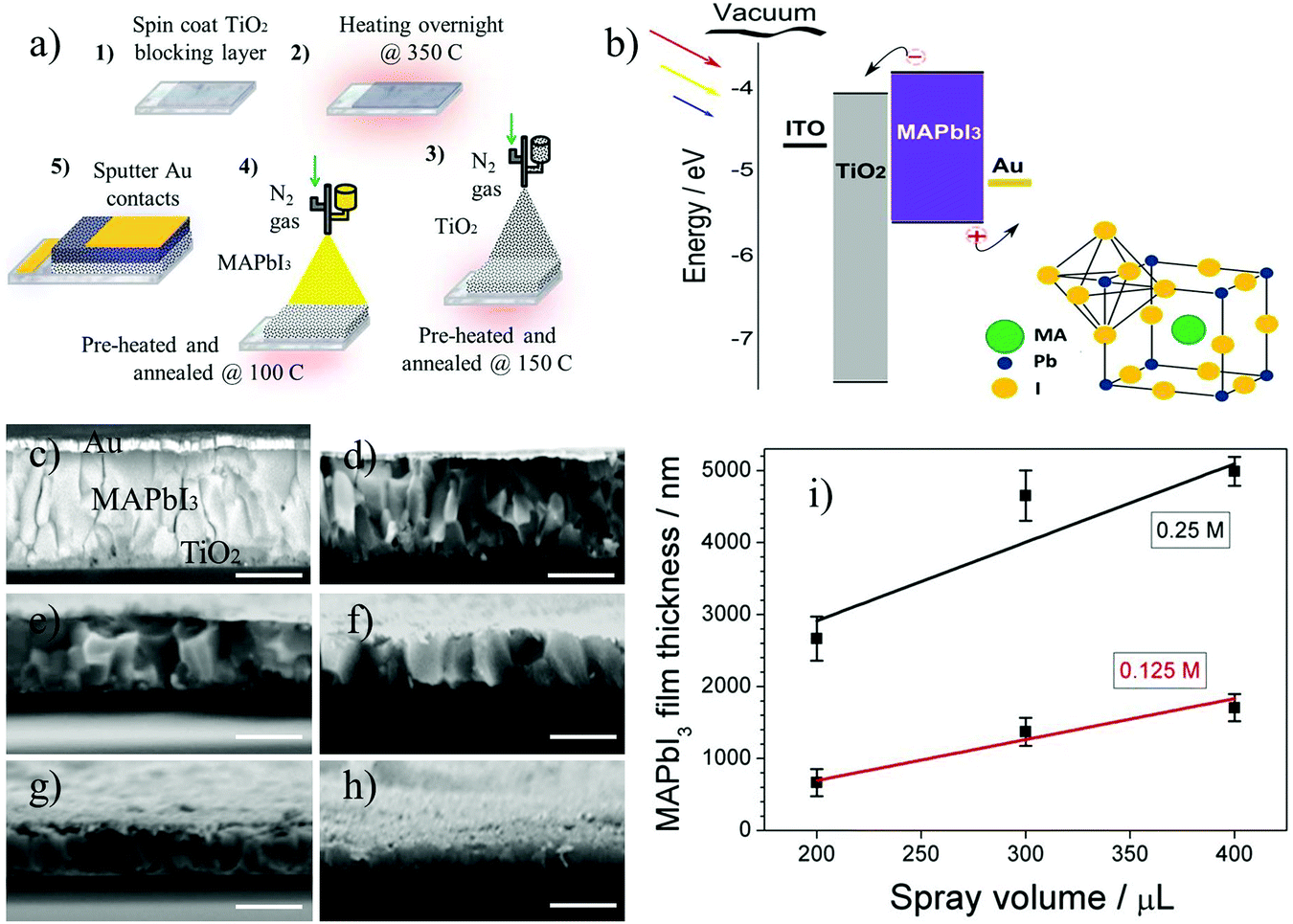 | ||
| Fig. 1 (a) Fabrication steps for the synthesis of MAPbI3 solar devices and (b) non-equilibrated band diagram for our cell architecture and (inset bottom right) unit cell for MAPbI3 perovskite. (c–h) Cross sectional scanning electron microscopy (SEM) images of deposited MAPbI3 on a mesoporous TiO2 layer by a one-step spray method using the following MAPbI3 in DMF concentration/spray volume: (c) 0.25 M/400 μL (d) 0.25 M/300 μL (e) 0.25 M/200 μL (f) 0.125 M/400 μL (g) 0.125 M/300 μL and (h) 0.125 M/200 μL. Scale bars 2.5 μm. (i) Measured MAPbI3 film thickness using following deposition implementing set concentrations and spray volumes. | ||
![[thin space (1/6-em)]](https://www.rsc.org/images/entities/char_2009.gif) :1) is mixed and sonicated for 30 minutes followed by an additional settling period of 30 minutes. 400 μL is then sprayed in air using an airbrush (pro series BD-132) via nitrogen gas flow at 1 bar pressure positioned 15 cm above a hot plate at 0° angle incident to substrate surface and annealed for 1 h at 150 °C to form a mesoporous TiO2 layer (Fig. 1a.3). Methylammonium lead iodide (CH3NH3PbI3) perovskite powder is mixed in dimethylformamide (DMF) at 60 °C at 0.25 M and 0.125 M (1 M = 0.619.9 g mL−1) and using the same spray deposition technique with nitrogen gas flow and at 1 bar pressure the solution is sprayed in air on to mesoporous TiO2 layer and annealed for 40 min at 100 °C (Fig. 1a.4). All samples were transferred directly to XPS vacuum chamber within minutes following the annealing procedure.
:1) is mixed and sonicated for 30 minutes followed by an additional settling period of 30 minutes. 400 μL is then sprayed in air using an airbrush (pro series BD-132) via nitrogen gas flow at 1 bar pressure positioned 15 cm above a hot plate at 0° angle incident to substrate surface and annealed for 1 h at 150 °C to form a mesoporous TiO2 layer (Fig. 1a.3). Methylammonium lead iodide (CH3NH3PbI3) perovskite powder is mixed in dimethylformamide (DMF) at 60 °C at 0.25 M and 0.125 M (1 M = 0.619.9 g mL−1) and using the same spray deposition technique with nitrogen gas flow and at 1 bar pressure the solution is sprayed in air on to mesoporous TiO2 layer and annealed for 40 min at 100 °C (Fig. 1a.4). All samples were transferred directly to XPS vacuum chamber within minutes following the annealing procedure.
Characterization of sprayed MAPbI3 films
Cross sectional scanning electron microscopy (SEM) was performed using a JEOL JSM-6010PLUS at 20 kV acceleration voltages. X-ray photoelectron spectroscopy (XPS) to determine surface chemical composition was performed using an X-ray source (Al = 1486 eV) and the Kratos AxisUltra DLD spectrometer with peak fitting performed using Kratos software. Current and voltage were 10 mA and 15 kV respectively with an operating pressure of 10−9 bar. Specific region scans were performed at a resolution of 0.05 eV and pass energy of 20 eV. X-ray spot size and hence capture area is equal to 400 μm2 with a penetration depth of 10 nm. Calibration of obtained spectra was performed using the C 1s peak located at 284.8 eV. Attenuated total reflectance Fourier transform infra-red spectroscopy (FTIR) was performed and measured using a Thermo-scientific spectrometer. Spectra were obtained over a range of 600–3500 cm−1 at a 2 cm−1 resolution. Raman spectroscopy was carried out using an ISA Lab-ram 300 confocal spectroscope with a 632.8 nm helium-neon laser to obtain spectra from 0 cm−1 to 500 cm−1 with 20 s exposure time and laser power of 10 mW. The Fermi level measurements are characterized using a scanning Kelvin probe system (KPTechnology) with a total of 20 measurements are taken across the sample surface and presented as a mean value with error bars representing standard deviation. Ultraviolet-visible (UV-Vis) absorption measurements are measured using a deuterium-halogen light source and an integrating sphere. Current density–voltage (JV) curves of devices incorporating sprayed MAPbI3 films were recorded by a Keithley 6430 sub-FA sourcemeter unit under illumination 1.5 AM in air at ambient temperature. The applied bias varied from −1 V to 1 V in steps of 0.01 V at a scan rate 700 mV s−1 consistently for all devices.Results
Varying MAPbI3 film thickness
MAPbI3 films of varying thickness were produced by changing concentration (0.25 M and 0.125 M) and spray volume (200 μL, 300 μL and 400 μL). To track the changes in film thickness the cross sectional scanning electron microscopy (SEM) images were taken (Fig. 1c–h). Fig. 1c image was captured using back scattered electrons and presented to differentiate between meso-TiO2/MAPbI3/Au layers. A number of measurements using a profilometer for compact TiO2 and mesoporous TiO2 show thicknesses of 32.76 nm ± 12.16 and 569.25 nm ± 145.02 nm respectively. A plot of film thickness versus spray volume for 0.25 M and 0.125 M concentrations of MAPbI3 in DMF show that film thickness decreases in a linear fashion with decreasing spray volume (Fig. 1i). Error bars represent 8 measurements taking across full width of film in order to highlight the homogeneousness nature of deposition process.Chemical analysis of MAPbI3 films
The XPS spectra were recorded to investigate the elemental composition and understand the impact that decreasing film thickness may factor into the surface stability and durability of our sprayed MAPbI3 films. The XPS survey spectrum (ESI†) for a typical MAPbI3 perovskite shows peaks at binding energies of 532 eV, 401 eV and 284.8 eV corresponding to the photoelectron peaks of O 1s, N 1s and C 1s respectively. The doublet peaks of I and Pb are located around 618 eV and 137 eV, respectively, with their associated spin orbit splitting. To assess the chemical changes of our MAPbI3 films produced at decreasing thicknesses, we recorded the high resolution photoelectron spectra of each sample. XPS spectra were calibrated to 284.8 eV according to the C 1s binding energy for adventitious (aliphatic) carbon.25 The core level spectra obtained were fitted using Gaussian line shapes after linear background subtraction. The atomic concentrations for each specific region were determined from the integrated area under their peaks accounting for photoionization cross section and plotted as a function of MAPbI3 film thickness (Fig. 2a); error bars in the y-axis represent average and standard deviation (SD) for 3 different spots across sample surface. There is a comparable reduction in the elemental composition for I 3d and N 1s components as the thickness of the MAPbI3 film reduces. The elemental composition for C 1s increases slightly whereas the Pb 4f component decreases by a similar amount, also with decreasing thickness. Most noticeably is the increase in O 1s concentration for decreasing MAPbI3 film thicknesses.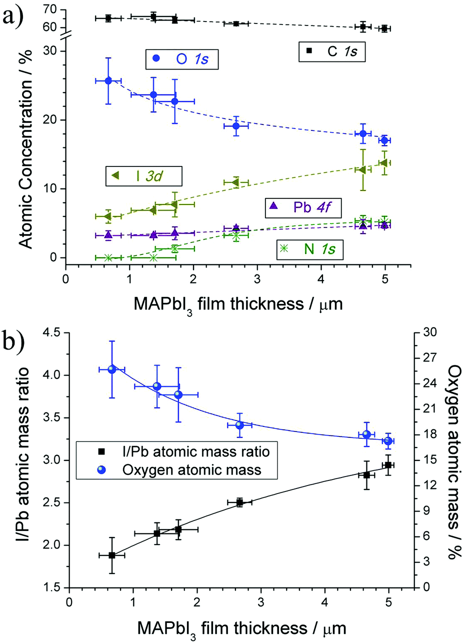 | ||
| Fig. 2 (a) Atomic concentration of C 1s, O 1s, N 1s, Pb 4f and I 3d components in MAPbI3 films as a function of film thickness, determined from XPS measurements with (b) quantified XPS results highlighting atomic mass ratio for I/Pb and oxygen atomic mass percentage for decreasing MAPbI3 film thickness. | ||
The atomic mass ratio of I/Pb and the total atomic mass percentage of O 1s vs. MAPbI3 film thickness, calculated from the integrated areas under Pb 4f, I 3d and O 1s peaks, show a mirrored symmetry (Fig. 2b). As highlighted previously, for decreasing MAPbI3 film thickness, the total atomic concentration of the I 3d peak decreased gradually relative to the total concentration of the Pb 4f peak. This reduction (we expect a 3:1 I/Pb ratio in the stoichiometric crystal) implies that the amount of surface oxygen species correlates directly with the decrease in iodide concentration for MAPbI3 films.
C 1s core level spectra for our MAPbI3 with I/Pb ratio closer to the stoichiometric 3:1 (i.e. thickness >2 μm, Fig. 2b) included three peaks located at 284.8 eV, 285.9 eV and 287 eV (Fig. 3a–c). The peak found at 284.8 eV is commonly used for calibration and is known as adventitious carbon or adsorbed surface hydrocarbon species from the atmosphere.25 The peak located at 285.9 eV can be attributed to methyl carbons in the MAPbI3 film or additionally adsorbed surface carbon singly bonded to a hydroxyl group.26 An additional peak that corresponds to carbon doubly bonded to oxygen can be found at 287 eV, which is also attributed to surface contamination. As MAPbI3 film thickness reduces (Fig. 3d–f, corresponding to <2 μm thickness), reducing the I/Pb surface ratio, a carbon peak located at 289 eV appears and can be assigned to PbCO3 which confirms the formation of a carbonate as an additional by-product during the decomposition of MAPbI3 to form solid PbI2.27
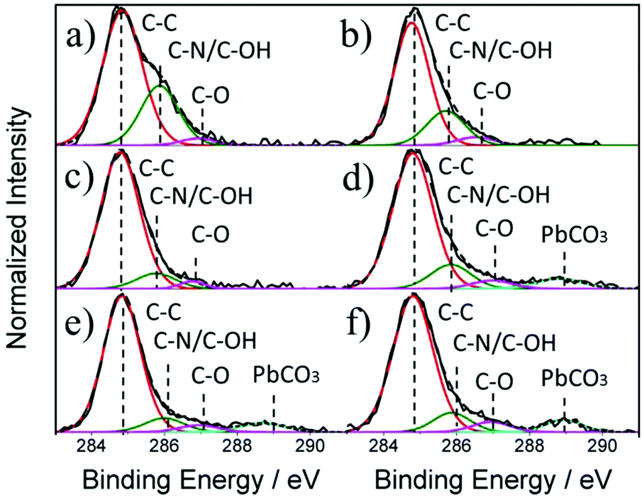 | ||
| Fig. 3 XPS core level spectra for C 1s where (a–f) represents decreasing MAPbI3 film thickness: (a) 4.99 μm, (b) 4.65 μm, (c) 2.67 μm, (d) 1.71 μm, (e) 1.37 μm and (f) 0.67 μm. | ||
Fig. 4a–f shows the XPS analysis of the O 1s region for MAPbI3 films of varying thickness. The O 1s spectra for our samples can be initially de-convoluted into two peaks found at 531.8 eV and 533.5 eV corresponding to O![[double bond, length as m-dash]](https://www.rsc.org/images/entities/char_e001.gif) C and OC–O respectively.28 These peaks are typical for most air exposed samples and are known as adventitious carbon, comprising of a variety of hydrocarbon species with both singly and doubly bound oxygen functionality. The appearance of a peak found at 530.4 eV (O′) is attributed mainly to weakly adsorbed OH− and O2− ions but has also been referenced as intercalated lattice O or PbO/Pb(OH)2 like states.27,28 MAPbI3 films are known to be significantly affected by surface oxidation where chemisorbed or dissociated oxygen species can diffuse and distort the MAPbI3 framework causing degradation. As the concentration of iodide ions reduces at the surface of our MAPbI3 films, the intercalated oxygen (O2−) can readily terminate Pb dangling bonds resulting in the formation of PbO/Pb(OH)2 like states. However, through XRD measurements it has been highlighted that Pb–O bonds in MAPbI2+x do not lead to the formation of secondary phases of PbO.29 The atomic mass percentages for our de-convoluted O 1s peaks was calculated from their integrated areas and plotted against MAPbI3 film thickness (Fig. 4g). The decrease in the O′ component coupled with the Increase in OC and OC–O components, highlight the ability for adsorbed oxygen species to more easily diffuse into thin MAPbI3 films.
C and OC–O respectively.28 These peaks are typical for most air exposed samples and are known as adventitious carbon, comprising of a variety of hydrocarbon species with both singly and doubly bound oxygen functionality. The appearance of a peak found at 530.4 eV (O′) is attributed mainly to weakly adsorbed OH− and O2− ions but has also been referenced as intercalated lattice O or PbO/Pb(OH)2 like states.27,28 MAPbI3 films are known to be significantly affected by surface oxidation where chemisorbed or dissociated oxygen species can diffuse and distort the MAPbI3 framework causing degradation. As the concentration of iodide ions reduces at the surface of our MAPbI3 films, the intercalated oxygen (O2−) can readily terminate Pb dangling bonds resulting in the formation of PbO/Pb(OH)2 like states. However, through XRD measurements it has been highlighted that Pb–O bonds in MAPbI2+x do not lead to the formation of secondary phases of PbO.29 The atomic mass percentages for our de-convoluted O 1s peaks was calculated from their integrated areas and plotted against MAPbI3 film thickness (Fig. 4g). The decrease in the O′ component coupled with the Increase in OC and OC–O components, highlight the ability for adsorbed oxygen species to more easily diffuse into thin MAPbI3 films.
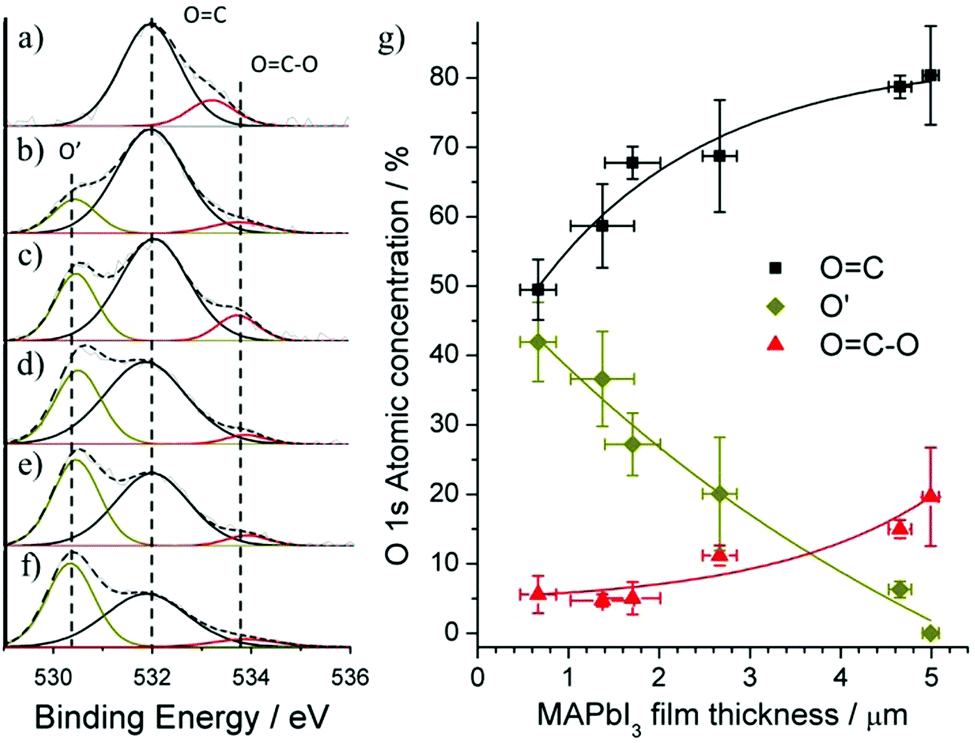 | ||
| Fig. 4 (a) X-ray photoelectron spectroscopy analysis of the O 1s region for decreasing MAPbI3 film thickness: (a) 4.99 μm, (b) 4.65 μm, (c) 2.67 μm, (d) 1.71 μm, (e) 1.37 μm and (f) 0.67 μm. (g) Summarized atomic mass concentration for each fitted component in the O 1s spectra. | ||
Binding energy of metallic Pb is typically found at lower energies in the region 136.3–136.9 eV,30 however during the perovskite formation there is a substantial alteration in Pb 4f core level due to the re-structuring of surface states to form Pb ions. The non-appearance of a metallic Pb state signifies strong charge transfer between Pb and I species to form donor–acceptor complexes. The Pb 6p valence state donates its excess unpaired electrons to the more electronegative iodide atoms where oxidation state Pb2+ is formed with iodide reducing to anion I2−.28,31 An additional iodide ion bonded with organic MA+ cation form weak van der Waals interaction with Pb–I framework to make up the PbI6 octahedral within the perovskite lattice. It follows that the Pb 4f spectra of the MAPbI3 films generally exhibit symmetrical peaks at 137.6 eV and 142.6 eV, corresponding to the spin orbit splitting of the Pb 4f7/2 and 4f5/2 components respectively that represent the Pb2+ cation in the MAPbI3 structure.32 The Pb 4f7/2 component of our MAPbI3 films with decreasing thickness is presented in Fig. 5a–f; the peak at 142.6 eV is not shown here but remains constant throughout the samples. For thicker film (Fig. 5a and b), the Pb 4f7/2 component is present with no other peak. As the film thickness is reduced, there is significant broadening in the accompanying Pb 4f spectra (Fig. 5c and d) that allows for the fitting of an additional peak around 138.4 eV attributed to the PbI2 component.33 The intensity of this PbI2 peak increases with decreasing MAPbI3 film thickness while the peak corresponding to Pb2+ state (137.6 eV) decreases (Fig. 5c–f). It is worth mentioning that a peak corresponding to PbO/Pb(OH)2 in the Pb 4f spectra has shown to also have a binding energy of around 138.4 eV34 and therefore may overlap with the PbI2 component. Reviewed literature highlights that PbO/Pb(OH)2 and PbI2 components can be found within binding energy ranges of 137.7–138.5 eV and 138.3–138.9 eV, respectively.35–37 However, weakly adsorbed oxygen species (O2−, OH−) highlighted previously in O 1s spectra (BE = 530.4 eV, Fig. 4a–f) indicate that only constrained/amorphous PbO/Pb(OH)2 like states may be formed due to the termination of Pb dangling bonds (iodide vacancies). Formation of crystalline PbO in the O 1s region is typically found at lower binding energies around 529 eV38 and therefore the loss of iodine ions resulting in PbI2 bonding arrangement is mainly responsible for the broadening observed in the Pb 4f spectra. Furthermore, the appearance of a third peak located at 139.1 eV is attributed to PbC2O4/PbCO3 bonds, consistent with Fig. 3, and has recently been shown to be an additional oxidation by-product of MAPbI3.27 The overall carbon concentration was observed to increase while the overall Pb concentration decreased by a comparable amount for thin MAPbI3 films (Fig. 2a): the C 1s/Pb 4f atomic ratio increased around 1.3 times with decreasing thickness. Since Pb cannot leave the film it can be concluded that surface polymerization produces a surface hydrocarbon layer, which may also limit the escape depth of Pb 4f photoelectrons. The fact that the carbonate (PbC2O4/PbCO3) component is more pronounced in the C 1s core level spectra compared with the Pb 4f core level is due to the photo ionization cross section of C 1s electrons being around 100 times lower than the Pb 4f electrons. Fig. 5g summarizes the concentrations derived from Pb 4f spectra, which highlights drastic changes taking place at the surface of the sprayed film. Thick films (>2 μm) resembling a typical MAPbI3 composition and thin films (<2 μm) exhibiting surface changes.
 | ||
| Fig. 5 (a) X-ray photoelectron spectroscopy analysis of the Pb 4f region for decreasing MAPbI3 film thickness: (a) 4.99 μm, (b) 4.65 μm, (c) 2.67 μm, (d) 1.71 μm, (e) 1.37 μm, (f) 0.67 μm and (g) summarized atomic concentration percentages for each fitted component in the Pb 4f spectra. | ||
XPS for core level I 3d exhibits two intense peaks for thicker films, corresponding to doublets 3d5/2 and 3d3/2 with the lower binding component located at 618.9 eV and is assigned to triiodide I3− (Fig. 6a–c).28 The shift to higher binding energy 619.1 eV (Fig. 6d–f) is associated with the loss of an iodide ion through MAI evaporation leaving the I2− anion from PbI2.33 Additional broadening of the I 3d spectra for thinner MAPbI3 films indicate the presence an additional peak at 620.2 eV that is credited to the oxidation of iodine at the surface which forms the I2+ cation and the iodite (IO2−) anion.28,30,33
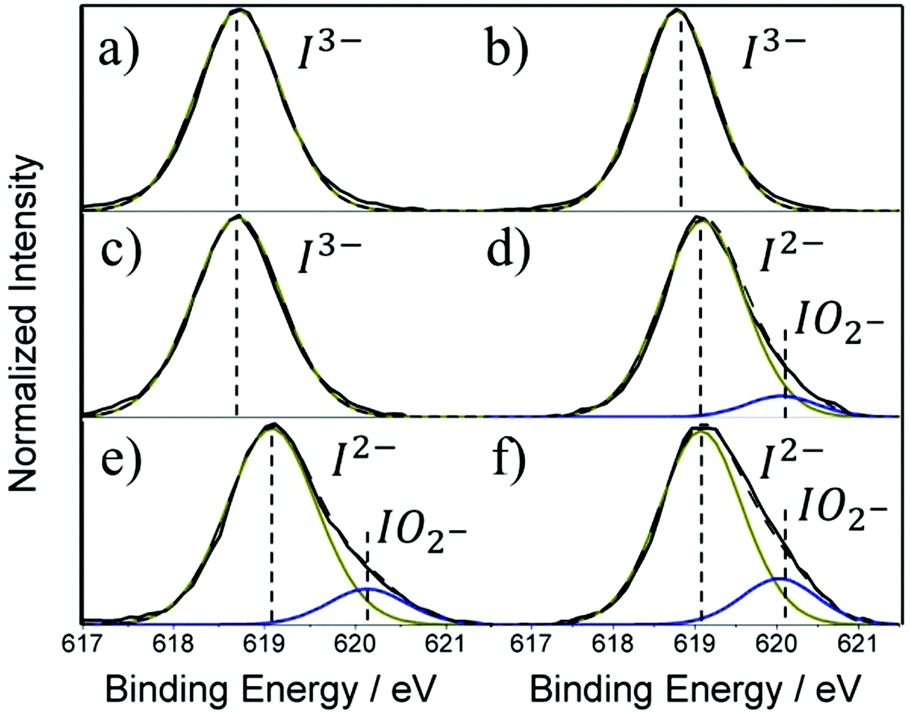 | ||
| Fig. 6 XPS core level spectra for I 3d where (a–f) represents decreasing MAPbI3 film thickness: (a) 4.99 μm, (b) 4.65 μm, (c) 2.67 μm, (d) 1.71 μm, (e) 1.37 μm and (f) 0.67 μm. | ||
Detailed XPS analysis of MAPbI3 films clearly indicates that spraying thinner MAPbI3 films allows for the formation of surface intermediate MAPbI2+x phases and finally surface PbI2 on the very top-layer (Fig. 7). The loss of iodine ions through the breakdown of the MAI component is closely linked with the increase in oxygen concentration at the films surface. For thinner MAPbI3 films, the concentration of adsorbed OH− and O2− ions increased relative to adventitious hydrocarbons (OC and OC–O) that are typically found on samples surface. These surface adsorbed species diffuse into the MAPbI3 and cause distortion of the perovskites framework where the MA cation is easily dissociated due to its weak interaction with PbI6 network. The destruction of the MAPbI3 lattice and specifically the organic core is also evident through the decrease in N 1s atomic concentration (Fig. 2a) even before NHx bonds are absent from the surface (see ESI†). The breakdown of the MAI component creates a number of iodine vacancies that can be easily terminated by intercalated oxygen species to create amorphous and constrained bonding arrangements such as PbO/Pb(OH)2, IO2− and PbCO3/PbC2O4. MAI can be further broken down into the volatile components CH3NH2 and HI and are evaporated leaving solid PbI2 at the surface.
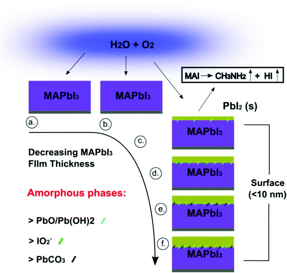 | ||
| Fig. 7 Schematic highlighting the changing surface chemistry for MAPbI3 films of decreasing thickness: (a) 4.99 μm, (b) 4.65 μm, (c) 2.67 μm, (d) 1.71 μm, (e) 1.37 μm and (f) 0.67. | ||
Surface morphology and grain analysis
SEM images of MAPbI3 films show the changing surface morphology with decreasing film thickness (Fig. 8). The grains transition from large micro sized cube like structures typical of MAPbI3 (Fig. 8a–c, thicker films) to de-agglomerated smaller distorted arrangements in thinner films (Fig. 8d–f) is evident, as the surface undergoes decomposition to MAPbI2+x/PbI2. Recent work involving density functional theory calculations have shown that defects, originating within the perovskites organic core, can be easily formed at room temperature.39 The generation of these defects therefore enhances interactions with atmospheric species where it is understood that the deprotonation of MA cation is the first degradation step. The creation of intrinsic volatile components (HI & CH3NH2) and succeeding desorption process within the MAPbI3 structure was shown to progressively erode the MAPbI3 lattice.40 Structural rearrangement of PbI6 octahedral due to the loss of I atoms to volatile components MAI and HI allows for PbI2 crystal seed to form simultaneously and gradually transform the MAPbI3 lattice into PbI2.41 The deagglomeration of large micro sized MAPbI3 grains (Fig. 8c–f) signifies this structural reorganization, occurring at the interface of MAPbI3 crystallites or at lattice defects within the grains. The subsequent increase in surface roughness accelerates the degradation process where micro sized PbI2 hexagonal structures being to form visibly at the surface (Fig. 8d and e). Quantitative grain analysis is performed for each film by selecting a small area with >15 grains (insets Fig. 8a–f) and using imageJ software. Plotting a histogram of grain size for each film (Fig. 8g) and a graph of grain size as a function of MAPbI3 thickness (Fig. 8h), it is observed that grain size decreases significantly as the surface decomposes from MAPbI3 to MAPbI2+x/PbI2. The size distribution of Fig. 8g has been fitted with Gaussian fits to produce mean size and standard deviation summarized in Fig. 8h. For sprayed films where the surface was experimentally determined to have I/Pb atomic mass close to 2:1, (Fig. 8d–f), the small distorted grains create a largely porous layer that presents a rough and non-uniform surface. This structural transformation and decreased grain sizes associated with PbI2 formation has been observed in multiple works, regardless of deposition technique.42–44
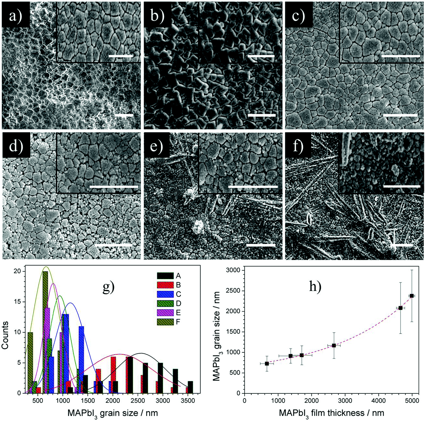 | ||
| Fig. 8 Surface scanning electron microscopy (SEM) images of MAPbI3 films at decreasing thickness: (a) 4.99 μm, (b) 4.65 μm, (c) 2.67 μm, (d) 1.71 μm, (e) 1.37 μm and (f) 0.67 μm. Insets show increased magnification images used for size analysis (all scale bars are set to 5 μm including insets). (g) Histogram of grain size analysis in the range 0–3750 nm and bin size 300 nm for films (a–f) with (h) plot of average grain size as a function of MAPbI3 film thickness where error bars for y-axis represent the SD of measured grain sizes for films (a–h). | ||
Electronic band structure
Low binding energy XPS scans (Fig. 9a) for MAPbI3 films with decreasing film thickness give insight into valence levels and can demonstrate more sensitivity to chemical interactions compared with core electrons. The XPS signal onset begins when highly kinetic/low binding photoelectrons from the outer most valence levels of MAPbI3 are bombarded by the X-ray source, escaping to vacuum level and to the electron detector. Valence band spectra exhibits a broad signal in the range 0–6 eV that can be de-convoluted into two peaks corresponding to I 5p non-bonding state with a right shoulder peak assigned to the anti-bonding hybrid state of Pb 6s and I 5p state.45,46 XPS analysis previously revealed that the total oxygen atomic concentration calculated from the integrated area under the core level O 1s increased for decreasing MAPbI3 film thickness (Fig. 2a). After peak fitting the spectra it was specified that an increase in OH− and O2− ions was the main cause (Fig. 4), indicating that thinner MAPbI3 films fabricated using one step spray method exhibited increased surface reactivity. The consequence of this increased interaction resulted in the enhanced surface decomposition of MAPbI3 to form MAPbI2+x through the evaporation of the MAI component. Once again it can be observed that reducing MAPbI3 film thickness increases the concentration of Pb 6s and I 5p state anti-bonding hybrid state relative to I 5p non-bonding state. Additionally, the decomposition of MAPbI3 to PbI2 also shifts the onset of XPS signal to higher binding energies. | ||
| Fig. 9 (a) X-ray photoelectron spectroscopy (XPS) valence region scans for decreasing MAPbI3 film thicknesses (4.99 μm, 4.65 μm, 2.67 μm, 1.71 μm, 1.37 μm, 0.67 μm) where Ef–VBM is valence band maximum energy relative to the Fermi energy (Ef). (b) Ef–VBM plotted as a function of MAPbI3 film thicknesses and corresponding I/Pb atomic mass ratio. (c) Absolute Fermi level measurements determined using Kelvin probe plotted as a function of MAPbI3 film thicknesses and corresponding I/Pb atomic mass ratio. | ||
Extrapolating the XPS signal through the x-axis enables calculation of the valence band maximum (VBM) energy relative to the Fermi level (Ef) for the MAPbI3 films. A number of studies have suggested that XPS-based measurements to determine VBM positions for air exposed MAPbI3 films are more consistent and reproducible when compared to measurements derived from ultraviolet photoelectron spectroscopy, since the latter provides information only to a depth of only 0.5–1 nm whereas the former provides information up to a 10 nm penetration depth.47–49 Therefore, XPS analysis minimizes effects of surface states due to contaminants on the electronic density of states profile since a larger penetration depth ensures measurement is more representative of bulk material properties. Plotting Ef–VBM for each of the MAPbI3 films shows decreasing energy separation from nearly 0.9 eV to 0.55 eV when going from a degraded 2:1 (yellow) to a stoichiometric 3:1 (blue) for I:Pb atomic ratio (Fig. 9b); for convenience we included here also the I:Pb atomic ratio from Fig. 2b. This implies that the Fermi level and the valence band are shifting away from each other as the film thickness is reduced and therefore moving from thicker weakly p-doped film to a more n-type thinner films. Experimental studies have highlighted the effects of Pb and I vacancies in MAPbI3 films and concluded that MAPbI3 films that are MAI deficient/PbI2 rich are typically n-doped whereas PbI2 deficient/MAI rich films are p-doped and is in good agreement with our experimental results.50,51
The VBM values determined using XPS measurements give values relative to the Fermi level which displays the energy separation and direction of Fermi movement successfully. However in order to establish absolute VBM positions relative to vacuum level the Fermi level of MAPbI3 films must be first determined. The Fermi level of MAPbI3 films has been measured using a Kelvin probe (Fig. 9c) that measures the contact potential difference of material relative to a known work function reference, in this case gold (−5.1 eV). Plotting MAPbI3 Fermi level against film thickness shows that for thicker MAPbI3 (I:Pb = 3:1) the Fermi level is −5.05 eV and is agreeable with literature;52 also here in this case we have included the I:Pb atomic ratio from Fig. 2b. Reducing the MAPbI3 film thickness decreases the I:Pb ratio to around 2.5:1 meaning that a high number of MA and I vacancies are present at the film surface with consequent reduction (in absolute values) of the Fermi level to −5 eV. This confirms the effect of MA and I deficiencies, which promote n-doping behaviour in MAPbI3 films. Decreasing film thickness further where the I:Pb atomic mass ratio is <2.2:1 causes a gradual decrease (in absolute value) in the Fermi level to around −4.8 eV. The initial slow shift of the Fermi level can be attributed to the loss of MA and I concentration and associated vacancies, however it is not until after PbI2 begins to form on our film surface (I:Pb atomic ratio <2.2) that the Fermi level noticeably shifts. It should be emphasized that depending on the thickness of the PbI2 surface layer there may be some Fermi level pinning from the underlying MAPbI3/PbI2 interface which can explain the gradual increase in Fermi level as the thickness of PbI2 layer increases. As PbI2 crystallizes and grows the influence of the underlying MAPbI3 electronic states become less significant until the value of the Fermi level reduces (in absolute values) to that of pure PbI2.
Photovoltaic performance of sprayed MAPbI3 films
In order to understand the effect of the surface chemistry for spray deposited MAPbI3 films, typical current density–voltage (JV) characteristics were measured under AM 1.5 illumination in air. An increase in current density (JSC), open circuit voltage (VOC) and overall power conversion efficiency (PCE) was observed for progressively thinner MAPbI3 absorbers. The PCE increases exponentially from 0.83% to 5.23% with decreasing film thickness due to the matching of the MAPbI3 carrier diffusion length (Fig. 10b). Examining individual parameters of our MAPbI3 devices (VOC, FF, JSC) we find that the main reason for increased PCE is the significant increase in JSC from 4.9 mA cm−2 to 22.3 mA cm−2 with the VOC also increasing from 0.52 V to 0.73 V (Fig. 10c). | ||
| Fig. 10 (a) Illuminated current density–voltage characteristics of our devices with decreasing MAPbI3 film thickness, (A–F) represents MAPbI3 film thickness of (a) 4.99 μm, (b) 4.65 μm, (c) 2.67 μm, (d) 1.71 μm, (e) 1.37 μm and (f) 0.67 μm, (b) power conversion efficiency vs. decreasing MAPbI3 film thickness and (c) individual device parameters VOC, FF and JSCvs. decreasing MAPbI3 film thickness. Dotted lines are the result of exponential fitting using Origin software. | ||
Depending on processing technique, diffusion lengths in the range 200–500 nm have been observed for MAPbI3 films which closely match typical film thicknesses seen in high efficiency MAPbI3 devices.53 However for devices that have used spray coating, optimal thin films cannot be produced yet and thicker films are generally obtained. Also in our case, reducing the film thickness further to <500 nm using spray technique proved difficult and produced extremely porous films exhibiting small rod like structures assumed to be PbI2 (ESI†). The incorporation of these low thickness films in PV devices resulted in shunting behavior that is attributed to the non-homogeneity of the sprayed film. The increased degradation for thin sprayed films (<500 nm) is in good agreement with trend of the surface chemical changes for decreasing MAPbI3 films (Fig. 2, 4 and 5). Our thinnest sprayed MAPbI3 film (670 nm thickness) gave the greatest PCE of 5.23% due to the optimization of absorber thickness close to carrier diffusion lengths.
The consistently low FF of around 0.33 could be in principle improved considerably by including a hole transport material (HTM), where incorporation of Spiro-OMeTAD in perovskite based devices has shown efficiencies increase beyond 20%.2,3 However, since the spray deposition method used in this technique is fairly novel and to better assess the band alignment and energy band level changes with respect to a known stable metal (i.e. Au), it was decided to first understand the surface chemistry of as deposited MAPbI3 films before inclusion of sequential layers. As the inclusion of an HTM such as spiro-OMeTAD has been widely reported to improve device efficiency, we expect this to happen also for these sprayed MAPbI3 films. In any case, as our work clearly point out, spray deposition still has to overcome degradation challenges before optimal thin perovskite films can be produced to be competitive with devices produced by other methods. According to the equivalent circuit (ESI†), the JV characteristic can be described as
 | (1) |
 | (2) |
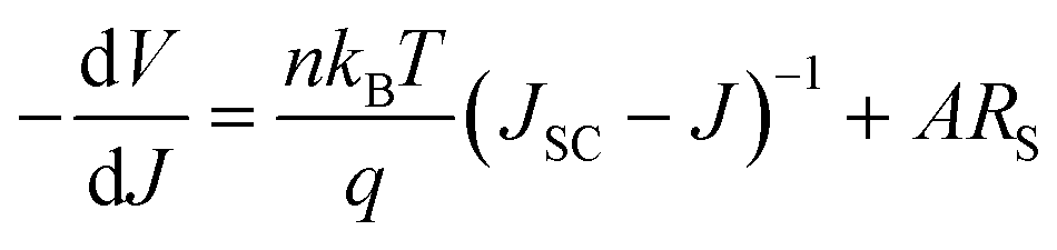
Fig. 11a shows the plots of −dV/dJ vs. (JSC − J)−1 and the linear fitting curves according to eqn (2). Our cells show a linear relationship between −dV/dJ and (JSC − J)−1 in the region approaching the VOC. The area normalized series resistance (ARS) of the cells can be deduced from the intercept of the linear fitting results in the region approaching (JSC − J)−1 = 0.55 We observe ARS of our devices reducing from 33.4 Ω cm2 to 7.2 Ω cm2 with decreasing MAPbI3 film thickness and as a consequence we observe a large increase in the devices JSC. Additionally, the JV curves can be used to determine the voltage dependant ideality factor (n) of devices for values from 0 V up to the corresponding VOC (Fig. 11b). When plotting the natural log of the current density against the voltage, the slope q/nkBT gives a value for n.56 In a heterojunction solar cell, values of n can give an insight into the quality of a junction and the carrier recombination mechanisms. The ideality factor is typically in the range 1 < n < 2, for a “well-behaved” heterojunction.56 When the junction is dominated by the carrier diffusion in the neutral region, n is at low values of 1. On the other hand, when carrier recombination in the depleted space charge region dominates the current, n is moving away from unity. In most cases, both carrier diffusion and recombination take place simultaneously.55,56
 | ||
| Fig. 11 (a) Plot of −dV/dJ vs. (JSC − J)−1 for devices with decreasing MAPbI3 film thickness and extrapolated linear fit near (JSC − J)−1 = 0 (b) voltage dependant ideality factor of the devices with abnormally low and high values emphasized. (A–F) Represents MAPbI3 film thickness of (a) 4.99 μm, (b) 4.65 μm, (c) 2.67 μm, (d) 1.71 μm, (e) 1.37 μm and (f) 0.67 μm. | ||
High values for ideality factor can also be caused by various other effects such as interface states, tunnelling processes and non-uniform distribution of interfacial charges.57–59 More specifically interface dipoles due to interface doping as well as fabrication induced defects play an important role in the performance and reliability of metal/semiconductor structures.60 Looking at Fig. 11b, we see that n increases with voltage approaching VOC for each device. For the two devices with the greatest MAPbI3 film thickness (black squares/red circles), the ideality factor is between values of 1 to 2 in the range 0 V to the device VOC. As we reduce our MAPbI3 film thickness within our solar cell, we see that the value of n beings to exceed 2 in the region approaching each devices specific VOC and falls below 1 at voltages <0.3 V. Ideality factor moving away from unity approaching VOC has previously been highlighted for MAPbI3 HTM free solar cells56,61 and suggests that the current is mainly controlled by the recombination in the space charge region of the TiO2 and MAPbI3 layers. However, ideality factors above 2 have been previously shown to be a clear indication of trap assisted tunnelling or field enhanced recombination through isolated point defects.62,63
Nonetheless, the highlighted areas suggest poor Schottky contact effect in our devices for thin MAPbI3 films. The fact that decreasing MAPbI3 film thickness produces smaller grain boundaries as highlighted earlier, may explain why the ideality factor drops below unity. The smaller grains/increased grain boundaries clearly increase the potential for recombination through surface states before carriers can be successfully collected at the back contact. Light soaking effects over a period of 0–6 min, including effect on individual parameters were collected (ESI†). Comparing light soaking effects on PCE for 3 devices that represent the maximum, minimum and intermediate MAPbI3 absorber thickness (Fig. 12), a distinct trend can be observed. Thick MAPbI3 film exhibits lowest PCE (<1%) most likely due to the thickness being larger than the carrier diffusion length; however with continued light soaking over a time period of 6 min the PCE significantly increases to more than 3%. For MAPbI3 film with intermediate thickness (i.e. 2.67 μm) the beneficial light soaking effect is diminished and the PCE drops slightly from 2.9% to around 2% over the same time period. Finally for the thinner MAPbI3 film (0.67 μm), the PCE at 0 min illumination is more than 5%. However increasing the time under illumination induces notable negative impact with the PCE decreasing from >5% to less than 2%.
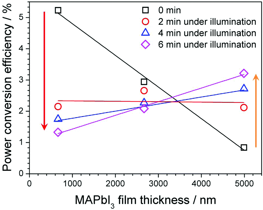 | ||
| Fig. 12 Power conversion efficiency of devices with maximum, intermediate and minimum MAPbI3 film thickness of 5 μm, 2.6 μm and 0.6 μm respectively, at 0 min, 2 min, 4 min and 6 min under illumination. | ||
Discussion
PV performance of our thicker MAPbI3 devices (∼5 μm) showed a relatively low JSC measured at 0 minutes (Fig. 10c) before increasing considerably after 6 min light soaking (4.9 mA cm−2 to 14 mA cm−2, see ESI†), corresponding to the behaviour of the PCE (Fig. 12). This light soaking phenomena is generally observed for perovskite devices where the PCE is typically presented after stabilization at the maximum power point which takes place in a short time scale (0–3 min).64,65 The stabilization period is understood to be caused by the filling of shallow charge trap sites by photo generated electrons or migrating ions, shifting the quasi-Fermi-level for electrons and therefore VOC increases (Fig. 13, 0 min). The reduction in trap site density also increases JSC accordingly due to the reduction in non-radiative pathways available.64 Recently photo-induced brightening of MAPbI3 photoluminescence was demonstrated and attributed to an order of magnitude reduction in trap state density due to migration of iodide ions.7 Due to the high number of oxygen vacancies (VO) that are expected in TiO2, many of the photo excited carriers (e−) may become trapped at the interface which can create electric fields and encourage iodide ion (I−) migration.66 The mobile iodide ions migrate away from the incident illumination into the MAPbI3 film and fill iodide vacancies (VI) that translate as shallow states below (above) the CBM (VBM) (Fig. 13, 2–4 min).67 The annihilation of these defects under increased light soaking would result in the shifting of quasi-Fermi level and the reduction of non-radiative recombination pathways, largely increasing open circuit voltage and photo carrier collection (Fig. 13, 6 min). | ||
| Fig. 13 Schematic showing the potential photo induced cleaning due to halide distribution that can explain light soaking stabilization period experienced in MAPbI3 films under illumination. | ||
Depending on processing technique, diffusion lengths in the range 200–500 nm have been observed for MAPbI3 films which closely match typical film thicknesses seen in high efficiency MAPbI3 devices.53 Therefore, in order to optimize the photo generated current from spray deposited MAPbI3 films presented in this work, absorber thickness was reduced to around the same magnitude of carrier diffusion lengths. Decreasing the MAPbI3 film thickness increased overall carrier collection as a substantial increase in PV performance at 0 minutes is observed for devices (Fig. 10b and c). It is known that MAPbI3 films are susceptible to chemical decomposition that originates from chemisorbed or dissociated oxygen species and XPS analysis has highlighted that this modification is accelerated at the surface of thin spray-coated films with the increase of OH−/O2− surface species. Energy bands are displayed for MAPbI3 films of decreasing thickness and changing surface chemistry (Fig. 14). Figure labels (a–f) correspond to varying film thickness of 4.99 μm, 4.65 μm, 2.67 μm, 1.71 μm, 1.37 μm and 0.67 μm, respectively. XPS, Kelvin probe and UV-Vis measurements correlate well to show that reduced PbI2 on the surface creates a type-1 hetero-junction with the underlying MAPbI3. Energy levels presented here are non-equilibrated however it is evident that a significant potential barrier would exist for hole extraction at the back electrode (Fig. 14c–f). This is in agreement with a previous report that claimed a type-1 alignment of PbI2 with MAPbI3 (VB and CB located at −5.75 and −3.45 eV) and a potential barrier of 30–50 mV.68
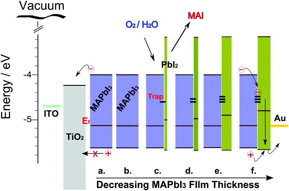 | ||
| Fig. 14 Energy band structures for our device architectures showing changes in surface chemistry and how subsequent electron transfer process may be affected for decreasing MAPbI3 film thickness: (a) 4.99 μm, (b) 4.65 μm, (c) 2.67 μm, (d) 1.71 μm, (e) 1.37 μm and (f) 0.67 μm. Energy level are non-equilibrated. The absolute values of the band edges and Fermi levels for the MAPI3 and PbI2 layer are taken from our experimental measurements (Fig. 9b and c) and bandgap values from literature. | ||
From theoretical simulations, the majority of defects in MAPbI3 have low formation energies and create shallow levels within the bandgap,67 which are unlikely to influence our Fermi level measurements. However these theoretical simulations were carried out on the assumption of pure perovskite phases. It is important to note however that the formation of different phases at the surface of MAPbI3 films, such as those highlighted in this study (i.e. PbI2, Fig. 14c–f), can result in low energy/deep defect states and potentially influence the Fermi levels determined experimentally in this work.69 Moreover, these defect states can provide mid gap levels at which carriers can recombine thus suppressing carrier collection at the back electrode.
Counter to the beneficial light soaking effects observed for MAPbI3 devices in this work (for thicker films, Fig. 12 and 14a, b) and also in the literature, we notice a contradictory trend for spray-coated thin films (Fig. 12 and 14c–f) that we attribute directly to the changing surface chemistry and subsequent defect states at the back electrode. A MAPbI2+x film (I/Pb atomic ratio = 2.5:1) whose surface (<10 nm) has been degraded from the initial stoichiometric crystal showed a decrease in JSC over a period of 0–6 min under illumination (15.15 mA cm−2 to 13.86 mA cm−2). This decrease in PV performance correlates directly with the changing surface chemistry where an increase in adsorbed oxygen species has resulted in the decomposition of MAPbI3 structure. This instability under light soaking is exacerbated for a number of thinner films that show an initially high PCE before JSC and VOC significantly decrease over a period of 6 min. More specifically, a device incorporating a film with measured thicknesses of 0.67 μm showed the greatest PCE of 5.23% which decreased to 1.3% after 6 minutes continuous light soaking (Fig. 12). The quantified surface composition determined from XPS measurements showed an overall increase in O 1s atomic mass that was explicitly due to intercalated OH− and O2− species originating from adsorbed atmospheric species. The different morphologies are the determining factor for the surface chemistry where the increased surface to volume ratio that exist for thinner MAPbI3 sprayed films imposes a large degree of surface stress and strain which limits the chemical stability under ambient conditions. In turn, the formation of different grain size distributions is a consequence of the aerosol droplet size and velocity distributions which affect how the droplets coalescence and subsequently evaporate on the dynamic growing surface. These factors are in turn influenced by input parameters (solution composition, gas flow and spraying conditions) and the evolving topography and thermal properties of the surface. Present results show that, for thinner MAPbI3 films, a morphology with larger surface area increases the surface interactions with ambient atmospheric species, which are most likely responsible for a higher density of surface defects. These defects originate during the spray process annealing stage which allows the continuous adsorption of atmospheric species. The increased adsorption and interaction of OH−/O2− species leads to distortion of the perovskite lattice where the MA cation is originally dissociated due to weak van der Waals bonds with PbI6 network. Recent work has highlighted that water vapour reactions, which lead to the formation of MAPbI3–H2O and MAPbI3–2H2O hydrate phases and consequential hysteresis in solar devices, are reversible.70 Water molecules form hydrogen bonds with surface halide, however no proton transfer happens unlike the situation with adsorbed OH radicals and OH− species, where accelerated perovskite decomposition has been shown to occur.70 The resulting hydrogen/proton extraction from the surface MA cations forming surface CH3NH2 is suggested as the initial step in the degradation process with further breakdown producing NH2 and HI components. The former can be easily evaporated whereas the latter can react with O2 to form I2 and H2O or decompose into I2 and H2.71 The same degradation path is evident here due to the experimentally observed decrease in both N 1s and I 3d atomic mass concentrations in addition to the Pb 4f core level shifting to a higher binding energies associated with the loss of iodide ions.
The interplay between oxygen and MAPbI3 films has been well documented where films have exhibited poor morphologies and incomplete surface coverage under high oxygen concentrations. The distorted grain structure among inferior crystallinity observed in MAPbI3 films in this study is clear evidence of oxygen detrimental effect on chemical stability. Moreover, electron–hole recombination lifetimes have been shown to dramatically shorten with increasing oxygen concentration along with substantial quenching of photoluminescence,29,72 suggesting that intercalated oxygen species may act as deep trap centres for photo excited carriers. The high ideality factors demonstrated for thin MAPbI3 films (Fig. 11b) indicated poor Schottky contact effect and trap assisted recombination at the back electrode. The fact that devices, where surface decomposition (<10 nm) has occurred (MAPbI3 to MAPbI2+x/PbI2), exhibit good PV performance initially at 0 minutes before the photocurrent and open circuit voltage are degraded under continued light soaking (0–6 minute) suggests that trap sites become filled before consequently forming macroscopic charged regions, increasing the potential barrier between bulk MAPbI3 and surface PbI2.
Conclusion
A rapid one step spray technique that possesses the potential for large scale manufacture has been implemented to fabricate MAPbI3 absorber films with varying thickness and corresponding power conversion efficiencies from 0.83% to 5.22%. Investigation into the stability of devices under constant illumination showed conflicting behaviour with low efficiency (thick) MAPbI3 films and high efficiency (thin) MAPbI3 films, where the former displayed large increases in overall performance compared to rapid reductions experienced in the latter. It was experimentally concluded that the surface modification was directly related to instability of device performance under light soaking conditions. Determination of the Fermi level showed a net upward shift near the surface when transitioning from pristine MAPbI3 to MAPbI2+x/PbI2. The measured energy separation Ef–VBM showed a comparable increase resulting in a potential barrier at the back contact that would significantly imped hole extraction. It was predicted however that the combined effect of intercalated OH−/O2− species, constrained amorphous states and dangling bonds due to I vacancies created a high density of shallow and deep level trap states that assisted in the non-radiative recombination of carriers. The spray deposition process demonstrated in this work can accelerate surface modification for thin films which is detrimental to PV performance under light soaking. Overall, this study suggests that deposition by spray method may enhance interactions of the solution being sprayed with atmosphere oxygen. The deployment of spray technologies will therefore need to take into account and reduce such detrimental impact. Future work will involve improvement of the one-step spray technique for MAPbI3 thin film deposition for use in high efficiency solar cells among other applications.Acknowledgements
This work has been partially funded by the Leverhulme Trust (IN-2012-136) and the EPSRC (EP/K022237/1 and EP/M024938/1). CR would like to acknowledge the support for the Northern Ireland Department for Employment and Learning (DEL). This work was also partially supported by a NEDO Project (Japan).References
- R. Fan, Y. Huang, L. Wang, L. Li, G. Zheng and H. Zhou, The Progress of Interface Design in Perovskite-Based Solar Cells, Adv. Energy Mater., 2016, 1600460 CrossRef.
- J. Burschka, N. Pellet, S.-J. Moon, R. Humphry-Baker, P. Gao, M. K. Nazeeruddin and M. Grätzel, Sequential Deposition as a Route to High-Performance Perovskite-Sensitized Solar Cells, Nature, 2013, 499(7458), 316–320 CrossRef CAS PubMed.
- M. Liu, M. B. Johnston and H. J. Snaith, Efficient Planar Heterojunction Perovskite Solar Cells by Vapour Deposition_web, Nature, 2013, 501(7467), 395–398 CrossRef CAS PubMed.
- S. A. Kulkarni, T. Baikie, P. P. Boix, N. Yantara, N. Mathews and S. Mhaisalkar, Band-Gap Tuning of Lead Halide Perovskites Using a Sequential Deposition Process, J. Mater. Chem. A, 2014, 2, 9221 CAS.
- C. Liu, J. Fan, X. Zhang, Y. Shen, L. Yang and Y. Mai, Hysteretic Behavior upon Light Soaking in Perovskite Solar Cells Prepared via Modified Vapor-Assisted Solution Process, ACS Appl. Mater. Interfaces, 2015, 7(17), 9066–9071 CAS.
- Y. Deng, Z. Xiao and J. Huang, Light-Induced Self-Poling Effect on Organometal Trihalide Perovskite Solar Cells for Increased Device Efficiency and Stability, Adv. Energy Mater., 2015, 5(20), 1–6 Search PubMed.
- D. W. deQuilettes, W. Zhang, V. M. Burlakov, D. J. Graham, T. Leijtens, A. Osherov, V. Bulović, H. J. Snaith, D. S. Ginger and S. D. Stranks, Photo-Induced Halide Redistribution in Organic–inorganic Perovskite Films, Nat. Commun., 2016, 7, 11683 CrossRef CAS PubMed.
- S. Meloni, T. Moehl, W. Tress, M. Franckevičius, M. Saliba, Y. H. Lee, P. Gao, M. K. Nazeeruddin, S. M. Zakeeruddin, U. Rothlisberger and M. Graetzel, Ionic Polarization-Induced Current–voltage Hysteresis in CH3NH3PbX3 Perovskite Solar Cells, Nat. Commun., 2016, 7, 10334 CrossRef CAS PubMed.
- B. Wu, K. Fu, N. Yantara, G. Xing, S. Sun, T. C. Sum and N. Mathews, Charge Accumulation and Hysteresis in Perovskite-Based Solar Cells: An Electro-Optical Analysis, Adv. Energy Mater., 2015, 5(19), 1–8 Search PubMed.
- A. A. Bakulin, O. Selig, H. J. Bakker, Y. L. A. Rezus, C. Müller, T. Glaser, R. Lovrincic, Z. Sun, Z. Chen, A. Walsh, J. M. Frost and T. L. C. Jansen, Real-Time Observation of Organic Cation Reorientation in Methylammonium Lead Iodide Perovskites, J. Phys. Chem. Lett., 2015, 6(18), 3663–3669 CrossRef CAS PubMed.
- J. H. Heo, D. H. Song, H. J. Han, S. Y. Kim, J. H. Kim, D. Kim, H. W. Shin, T. K. Ahn, C. Wolf, T.-W. Lee and S. H. Im, Planar CH3NH3PbI3 Perovskite Solar Cells with Constant 17.2% Average Power Conversion Efficiency Irrespective of the Scan Rate, Adv. Mater., 2015, 27(22), 3424–3430 CrossRef CAS PubMed.
- F. Polarization, N. H. Pbi, H. Kim, S. K. Kim, B. J. Kim, K. Shin, M. K. Gupta, H. S. Jung, S. Kim and N. Park, Ferroelectric Polarization in CH3NH3PbI3 Perovskite, J. Phys. Chem. Lett., 2015, 6, 1729–1735 CrossRef PubMed.
- J. Haruyama, K. Sodeyama, L. Han and Y. Tateyama, First-Principles Study of Ion Diffusion in Perovskite Solar Cell Sensitizers, J. Am. Chem. Soc., 2015, 137(32), 10048–10051 CrossRef CAS PubMed.
- O. Malinkiewicz, A. Yella, Y. H. Lee, G. M. M. Espallargas, M. Graetzel, M. K. Nazeeruddin and H. J. Bolink, Perovskite Solar Cells Employing Organic Charge-Transport Layers, Nat. Photonics, 2014, 8(2), 128–132 CrossRef CAS.
- C.-C. Chen, Z. Hong, G. Li, Q. Chen, H. Zhou and Y. Yang, One-Step, Low-Temperature Deposited Perovskite Solar Cell Utilizing Small Molecule Additive, J. Photonics Energy, 2015, 5(1), 057405 CrossRef.
- H.-L. Hsu, C.-P. Chen, J.-Y. Chang, Y.-Y. Yu and Y.-K. Shen, Two-Step Thermal Annealing Improves the Morphology of Spin-Coated Films for Highly Efficient Perovskite Hybrid Photovoltaics, Nanoscale, 2014, 6(17), 10281–10288 RSC.
- Q. Chen, H. Zhou, Z. Hong, S. Luo, H.-S. Duan, H.-H. Wang, Y. Liu, G. Li and Y. Yang, Planar Heterojunction Perovskite Solar Cells via Vapor-Assisted Solution Process, J. Am. Chem. Soc., 2014, 136(2), 622–625 CrossRef CAS PubMed.
- Z. Song, S. C. Watthage, A. B. Phillips and M. J. Heben, Pathways toward High-Performance Perovskite Solar Cells: Review of Recent Advances in Organo-Metal Halide Perovskites for Photovoltaic Applications, J. Photonics Energy, 2016, 6(2), 22001 CrossRef.
- W. Hwang, G. Xin, M. Cho, S. M. Cho and H. Chae, Electrospray Deposition of Polymer Thin Films for Organic Light-Emitting Diodes, Nanoscale Res. Lett., 2012, 7(1), 52 CrossRef PubMed.
- S. F. Tedde, J. Kern, T. Sterzl, J. Fürst, P. Lugli and O. Hayden, Fully Spray Coated Organic Photodiodes, Nano Lett., 2009, 9(3), 980–983 CrossRef CAS PubMed.
- M. Shao, S. Das, K. Xiao, J. Chen, J. K. Keum, I. N. Ivanov, G. Gu, W. Durant, D. Li and D. B. Geohegan, High-Performance Organic Field-Effect Transistors with Dielectric and Active Layers Printed Sequentially by Ultrasonic Spraying, J. Mater. Chem. C, 2013, 1(28), 4384 RSC.
- C. Girotto, D. Moia, B. P. Rand and P. Heremans, High-Performance Organic Solar Cells with Spray-Coated Hole-Transport and Active Layers, Adv. Funct. Mater., 2011, 21(1), 64–72 CrossRef CAS.
- R. C. Tenent, T. M. Barnes, J. D. Bergeson, A. J. Ferguson, B. To, L. M. Gedvilas, M. J. Heben and J. L. Blackburn, UItrasmooth, Large-Area, High-Uniformity, Conductive Transparent Single-Walled-Carbon-Nanotube Films for Photovoltaics Produced by Ultrasonic Spraying, Adv. Mater., 2009, 21(31), 3210–3216 CrossRef CAS.
- G. Grancini, V. D’Innocenzo, E. R. Dohner, N. Martino, A. R. Srimath Kandada, E. Mosconi, F. De Angelis, H. I. Karunadasa, E. T. Hoke and A. Petrozza, CH3NH3PbI3 Perovskite Single Crystals: Surface Photophysics and Their Interaction with the Environment, Chem. Sci., 2015, 6(12), 7305–7310 RSC.
- A. L. Abdelhady, M. I. Saidaminov, B. Murali, V. Adinolfi, O. Voznyy, K. Katsiev, E. Alarousu, R. Comin, I. Dursun, L. Sinatra, E. H. Sargent, O. F. Mohammed and O. M. Bakr, Heterovalent Dopant Incorporation for Bandgap and Type Engineering of Perovskite Crystals, J. Phys. Chem. Lett., 2016, 7(2), 295–301 CrossRef CAS PubMed.
- S. Barman and M. Sadhukhan, Facile Bulk Production of Highly Blue Fluorescent Graphitic Carbon Nitride Quantum Dots and Their Application as Highly Selective and Sensitive Sensors for the Detection of Mercuric and Iodide Ions in Aqueous Media, J. Mater. Chem., 2012, 22(41), 21832 RSC.
- W. Huang, J. S. Manser, P. V. Kamat and S. Ptasinska, Evolution of Chemical Composition, Morphology, and Photovoltaic Efficiency of CH3NH3PbI3 Perovskite under Ambient Conditions, Chem. Mater., 2016, 28(1), 303–311 CrossRef CAS.
- G. Rajendra Kumar, A. Dennyson Savariraj, S. N. Karthick, S. Selvam, B. Balamuralitharan, H.-J. Kim, K. K. Viswanathan, M. Vijaykumar and K. Prabakar, Phase Transition Kinetics and Surface Binding States of Methylammonium Lead Iodide Perovskite, Phys. Chem. Chem. Phys., 2016, 18(10), 7284–7292 RSC.
- W. Kong, A. Rahimi-Iman, G. Bi, X. Dai and H. Wu, Oxygen Intercalation Induced by Photocatalysis on the Surface of Hybrid Lead Halide Perovskites, J. Phys. Chem. C, 2016, 120(14), 7606–7611 CAS.
- T.-W. Ng, C.-Y. Chan, M.-F. Lo, Z. Q. Guan and C.-S. Lee, Formation Chemistry of Perovskites with Mixed Iodide/chloride Content and the Implications on Charge Transport Properties, J. Mater. Chem. A, 2015, 3(17), 9081–9085 CAS.
- J.-H. Lee, N. C. Bristowe, P. D. Bristowe and A. K. Cheetham, Role of Hydrogen-Bonding and Its Interplay with Octahedral Tilting in CH3NH3PbI3, Chem. Commun., 2015, 51(29), 6434–6437 RSC.
- H. Xie, X. Liu, L. Lyu, D. Niu, Q. Wang, J. Huang and Y. Gao, Effects of Precursor Ratios and Annealing on Electronic Structure and Surface Composition of CH3NH3PbI3 Perovskite Films, J. Phys. Chem. C, 2016, 120(1), 215–220 CAS.
- J. Zhang, T. Song, Z. Zhang, K. Ding, F. Huang and B. Sun, Layered Ultrathin PbI 2 Single Crystals for High Sensitivity Flexible Photodetectors, J. Mater. Chem. C, 2015, 3(17), 4402–4406 RSC.
- D. Chen, W. Shen, S. Wu, C. Chen, X. Luo and L. Guo, Ion Exchange Induced Removal of Pb(II) by MOF-Derived Magnetic Inorganic Sorbents, Nanoscale, 2016, 8(13), 7172–7179 RSC.
- J. M. Luther, M. Law, Q. Song, C. L. Perkins, M. C. Beard and A. J. Nozik, Structural, Optical, and Electrical Properties of Self-Assembled Films of PbSe Nanocrystals Treated with 1,2-Ethanedithiol, ACS Nano, 2008, 2(2), 271–280 CrossRef CAS PubMed.
- C. H. Jo, J. H. Kim, J. Kim, J. Kim, M. S. Oh, M. S. Kang, M.-G. Kim, Y.-H. Kim, B.-K. Ju and S. K. Park, Low-Temperature Annealed PbS Quantum Dot Films for Scalable and Flexible Ambipolar Thin-Film-Transistors and Circuits, J. Mater. Chem. C, 2014, 2(48), 10305–10311 RSC.
- Z. Zheng, A. Liu, S. Wang, Y. Wang, Z. Li, W. M. Lau and L. Zhang, In Situ Growth of Epitaxial Lead Iodide Films Composed of Hexagonal Single Crystals, J. Mater. Chem., 2005, 15(42), 4555 RSC.
- S. Rondon, Core Level and Valence Band Spectra of PbO by XPS, Surf. Sci. Spectra, 1998, 5(2), 97 CrossRef CAS.
- I. Deretzis, A. Alberti, G. Pellegrino, E. Smecca, F. Giannazzo, N. Sakai, T. Miyasaka and A. La Magna, Atomistic Origins of CH3NH3PbI3 Degradation to PbI2 in Vacuum, Appl. Phys. Lett., 2015, 106(13), 131904 CrossRef.
- J. M. Frost, K. T. Butler, F. Brivio, C. H. Hendon, M. van Schilfgaarde and A. Walsh, Atomistic Origins of High-Performance in Hybrid Halide Perovskite Solar Cells, Nano Lett., 2014, 14(5), 2584–2590 CrossRef CAS PubMed.
- A. Alberti, I. Deretzis, G. Pellegrino, C. Bongiorno, E. Smecca, G. Mannino, F. Giannazzo, G. G. Condorelli, N. Sakai, T. Miyasaka, C. Spinella and A. La Magna, Similar Structural Dynamics for the Degradation of CH3NH3PbI3 in Air and in Vacuum, ChemPhysChem, 2015, 16(14), 3064–3071 CrossRef CAS PubMed.
- X. Tong, F. Lin, J. Wu and Z. M. Wang, High Performance Perovskite Solar Cells, Adv. Sci., 2016, 3(5), 1500201 CrossRef PubMed.
- B. Philippe, B.-W. Park, R. Lindblad, J. Oscarsson, S. Ahmadi, E. M. J. Johansson and H. Rensmo, Chemical and Electronic Structure Characterization of Lead Halide Perovskites and Stability Behavior under Different Exposures—A Photoelectron Spectroscopy Investigation, Chem. Mater., 2015, 27(5), 1720–1731 CrossRef CAS.
- T.-B. Song, Q. Chen, H. Zhou, C. Jiang, H.-H. Wang, Y. (Michael) Yang, Y. Liu, J. You and Y. Yang, Perovskite Solar Cells: Film Formation and Properties, J. Mater. Chem. A, 2015, 3(17), 9032–9050 CAS.
- Y. Yuan, R. Xu, H.-T. Xu, F. Hong, F. Xu and L.-J. Wang, Nature of the Band Gap of Halide Perovskites ABX 3 (A = CH3NH3, Cs; B = Sn, Pb; X = Cl, Br, I): First-Principles Calculations, Chin. Phys. B, 2015, 24(11), 116302 CrossRef.
- H. Xu, Y. Wu, J. Cui, C. Ni, F. Xu, J. Cai, F. Hong, Z. Fang, W. Wang, J. Zhu, L. Wang, R. Xu and F. Xu, Formation and Evolution of the Unexpected PbI2 Phase at the Interface during the Growth of Evaporated Perovskite Films, Phys. Chem. Chem. Phys., 2016, 18(27), 18607–18613 RSC.
- B. Conings, L. Baeten, C. De Dobbelaere, J. D’Haen, J. Manca and H.-G. Boyen, Perovskite-Based Hybrid Solar Cells Exceeding 10% Efficiency with High Reproducibility Using a Thin Film Sandwich Approach, Adv. Mater., 2014, 26(13), 2041–2046 CrossRef CAS PubMed.
- E. M. Miller, Y. Zhao, C. C. Mercado, S. K. Saha, J. M. Luther, K. Zhu, V. Stevanović, C. L. Perkins and J. van de Lagemaat, Substrate-Controlled Band Positions in CH3NH3PbI3 Perovskite Films, Phys. Chem. Chem. Phys., 2014, 16(40), 22122–22130 RSC.
- R. Lindblad, D. Bi, B. Park, J. Oscarsson, M. Gorgoi, H. Siegbahn, M. Odelius, E. M. J. Johansson and H. Rensmo, Electronic Structure of TiO2/CH3NH3 PbI3 Perovskite Solar Cell Interfaces, J. Phys. Chem. Lett., 2014, 5(4), 648–653 CrossRef CAS PubMed.
- Q. Wang, Y. Shao, H. Xie, L. Lyu, X. Liu, Y. Gao and J. Huang, Qualifying Composition Dependent P and N Self-Doping in CH3NH3PbI3, Appl. Phys. Lett., 2014, 105(16), 163508 CrossRef.
- A. Naikaew, P. Prajongtat, M. C. Lux-Steiner, M. Arunchaiya and T. Dittrich, Role of Phase Composition for Electronic States in CH3NH3PbI3 Prepared from CH3NH3I/PbCl2 Solution, Appl. Phys. Lett., 2015, 106(23), 232104 CrossRef.
- C. Bi, Y. Shao, Y. Yuan, Z. Xiao, C. Wang, Y. Gao and J. Huang, Understanding the Formation and Evolution of Interdiffusion Grown Organolead Halide Perovskite Thin Films by Thermal Annealing, J. Mater. Chem. A, 2014, 2(43), 18508–18514 CAS.
- G. W. P. Adhyaksa, L. W. Veldhuizen, Y. Kuang, S. Brittman, R. E. I. Schropp and E. C. Garnett, Carrier Diffusion Lengths in Hybrid Perovskites: Processing, Composition, Aging, and Surface Passivation Effects, Chem. Mater., 2016, 28(15), 5259–5263 CrossRef CAS.
- J. Xiao, J. Shi, D. Li and Q. Meng, Perovskite Thin-Film Solar Cell: Excitation in Photovoltaic Science, Sci. China: Chem., 2015, 58(2), 221–238 CrossRef CAS.
- S. S. Hegedus and W. N. Shafarman, Thin-Film Solar Cells: Device Measurements and Analysis, Prog. Photovoltaics, 2004, 12(23), 155–176 CAS.
- J. Shi, J. Dong, S. Lv, Y. Xu, L. Zhu, J. Xiao, X. Xu, H. Wu, D. Li, Y. Luo and Q. Meng, Hole-Conductor-Free Perovskite Organic Lead Iodide Heterojunction Thin-Film Solar Cells: High Efficiency and Junction Property, Appl. Phys. Lett., 2014, 104(6), 063901 CrossRef.
- V. Lakshmi Devi, Schottky Barrier Parameters and Interfacial Reactions of Rapidly Annealed Au/Cu Bilayer Metal Scheme on N-Type InP, Open Appl. Phys. J., 2012, 5(1), 1–9 CrossRef.
- R. T. Tung, Electron Transport at Metal–Semiconductor Interfaces: General Theory, Phys. Rev. B, 1992, 45(23), 13509–13523 CrossRef.
- W. Mönch, Barrier Heights of Real Schottky Contacts Explained by Metal-Induced Gap States and Lateral Inhomogeneities, J. Vac. Sci. Technol., B: Microelectron. Nanometer Struct., 1999, 17(4), 1867 CrossRef.
- R. F. Schmitsdorf, Explanation of the Linear Correlation between Barrier Heights and Ideality Factors of Real Metal-Semiconductor Contacts by Laterally Nonuniform Schottky Barriers, J. Vac. Sci. Technol., B: Microelectron. Nanometer Struct., 1997, 15(4), 1221 CrossRef CAS.
- W. A. Laban and L. Etgar, Depleted Hole Conductor-Free Lead Halide Iodide Heterojunction Solar Cells, Energy Environ. Sci., 2013, 6(11), 3249 CAS.
- O. Breitenstein, P. Altermatt, K. Ramspeck, M. A. Green, J. Zhao and A. Schenk, Interpretation of the Commonly Observed I-V Characteristics of C-SI Cells Having Ideality Factor Larger Than Two. In 2006 IEEE 4th World Conference on Photovoltaic Energy Conference, IEEE, 2006, pp. 879–884.
- A. Kaminski, J. J. Marchand, H. El Omari, A. Laugier, Q. N. Le and D. Sarti, Conduction Processes in Silicon Solar Cells. In Conference Record of the Twenty FifthIEEE Photovoltaic Specialists Conference – 1996, IEEE, 1996, pp. 573–576.
- S. D. Stranks, V. M. Burlakov, T. Leijtens, J. M. Ball, A. Goriely and H. J. Snaith, Recombination Kinetics in Organic-Inorganic Perovskites: Excitons, Free Charge, and Subgap States, Phys. Rev. Appl., 2014, 2(3), 034007 CrossRef.
- H. J. Snaith, A. Abate, J. M. Ball, G. E. Eperon, T. Leijtens, N. K. Noel, S. D. Stranks, J. T.-W. Wang, K. Wojciechowski and W. Zhang, Anomalous Hysteresis in Perovskite Solar Cells, J. Phys. Chem. Lett., 2014, 5(9), 1511–1515 CrossRef CAS PubMed.
- W. Zhang, S. Pathak, N. Sakai, T. Stergiopoulos, P. K. Nayak, N. K. Noel, A. A. Haghighirad, V. M. Burlakov, D. W. DeQuilettes, A. Sadhanala, W. Li, L. Wang, D. S. Ginger, R. H. Friend and H. J. Snaith, Enhanced Optoelectronic Quality of Perovskite Thin Films with Hypophosphorous Acid for Planar Heterojunction Solar Cells, Nat. Commun., 2015, 6, 10030 CrossRef CAS PubMed.
- W.-J. Yin, T. Shi and Y. Yan, Unusual Defect Physics in CH3NH3PbI3 Perovskite Solar Cell Absorber, Appl. Phys. Lett., 2014, 104(6), 063903 CrossRef.
- Q. Chen, H. Zhou, T.-B. Song, S. Luo, Z. Hong, H.-S. Duan, L. Dou, Y. Liu and Y. Yang, Controllable Self-Induced Passivation of Hybrid Lead Iodide Perovskites toward High Performance Solar Cells, Nano Lett., 2014, 14(7), 4158–4163 CrossRef CAS PubMed.
- C. C. Stoumpos, C. D. Malliakas and M. G. Kanatzidis, Semiconducting Tin and Lead Iodide Perovskites with Organic Cations: Phase Transitions, High Mobilities, and Near-Infrared Photoluminescent Properties, Inorg. Chem., 2013, 52(15), 9019–9038 CrossRef CAS PubMed.
- E. Mosconi, J. M. Azpiroz and F. De Angelis, Ab Initio Molecular Dynamics Simulations of Methylammonium Lead Iodide Perovskite Degradation by Water, Chem. Mater., 2015, 27(13), 4885–4892 CrossRef CAS.
- L. Zhang and P. H.-L. Sit, Ab Initio Study of Interaction of Water, Hydroxyl Radicals, and Hydroxide Ions with CH3NH3PbI3 and CH3NH3PbBr3 Surfaces, J. Phys. Chem. C, 2015, 119(39), 22370–22378 CAS.
- S. Yuan, Z. Qiu, H. Zhang, H. Gong, Y. Hao and B. Cao, Oxygen Influencing the Photocarriers Lifetime of CH3NH3PbI3−xClx Film Grown by Two-Step Interdiffusion Method and Its Photovoltaic Performance, Appl. Phys. Lett., 2016, 108(3), 033904 CrossRef.
Footnote |
| † Electronic supplementary information (ESI) available: XPS survey and N 1s core level scans of sprayed MAPbI3 films, FTIR and Raman spectroscopy for atmospheric aging of pristine MAPbI3. JV curves 0–6 minutes under illumination with plotted JSC and VOC. See DOI: 10.1039/c6tc04864a |
| This journal is © The Royal Society of Chemistry 2017 |