
 Open Access Article
 This Open Access Article is licensed under a
 Creative Commons Attribution 3.0 Unported Licence
Optical and electronic properties of mixed halide (X = I, Cl, Br) methylammonium lead perovskite solar cells†
Sekai
Tombe
ab,
Getachew
Adam
b,
Herwig
Heilbrunner
b,
Dogukan Hazar
Apaydin
b,
Christoph
Ulbricht
b,
Niyazi Serdar
Sariciftci
b,
Christopher J.
Arendse
c,
Emmanuel
Iwuoha
a and
Markus C.
Scharber
 *b
*b
aSensorLab, Department of Chemistry, University of the Western Cape, Robert Sobukwe Road, Bellville, Cape Town 7535, South Africa
bLinz Institute for Organic Solar Cells (LIOS), Institute of Physical Chemistry, Johannes Kepler University Linz, Altenbergerstrasse 69, 4040 Linz, Austria. E-mail: Markus_Clark.Scharber@jku.at
cDepartment of Physics, University of the Western Cape, Private Bag X17, Bellville, 7535, South Africa
First published on 24th January 2017
Abstract
We report on the fabrication and opto-electronic characterization of solution-processed planar heterojunction perovskite solar cells based on methylammonium (MA) lead halide derivatives, MAPbI3−xYx (Y = Cl, Br, I). Dissolving equimolar amounts of lead iodide (PbI2) and methylammonium iodide (H3CNH3I) together with various amounts of additional methylammonium halides, perovskite precursor solutions were obtained, which were used in the fabrication of three perovskite systems, MAPbI3, MAPbI3−xClx and MAPbI3−xBrx. The effect of the halide ratio in the perovskite formulations processed via a one-step deposition technique on optoelectronic properties and on photovoltaic performance of the formed perovskites was investigated. The perovskite film morphology, temperature-dependent photoluminescence properties, hysteresis behaviour in current–voltage characteristics and the photovoltaic performance as a function of chemical composition were studied using microscopic, spectroscopic and photovoltaic characterization techniques. The power conversion efficiency was found to be dependent on MAPbI3−xYx (Y = Cl, Br, I) perovskite film morphology. By controlling perovskite precursor composition and stoichiometry, highest power conversion efficiencies of 9.2, 12.5 and 5.4% were obtained for MAPbI3, MAPbI3−xClx and MAPbI3−xBrx devices, respectively. In addition, the physical parameters of the mixed halide perovskites such as the exciton binding energy, exciton–phonon interaction and bandgap were determined via temperature-dependent photoluminescence spectroscopy. Exciton binding and optical phonon energies of MAPbI3−xYx (Y = Cl, Br, I) were found to be in the ranges of 49–68 meV and 29–32 meV respectively. The solution-processed MA lead halide derivatives form highly crystalline materials with chemical versatility allowing the tuning of their optical and electronic properties depending on the nature and the ratio of the halides employed.
1. Introduction
With the growing concerns about the finite supply of non-renewable energy sources based on fossil fuels (e.g. oil, coal, natural gas, etc.), the geopolitical climate surrounding fossil fuel production coupled with the environmental consequences of greenhouse gas emissions underscores the urgency of searching for alternative renewable and sustainable energy sources. Several technologies are available for the production of clean, efficient and reliable energy from renewable energy sources such as wind, sun, water, biomass and geothermal energy but solar photovoltaic (PV) energy stands out as the only technology with sufficient theoretical capacity to meet global electricity demands.There are worldwide efforts focusing on the development of PV technologies based on organic–inorganic material systems which offer the prospect of significantly improved performance and/or low cost manufacturing. Photovoltaic cells based on organic–inorganic hybrid materials have shown rapid improvements over the past decade comparing favourably with existing inorganic semiconductor technologies in a number of key criteria such as scalability and manufacturing costs. Hybrid organic–inorganic perovskite materials are currently among the most competitive candidates for semiconductor materials and have experienced the fastest increase in reported efficiencies ever obtained for any PV technology.1–12
The development of metal halide perovskite solar cells was triggered by the reports of Kojima et al.,1 and Im et al.2 on liquid electrolyte-based dye-sensitized solar cells. Perovskite solar cell (PSC) devices have shown tremendous advancement in energy conversion efficiency starting from 3.8% in 20091 to reaching 22.1% to date.6 The certificated PCE of 22.1% is higher than the certificated record PCE of polycrystalline silicon solar cells6 indicating a competitive advantage. The reason for the rapid increase in PCE of PSCs is that these perovskite materials possess most of the properties required to be excellent PV absorbers: sharp absorption edge as a function of composition, superior light absorption coefficient (∼105 cm−1), long electron and hole diffusion lengths to suppress the recombination of photoexcited charges, high carrier mobility and an apparent tolerance for defects.7–12
Pioneering work suggested that perovskite films exhibit composition-/structure-dependent properties, which can be accessed by various processing approaches.13 Noh et al.,7 showed that chemical modification of MAPbI3 by substituting iodide by bromide can tune the bandgaps in the range between 1.5 eV and 2.3 eV by incorporating MAPbBr3. By substituting iodine with chlorine or bromine, the emission of thin films can be varied from ultra-violet to near infrared.14 Controlling perovskite morphology and composition has been found to be critical for the development of high-performance perovskite solar cells.15–17 Many methods have been utilized for the deposition of perovskite films including the solution-processing, dual-source vapour deposition and vapour-assisted solution process (VASP). To date, the perovskite layer in these efficient solar cells has generally been fabricated by either vapour deposition or a two-step sequential deposition process. Solution processed devices have the potential to reduce production costs substantially.
Several successful perovskite device architectures have been reported. Hybrid perovskites have demonstrated high power conversion efficiencies both in thin film planar device architectures18–22 and meso-structured device architectures comprising mesoscopic alumina,23–25 zirconia26 or titania.27–29 It is yet unclear whether perovskite-absorber devices of different architecture types perform equally well or if certain architectures will prove beneficial over others.4,28
Despite the remarkable progress in record efficiency, many fundamental aspects still need to be addressed at both the material and device levels. The fundamental questions are centred on perovskite material/device development and characterization, perovskite materials' structural and electronic properties, perovskite composition control with band gap tuning, device operation principles (e.g. hysteresis), the nature of photogenerated excitations and long term stability. Advances in methylammonium lead halide photovoltaic devices depend on understanding the nature of photogenerated excitations (i.e. charge carrier–phonon interactions) and the role of excitons. However, a full consensus on charge carrier–phonon interactions and their temperature-dependence is still lacking.
Motivated by the high PCE achieved with perovskites and with the desire to find a simplified processing alternative to both mesoporous TiO2 and Al2O3 scaffolds as well as vapour-deposition approaches reported previously, and aiming at fabricating stable, bandgap tuneable high efficiency and cost-effective solid-state solar cells, we investigated the use of solution-processed planar heterojunction perovskite solar cells by a systematic study of mixed halide compositions in methylammonium lead iodide based perovskite solar cells.
In this work, three different perovskite systems, MAPbI3, MAPbI3−xClx and MAPbI3−xBrx, were prepared independently by processing precursor formulations consisting of equimolar amounts of lead iodide and methylammonium iodide as well as various amounts of additional methylammonium halides, MAI, MACl and MABr. We found a correlation between photovoltaic device performance and perovskite thin film morphology. Power conversion efficiencies of PV devices based on MAPbI3−xYx (Y = Cl, Br, I) were observed to vary over a wide range indicating that small changes in perovskite precursor formulation can have a significant effect on device performance. The lowest efficiencies were found for mixed-halide perovskite formulations containing bromide and the highest were found for formulations with chloride yielding highly crystalline perovskites. The physical parameters of the MAPbI3−xYx (Y = Cl, Br, I) perovskites such as the exciton binding energy, exciton–phonon interaction and bandgap were elucidated via temperature-dependent photoluminescence (PL) spectroscopy. The exciton binding energy (EB), which indicates the efficiency of exciton dissociation and charge transfer, was determined to 68.3 ± 4.7, 49.7 ± 6.2 and 58.3 ± 4.0 meV for MAPbI3, MAPbI3−xClx and MAPbI3−xBrx, respectively.
2. Experimental
2.1 Materials
Chemicals and solvents were used as received from commercial suppliers, if not stated otherwise. Pre-patterned indium doped tin oxide (ITO) coated glass (15 ohm cm−2), PbI2 (99.9%, Sigma Aldrich), dimethylformamide (DMF, anhydrous, Sigma Aldrich), poly(3,4-ethylenedioxythiophene) polystyrene sulfonate (PEDOT:PSS) Clevios PH 1000 and Clevios PVP (Al 4083), Zonyl®FS-300 fluorosurfactant (40% in H2O, Fluka), dimethyl sulfoxide (DMSO, AnalR, VWR Chemicals), [6,6]-phenyl-C61-butyric acid methyl ester (PCBM; SolenneBV), chlorobenzene (GPR, VWR Chemicals), chloroform (AnalR, VWR Chemicals) and isopropanol (AnalR, Fisher Chemicals), methylamine (in absolute ethanol, 33 wt%), hydrobromic acid (aqueous HBr, 48 wt%) (Sigma Aldrich), diethyl ether, hydroiodic acid (aqueous HI, 57 wt%), ethanol (absolute) and methylammonium chloride (CH3NH3Cl/MACl) (VWR, Riedel de Haën and MERCK), respectively were used. Organic halide salts, methylammonium iodide (CH3NH3I/MAI) and methylammonium bromide (CH3NH3Br/MABr) were synthesized according to reported literature procedures.32.2 Perovskite precursor solutions
A variety of perovskite formulations were utilized to explore the role of precursor composition in the photovoltaic performance of the MAPbI3, MAPbI3−xClx and MAPbI3−xBrx perovskite solar cells. Systematic analysis was undertaken using PbI2/MAI-precursor solutions with various amounts of additional methylammonium iodide (MAI), methylammonium chloride (MACl) or methylammonium bromide (MABr). This range of initial precursor mixtures was designed to contrast perovskite films derived from pure triiodide and mixed halide (iodide–chloride and iodide–bromide) formulations with rather exact stoichiometry. Precursor mixed halide solutions were prepared in DMF by overnight stirring at room temperature. The mixtures that exhibited the best PV performance were employed for all morphological and optical studies presented in this manuscript. They had the following compositions: MAPbI3 (PbI2 + 2 MAI) (222 mg mL−1), MAPbI3−xClx (PbI2 + MAI + MACl) (638 mg mL−1) and MAPbI3−xBrx (PbI2 + MAI + 0.2 MABr) (598 mg mL−1). Before application, the solutions were filtered using 0.45 μm PTFE syringe filters. The final stoichiometric proportions in the fabricated perovskite films with regard to iodide/chloride and iodide/bromide content, respectively, was not further evaluated.2.3 Device fabrication and characterization
In this work planar heterojunction perovskite solar cells with a layer configuration of ITO/PEDOT:PSS/perovskite/PCBM/Al were prepared by using almost exclusively solution-processing techniques. The glass /ITO substrates were first cleaned successively with acetone, and isopropanol in an ultrasonic bath. PEDOT:PSS was spin coated at 1000 rpm for 1 min and annealed first at 120 °C for 10 min, rinsed with isopropanol and then annealed for another 10 min at 120 °C. The perovskite precursor solution, MAPbI3−xYx (Y = I, Cl, Br) was deposited by spin coating at 1800 rpm for 20 s and 2000 rpm for 5 s. PCBM solution (20 mg mL−1) in 1![[thin space (1/6-em)]](https://www.rsc.org/images/entities/char_2009.gif) :1 ratio of chlorobenzene and chloroform was spin coated at 1500 rpm for 30 s on top of the perovskite film. Finally, 110 nm of aluminium layer was thermally evaporated on top of the PCBM layer in a vacuum chamber. In the fabrication of the devices with the three perovskite systems (i.e. MAPbI3, MAPbI3−xClx and MAPbI3−xBrx) all experimental parameters were held constant except for the PEDOT:PSS formulation. MAPbI3 and MAPbI3−xBrx perovskite solar cells were fabricated using low conductivity PEDOT:PSS (Clevios PVP Al 4083) with added Zonyl (0.7 vol%). The fabrication of the device assemblies with MAPbI3−xClx followed a previously reported protocol using high conductivity PEDOT:PSS (Clevios PH 1000) with DMSO (5 vol%) and Zonyl (0.7 vol%) as additives.30 The finished solar cells were tested on a LOT-QD solar simulator (LS0821). The radiation intensity was adjusted using a reference silicon diode to 100 mW cm−2. External quantum efficiencies (EQEs) were recorded by using a lock-in amplifier (EG&G 7260). The devices were illuminated by monochromatic light from a xenon lamp passing through a monochromator (Acton SP150) with typical intensities in the range of 10 to 100 μW. A filter wheel holding long-pass filters and a mechanical chopper was mounted between the xenon lamp and the monochromator. Chopping frequencies in the range of 10–200 Hz were used. A calibrated silicon diode (Hamamatsu S2281) was used as a reference.
:1 ratio of chlorobenzene and chloroform was spin coated at 1500 rpm for 30 s on top of the perovskite film. Finally, 110 nm of aluminium layer was thermally evaporated on top of the PCBM layer in a vacuum chamber. In the fabrication of the devices with the three perovskite systems (i.e. MAPbI3, MAPbI3−xClx and MAPbI3−xBrx) all experimental parameters were held constant except for the PEDOT:PSS formulation. MAPbI3 and MAPbI3−xBrx perovskite solar cells were fabricated using low conductivity PEDOT:PSS (Clevios PVP Al 4083) with added Zonyl (0.7 vol%). The fabrication of the device assemblies with MAPbI3−xClx followed a previously reported protocol using high conductivity PEDOT:PSS (Clevios PH 1000) with DMSO (5 vol%) and Zonyl (0.7 vol%) as additives.30 The finished solar cells were tested on a LOT-QD solar simulator (LS0821). The radiation intensity was adjusted using a reference silicon diode to 100 mW cm−2. External quantum efficiencies (EQEs) were recorded by using a lock-in amplifier (EG&G 7260). The devices were illuminated by monochromatic light from a xenon lamp passing through a monochromator (Acton SP150) with typical intensities in the range of 10 to 100 μW. A filter wheel holding long-pass filters and a mechanical chopper was mounted between the xenon lamp and the monochromator. Chopping frequencies in the range of 10–200 Hz were used. A calibrated silicon diode (Hamamatsu S2281) was used as a reference.
3. Results and discussion
3.1 Perovskite thin film morphology
As optoelectronic properties of perovskite films are closely related to the accomplished film quality, the deposition of uniform, pinhole free films is crucial for fabricating high performance perovskite solar cells. Therefore, the investigation of perovskite film formation is crucial for the effective processing from solution.31Perovskites film morphologies were examined by scanning electron microscopy (SEM, Fig. 1a–c(i)) and atomic force microscopy (AFM, Fig. 1a–c(ii)). Variations in perovskite crystal size and grain boundaries in the perovskite films can be identified. The SEM and AFM images reveal tightly packed crystallites of several micrometres in size in the case of PbMAI3−xClx (Fig. 1b(i)) whereas PbMAI3 (Fig. 1a(i)) and PbMAI3−xBrx (Fig. 1c(i)) show smaller crystallites. Besides probable variations in the halide compositions of the final perovskite films and the impact of the seeding layer (PEDOT:PSS), these differences might be due to slower crystallization during the PbMAI3−xClx perovskite film formation compared to PbMAI3 and PbMAI3−xBrx.32 These results clearly suggest that perovskite film morphology depends on the composition of the perovskite precursor formulation. AFM images (Fig. 1a–c(ii)) of the same perovskite films deposited on PEDOT:PSS show perovskite crystallites consistent with the SEM images. Attempts to deposit perovskite films directly on glass substrates resulted in non-uniform, discontinuous thin films readily verified by optical microscopy images (Fig. S1, ESI†). The good quality of the perovskite layers prepared on the glass/ITO/PEDOT:PSS substrates could be demonstrated by optical microscopy images, too, revealing uniform and continuous pinhole-free films (Fig. S1, ESI†).
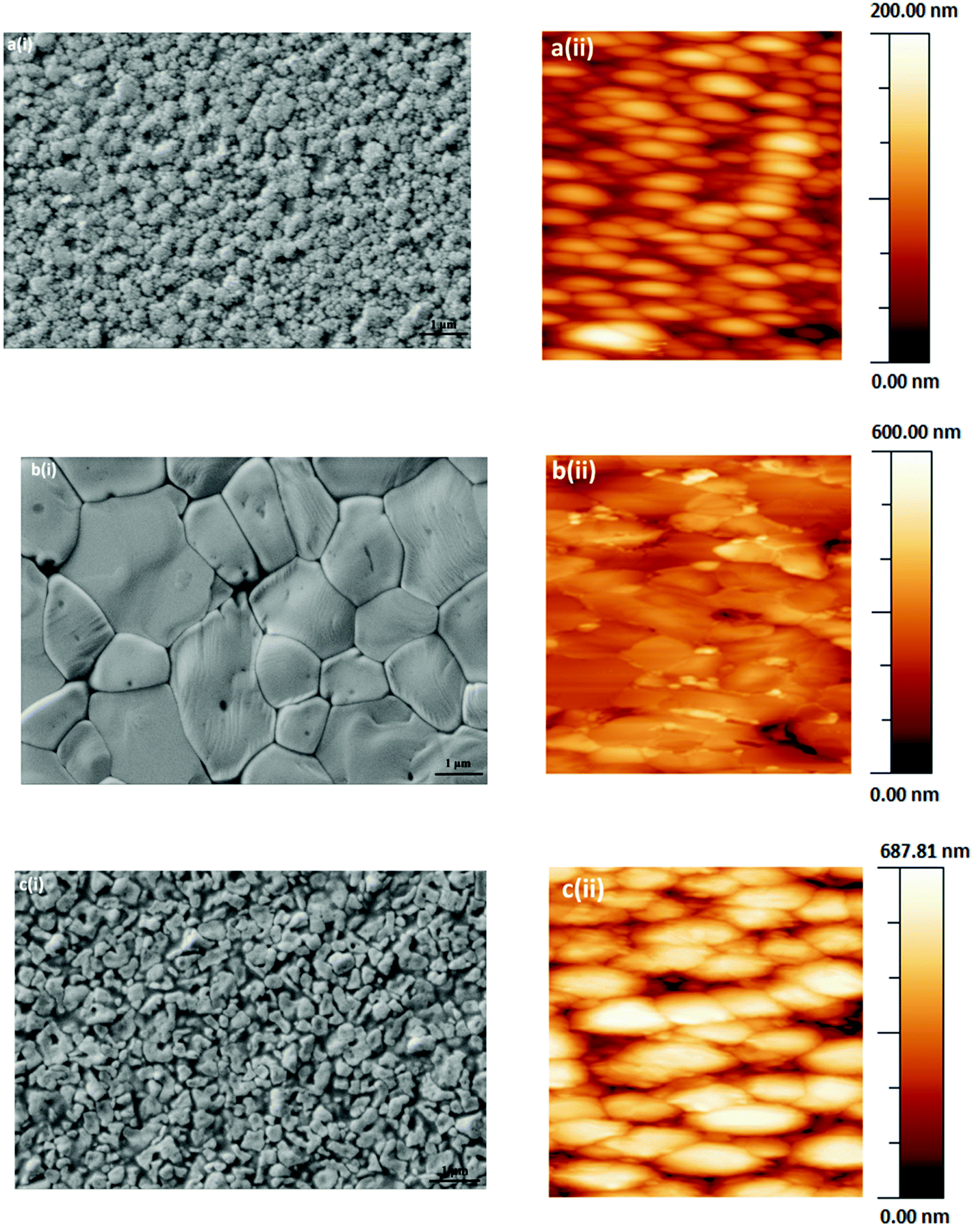 | ||
| Fig. 1 Microscopic characterization of perovskite films. Scanning electron microscopy images (i) on glass/ITO/PEDOT:PSS of (a) MAPbI3, (b) MAPbI3−xClx and (c) MAPbI3−xBrx and their respective atomic force microscopy images (ii). | ||
The exact effect of chloride in terms of modifying the crystallinity of the perovskite morphology is not known.33 In order to probe for the presence and content of chloride within the fabricated MAPbI3−xClx films, energy dispersive X-ray spectroscopy (EDX) measurements were conducted (Fig. S2a, ESI†). However, no hint for the presence of chloride could be found indicating that the concentration is below the detection limit of EDX. The morphological evolution of the MAPbI3−xClx perovskite film may be attributable to slow crystallization induced by the replacement of Cl− with I− during the perovskite formation.8 In contrast to the absence of chloride peaks in the EDX data of CH3NH3PbI3−xClx system, the presence of bromide is observed in the CH3NH3PbI3−xBrx films (Fig. S2b, ESI†). As bromide is heavier than chloride, methylammonium bromide may not be as volatile as methylammonium chloride during the temperature assisted crystallisation and induce defects and imperfection in the perovskite layer resulting in lower power conversion efficiencies of the corresponding photovoltaic devices.
Fig. 2 shows the room temperature absorbance (Fig. 2a) and photoluminescence (PL) spectra (Fig. 2b) of MAPbI3−xYx (Y = Cl, Br, I). The absorption onset for all 3 systems is about 800 nm suggesting highly iodide-dominated perovskite systems even in the case of the mixed-halide formulations. This is consistent with the EDX-findings for MAPbI3−x, the low bromide content in the MAPbI3−xBrx (xstart = 0.2) formulation, and previously reported data on thin films of solution-processed mixed halide perovskites.34–36 Substitution of iodine with chlorine or bromine atoms is expected to increase the band gap of perovskites.37 The PL peak for all three invested formulations occurs in the range of the position reported for MAPbI3.38 This again appears consistent with low chloride and bromide content in the respective film.
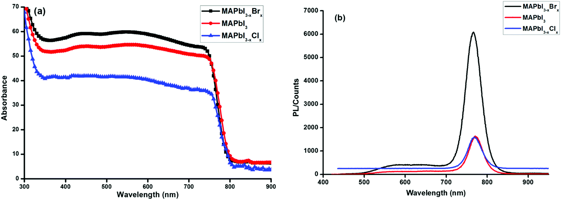 | ||
| Fig. 2 Absorbance (a) and photoluminescence spectra (b) of MAPbI3−xYx (Y = Cl, Br, I) perovskite films on glass. | ||
The impact of the PEDOT:PSS hole transport and the PCBM electron transport interlayer on the dissociation of excitons into free charges and the extraction of free carriers could be estimated by means of photoluminescence spectroscopy. Significant quenching effects were observed from the photoluminescence data of perovskite films in contact with either a PEDOT:PSS or PCBM layer (Fig. S3, ESI†). The quenching of the perovskite PL in the glass/ITO/PEDOT:PSS/perovskite configuration is distinct, and in the glass/ITO/PEDOT:PSS/perovskite/PCBM assembly the quenching becomes quantitative suggesting charge separation to occur at both interfaces, PEDOT:PSS/perovskite and perovskite/PCBM. The data indicate that the carrier generation at the perovskite/PEDOT:PSS interface is less pronounced than at the perovskite/PCBM interface.
3.2 Temperature-dependent photoluminescence spectroscopy
Charge-carrier–phonon interactions, which greatly impact the efficiency of exciton dissociation and charge transfer of the MAPbI3−xYx (Y = Cl, Br, I) systems were elucidated via temperature-dependent photoluminescence spectroscopy. Temperature-dependent PL measurements from 77 to 293 K on perovskite samples on glass substrates were carried out and the data are summarized in Fig. 3. MAPbI3−xYx (Y = Cl, Br, I) perovskite systems show a decrease in emitted photoluminescence intensity with increasing temperature, which is attributed to temperature-activated exciton dissociation.9,39,40 The PL peak of all three materials shows a continuous shift towards higher energy with increasing temperature. The shifts in peak energy at various temperatures may be associated with phase transitions commonly found in lead halide perovskites41,42 or by recently documented increasing the bandgaps of halide perovskite semiconductors upon decreasing the temperature.43 In addition, a significant peak broadening with increasing temperature is observed for MAPbI3 (Fig. 3a) and MAPbI3−xClx (Fig. 3b), both systems showing highly resembling results. In the MAPbI3−xBrx film this peak broadening is distinctively more pronounced (Fig. 3c). The PL broadening is attributed to stronger exciton–phonon interaction at rising temperatures.39,44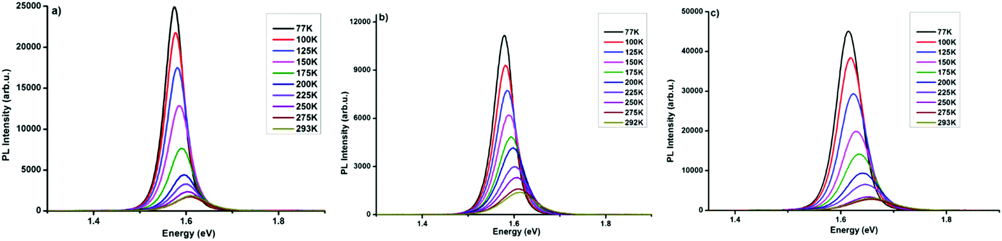 | ||
| Fig. 3 Temperature-dependent photoluminescence spectra recorded at defined temperatures (from 77 K to 293 K) of (a) MAPbI3, (b) MAPbI3−xClx, and (c) MAPbI3−xBrx. | ||
Several groups have reported multi-peak emission behaviour from methylammonium lead halide systems at temperatures below 150 K.40,45–49 The origin of this multi-peak behaviour is not fully understood. Such behaviour was not observed in our MAPbI3−xYx (Y = Cl, Br, I) perovskites. The temperature-dependent photoluminescence data in Fig. 3 were used to assess the linewidth parameters of the fabricated MAPbI3−xYx (Y = Cl, Br, I) perovskites, and the extracted fitting parameters are presented in Fig. 4. As shown in Fig. 4a–c(i), the peak energy changes almost linearly with temperature. Bandgap energies of 1.56, 1.56 and 1.6 eV were extracted for MAPbI3, MAPbI3−xClx and MAPbI3−xBrx, respectively, in good agreement with previous and current reports.3,50,51
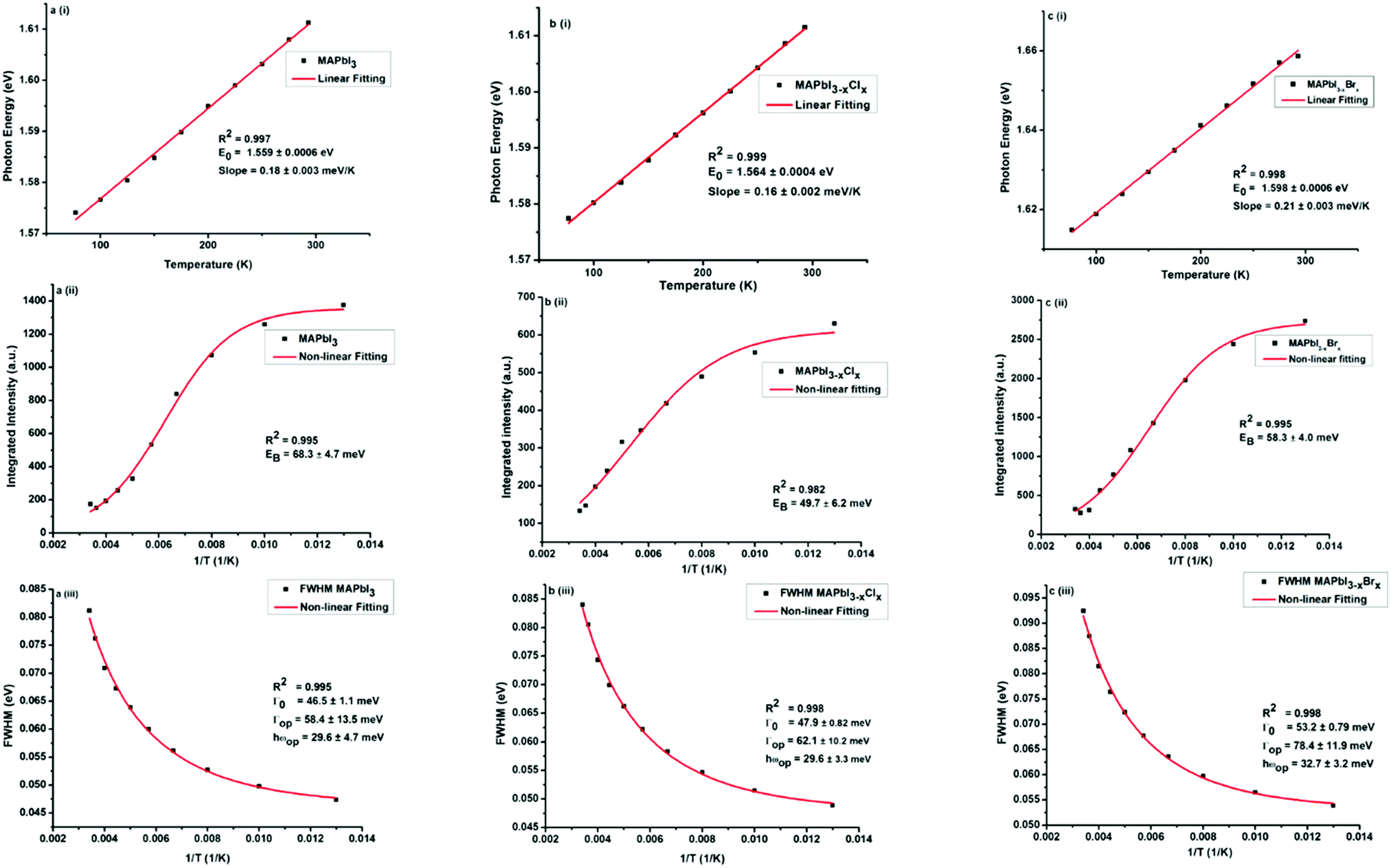 | ||
| Fig. 4 Temperature-dependent photoluminescence linewidth parameters of MAPbI3−xYx (Y = Cl, Br, I) perovskite films: (a) MAPbI3, (b) MAPbI3−xClx and (c) MAPbI3−xBrx: (i) peak energy, (ii) integrated intensity and (iii) temperature-dependent of the full width at half maximum (FWHM). The solid lines represent a linear fit (i) and exponential fits (ii and iii), respectively, of the data points. | ||
The temperature-dependent photoluminescence intensity plotted in Fig. 4a–c(ii), was fitted using the Arrhenius equation,39,52eqn (1),
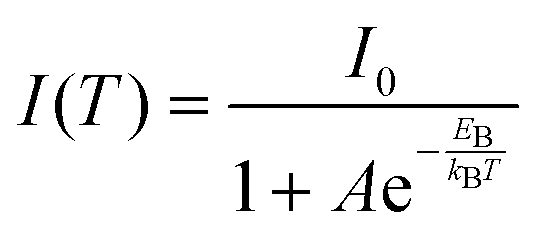 | (1) |
In general, substitution doping of Cl− or Br− into MAPbI3 may hinder collective molecular motions, leading to larger exciton binding energy. However, our results show a decrease in exciton binding energy for both of the mixed halide perovskites in comparison to MAPbI3. From the plots in Fig. 4a–c(ii), a fit of the data points using eqn (1), extracts exciton binding energies (EB) of 68.3 ± 4.7, 49.7 ± 6.2 and 58.3 ± 4.0 meV for MAPbI3, MAPbI3−xClx and MAPbI3−xBrx, respectively, which are within the range of previously reported values.53,54 Similar exciton binding values were reported by Tanaka et al. (∼50 meV for MAPbI3),53 D'Innocenzo et al. (55 ± 20 meV for MAPbI3−xClx),54 and Wu et al. (62.3 ± 8.9 meV for MAPbI3−xClx).40 Other studies using the same Boltzmann activation approach to fit data extracted exciton binding energies of 19 meV9 and 32 meV39 for MAPbI3 and 62 meV40 for MAPbI3−xClx. To the best of our knowledge exciton binding energy values have only been reported for methylammonium lead tribromide perovskites (EB(MAPbBr3) = 60 meV)55 and not for methylammonium lead iodide–bromide perovskites. Exciton binding energies reported in literature cover a broad range from 2 to 55 meV.9,53–60 This rather large variation in exciton binding energy in organic halide lead perovskites is not well understood from fundamental principles. They suggest that the exciton characteristics of hybrid perovskites are sensitive to the synthesis, composition and morphology as shown in our results.
To assess the contributions from phonons the temperature-dependence of the full width at half maximum (FWHM) of the PL was analysed, Fig. 4a–c(iii). From the non-linear fittings of Fig. 4a–c(iii), the gradient of the FWHM versus temperature approaches zero at low temperatures, suggesting negligible exciton–acoustic contribution, σ = 0. The temperature-dependent peak-width broadening was fitted using the independent Boson model:61
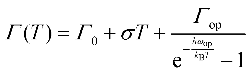 | (2) |
Assuming no exciton–acoustic phonon interaction, as reported in previous temperature-dependent photoluminescence studies40,62 and that photoexcitation results only in radiative luminescence or in charge carriers, fitting of the temperature-dependent photoluminescence data parameters, enabled us to deduce the charge yield, as a function of temperature given by the solid line in Fig. 4a–c(iii). The inhomogeneous broadening contributions, Γ0, for MAPbI3, MAPbI3−xClx and MAPbI3−xBrx were found to be 46.5 ± 1.1, 47.9 ± 0.82 and 53.2 ± 0.79 meV respectively. The exciton–optical phonon contributions, Γop, were found to be 58.4 ± 13.5, 62.1 ± 10.2 and 78.4 ± 11.9 meV respectively. The optical-phonon energies, ℏωop, were determined to be 29.6 ± 4.7, 29.6 ± 3.3 and 32.7 ± 3.2. The values of temperature-dependent FWHM, which were extracted from the data of the MAPbI3−xBrx perovskite system, are somewhat higher than those for MAPbI3 and MAPbI3−xClx. This is attributed to stronger electron–phonon coupling in the bromide perovskite than in the iodide and chloride perovskites.44 The observed inhomogeneous broadening contributions, exciton–optical phonon contribution and optical-phonon energy values are within the range of values reported by Wu et al.40 and Quarti et al.63 (25–42 meV). Although charge-carrier–phonon interactions in methylammonium lead halide perovskites are still a matter of debate, our results provide a link between precursor composition and charge-carrier–phonon interactions.
3.3 Photovoltaic characterization
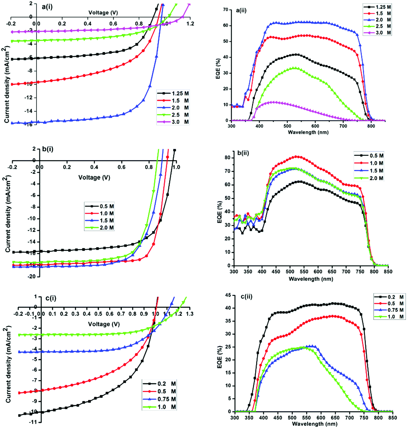 | ||
| Fig. 5 Current density–voltage (J–V) characteristics under AM1.5G illumination and the corresponding EQE spectra of (a) MAPbI3 (MAI = 1.25, 1.5, 2.0, 2.5, 3.0 M), (b) MAPbI3−xClx (MACl = 0.5, 1.0, 1.5 and 2.0 M) and (c) MAPbI3−xBrx (MABr = 0.25, 0.5, 0.75 and 1.0 M) perovskite solar cell. | ||
The photocurrent and external quantum efficiency of typical devices with different PbI2:xMAI molar ratios of 0.8 (1.25 M), 0.6 (1.5 M), 0.5 (2 M), 0.4 (2.5 M) and 0.3 (3 M) are shown in Fig. 5a(i) and (ii). It was found that a non-stoichiometric precursor solution is critical for the formation of MAPbI3 films and a PbI2:MAI molar ratio of 0.5 resulted in the best performing device. Results in Fig. 5a, indicate that high MAI concentrations act deleteriously in the MAPbI3 device as evidenced by the poor photovoltaic performance of cells. Jsc decreases from 15.7 mA cm−2 (at x = 2) to 2.2 mA cm−2 (at x = 3) while Voc increases only from 0.98 to 1.14 V. The integrated EQE was in good agreement with the short-circuit photocurrent density determined from J–V measurements performed under simulated solar radiation. On the basis of these results, the MAPbI3 solar cell device fabrication was optimized with x fixed at 2 (Fig. 6).
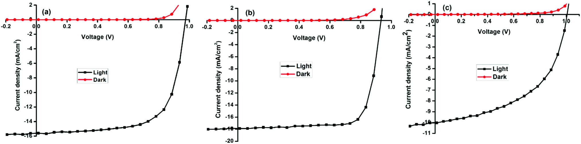 | ||
| Fig. 6 Current density–voltage (J–V) curves of a typical solar cell measured in the dark and under AM1.5 conditions (a) MAPbI3 (b) MAPbI3−xClx (c) and MAPbI3−xBrx. | ||
The J–V curves and external quantum efficiency spectra of typical devices with different MAI:xMACl molar ratios of 2 (0.5 M), 1 (1 M), 0.6 (1.5 M) and 0.5 (2 M) are shown in Fig. 5b(i) and (ii). The trend in PCE as a function of x shows that Jsc decreases from 17.8 mA cm−2 (at x = 1) to 15.6 mA cm−2 (at x = 0.5). Voc increases from 0. 940 V to 0.978 V. On the basis of these results, the MAPbI3−xClx solar cell device fabrication was optimized with x fixed at 1 to enhance the photovoltaic performance of the solar cells. During the rise of Voc with a decrease in x (Fig. 5b(i)), Jsc maintains a relatively large value. It was found that overstoichiometric MACl does not strongly influence the optical properties and photovoltaic performance of the MAPbI3−xClx in contrast to MAPbI3-based solar cells.
Fig. 5c shows the J–V curves for different typical MAPbI3−xBrx photovoltaic devices. The photocurrent and external quantum efficiency spectra of devices with different MAI:xMABr molar ratios of 4 (0.25 M), 1 (1 M), 0.6 (1.5 M) and 0.5 (2 M) are shown in Fig. 5c(i) and (ii). Devices exhibit considerably lower Jsc, Voc, and FF with an increase in x. The trend in PCE as a function of x shows that Jsc decreases from 9.6 mA cm−2 (at x = 0.2) to 2.8 mA cm−2 (at x = 1). In this range Voc increases from 0.98 to 1.22 V. A significant decrease in cell efficiency is observed by increasing the Br content due to a decrease in the Jsc, which is ascribed to the blue shift of the absorption band-edge observed in Fig. 5c(ii). For x > 0.8, the device performance deteriorates considerably.
The best performing halide ratios were compared employing ITO/PEDOT:PSS/perovskite/PCBM/Al planar heterojunction architecture. Representative photovoltaic parameters showing the J–V curves of optimized solar cells measured in the dark and under illumination AM1.5G for MAPbI3, MAPbI3−xClx and MAPbI3−xBrx (Fig. 6). The corresponding semi-logarithmic current–voltage characteristics are shown in Fig. S4 (ESI†). Power conversion efficiencies of 9.2, 12.5 and 5.4% were obtained for MAPbI3, MAPbI3−xClx and MAPbI3−xBrx respectively.
Despite the higher open circuit voltages found for MAPbI3 and MAPbI3−xBrx, devices, power conversion efficiencies are smaller compared to MAPbI3−xClx-based devices due to lower short circuit currents and fill factors. Higher series resistances were observed in MAPbI3 and MAPbI3−xBrx devices compared to MAPbI3−xClx devices. The high FF in MAPbI3−xClx indicates that the charge transport and collection is more efficient, corroborating results obtained in the temperature-dependent photoluminescence spectroscopy. The observed correlation of photovoltaic performance with the mean crystallite size is likely due to the fact that larger perovskite crystallites exhibit a reduced area of grain boundaries and consequently lower overall density of defect states.
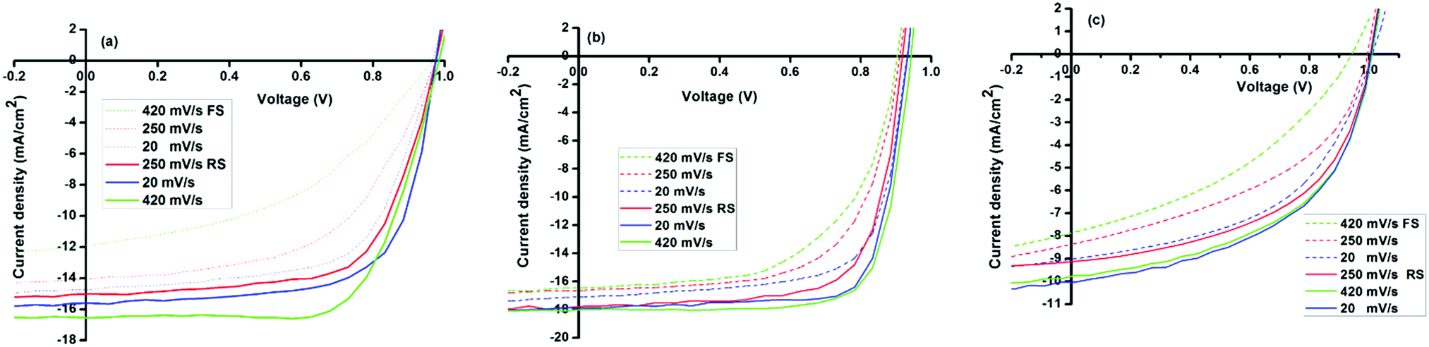 | ||
| Fig. 7 Scan rate- and direction dependent forward and reverse J–V scans of ITO/PEDOT:PSS/MAPbX3/PCBM/Al solar cells (a) PbMAI3, (b) PbMAI3−xClx and (c) PbMAI3−xBrx. | ||
A general trend was observed concerning the influence of the scan rate on hysteresis. Specifically, our results show that the hysteresis is enhanced at high sweep rates and the PCE under reverse scan increases with increases in scan rate, whereas the efficiency under forward scan decreases with the scan rate. Furthermore, the magnitude of the hysteresis is clearly sensitive to the precursors utilized for the perovskite growth as it is minimal in PbMAI3−xClx solar cells compared to their PbMAI3 and PbMAI3−xBrx counterparts.
Hysteresis in perovskite-absorber devices has been speculated to originate from ion migration.66–68 Since ion migration is particularly sensitive to the concentration of mobile vacancies, this would suggest that the hysteretic behaviour of perovskite devices should be influenced by the stoichiometry of the perovskite material, as well as the degree of crystallinity and the size of crystalline domains. We therefore investigated concentration-dependent hysteretic behaviour of the prepared perovskite solar cells. Fig. S6 (ESI†) shows that hysteresis is most severe at high MAX concentrations with less hysteresis in MAPbI3−xClx in comparison to MAPbI3 and MAPbI3−xBrx devices. However, the origin of the J–V hysteresis is still under debate and there are challenges associated with the proposed mechanisms.
The statistical data analysis of the investigated devices is shown in Fig. S7 (ESI†) and device parameters are summarized in Table S1 (ESI†). The data shows that PbMAI3−xClx cells exhibit superior photovoltaic performance in comparison to PbMAI3 and PbMAI3−xBrx devices.
4. Conclusion
In summary, we fabricated low-cost planar heterojunction perovskite solar cells which offer a wide tenability of their composition and structure by adjusting the metal halide framework. We investigated their optical and electronic properties to develop a fundamental understanding of perovskite material properties and device operation principles. Our work shows that methylammonium lead halide perovskites exhibit composition-/structure-dependent properties. Although the exact values for exciton binding energies in methylammonium lead halide perovskites are still a matter of debate, our results fall into the range of reported values and provide a link between composition and charge carrier–phonon interactions. Whether the opto-electrical and photovoltaic performance differences between the single halide (tri-iodide) and mixed halide (I/Cl and I/Br) perovskite materials are a result of crystal orientations or different photogenerated excitations, requires more research.Acknowledgements
Sekai Tombe gratefully acknowledges financial support from L'Oréal-UNESCO For Women in Science Sub-Saharan Africa Fellowship and the National Research Foundation of South Africa (NRF). Getachew Adam acknowledges the Austrian Research Promotion Agency (FFG) (flex!PV 838621, flex!PV_2.0 85360) for financial support. Herwig Heilbrunner acknowledges the Austrian Research Promotion Agency (FFG) (SolarTrap 843929) for financial support. Christoph Ulbricht acknowledges the Austrian Research Promotion Agency (FFG) (3D-MEOD 843685) for financial support. The financial support of Austrian Science Funds (FWF) within the Wittgenstein Prize of Professor Sariciftci is gratefully acknowledged.References
- A. Kojima, K. Teshima, Y. Shirai and T. Miyasaka, J. Am. Chem. Soc., 2009, 131, 6050–6051 CrossRef CAS PubMed.
- J.-H. Im, C.-R. Lee, J.-W. Lee, S.-W. Park and N.-G. Park, Nanoscale, 2011, 3, 4088–4093 RSC.
- W. S. Yang, J. H. Noh, N. J. Jeon, Y. C. Kim, S. Ryu, J. Seo and S. I. Seok, Science, 2015, 348, 1234–1237 CrossRef CAS PubMed.
- NREL http://www.nrel.gov/ncpv/images/efficiency_chart.jpg.
- H. J. Snaith, J. Phys. Chem. Lett., 2013, 4, 3623–3630 CrossRef CAS.
- M. A. Green, K. Emery, Y. Hishikawa, W. Warta and E. D. Dunlop, Prog. Photovoltaics, 2016, 24(7), 905–913 Search PubMed.
- J. H. Noh, S. H. Im, J. H. Heo, T. N. Mandal and S. I. Seok, Nano Lett., 2013, 13, 1764–1769 CrossRef CAS PubMed.
- N. Yantara, F. Yanan, C. Shi, H. A. Dewi, P. P. Boix, S. G. Mhaisalkar and N. Mathews, Chem. Mater., 2015, 27, 2309–2314 CrossRef CAS.
- S. Sun, T. Salim, N. Mathews, M. Duchamp, C. Boothroyd, G. Xing, T. C. Sum and Y. M. Lam, Energy Environ. Sci., 2014, 7, 399–407 CAS.
- S. D. Stranks, G. E. Eperon, G. Grancini, C. Menelaou, M. J. Alcocer, T. Leijtens, L. M. Herz, A. Petrozza and H. J. Snaith, Science, 2013, 342, 341–344 CrossRef CAS PubMed.
- G. Xing, N. Mathews, S. Sun, S. S. Lim, Y. M. Lam, M. Grätzel, S. Mhaisalkar and T. C. Sum, Science, 2013, 342, 344–347 CrossRef CAS PubMed.
- Q. Dong, Y. Fang, Y. Shao, P. Mulligan, J. Qui, L. Cao and J. Huang, Science, 2015, 347, 967–970 CrossRef CAS PubMed.
- D. B. Mitzi, Prog. Inorg. Chem., 2007, 48, 1 CrossRef.
- G. Xing, N. Mathews, S. S. Lim, N. Yantara, X. Liu, D. Sabba, M. Grätzel, S. Mhaisalkar and T. C. Sum, Nat. Mater., 2014, 13, 476–480 CrossRef CAS PubMed.
- A. Sharenko and M. F. Toney, J. Am. Chem. Soc., 2016, 138, 463–470 CrossRef CAS PubMed.
- H. Tsai, W. Nie, P. Cheruku, N. H. Mack, P. Xu, G. Gupta, A. D. Mohite and H.-L. Wang, Chem. Mater., 2015, 27, 5570–5576 CrossRef CAS.
- F. Matsumuto, S. M. Vorpahl, J. Q. Banks, E. Sengupta and D. S. Ginger, J. Phys. Chem. C, 2015, 119, 20810–20816 Search PubMed.
- M. Liu, M. B. Johnston and H. J. Snaith, Nature, 2013, 501, 395–398 CrossRef CAS PubMed.
- D. Liu and T. L. Kelly, Nat. Photonics, 2013, 8, 133–138 CrossRef.
- G. E. Eperon, S. D. Stranks, C. Menelaou, M. B. Johnston, L. Herz and H. J. Snaith, Energy Environ. Sci., 2014, 7, 982–988 CAS.
- J. You, Z. Hong, Y. M. Yang, Q. Chen, M. Cai, T.-B. Song, C.-C. Chen, S. Lu, Y. Liu, H. Zhou and Y. Yang, ACS Nano, 2014, 8, 1674–1680 CrossRef CAS PubMed.
- Q. Chen, H. Zhou, Z. Hong, S. Luo, H.-S. Duan, H.-H. Wang, Y. Liu, G. Li and Y. Yang, J. Am. Chem. Soc., 2014, 136, 622–625 CrossRef CAS PubMed.
- M. M. Lee, J. Teuscher, T. Miyasaka, T. N. Murakami and H. J. Snaith, Science, 2012, 338, 643–647 CrossRef CAS PubMed.
- J. M. Ball, M. M. Lee, A. Hey and H. J. Snaith, Energy Environ. Sci., 2013, 6, 1739 CAS.
- J. T.-W. Wang, J. M. Ball, E. M. Barea, A. Abate, J. A. Alexander-Webber, J. Huang, M. Saliba, I. Mora-Sero, J. Bisquert, H. J. Snaith and R. J. Nicholas, Nano Lett., 2014, 14, 724–730 CrossRef CAS PubMed.
- D. Bi, S.-J. Moon, L. Häggman, G. Boschloo, L. Yang, E. M. J. Johansson, M. K. Nazeeruddin, M. Grätzel and A. Hagfeldt, RSC Adv., 2013, 3, 18762 RSC.
- H.-S. Kim, C.-R. Lee, J.-H. Im, K.-B. Lee, T. Moehl, A. Marchioro, S.-J. Moon, R. Humphry-Baker, J.-H. Yum, J. E. Moser, M. Grätzel and N.-G. Park, Sci. Rep., 2012, 2, 591 Search PubMed.
- J. Burschka, N. Pellet, S.-J. Moon, R. Humphry-Baker, P. Gao, M. K. Nazeeruddin and M. Grätzel, Nature, 2013, 499, 316–319 CrossRef CAS PubMed.
- N. Pellet, P. Gao, G. Gregori, T.-Y. Yang, M. K. Nazeeruddin, J. Maier and M. Grätzel, Angew. Chem., Int. Ed., 2014, 53, 3151–3157 CrossRef CAS PubMed.
- G. Adam, M. Kaltenbrunner, E. D. Głowacki, M. S. White, H. Heilbrunner, S. Tombe, P. Stadler, B. Ernecker, C. W. Klampfl, N. S. Sariciftci and M. C. Scharber, Sol. Energy Mater. Sol. Cells, 2016, 157, 318–325 CrossRef CAS.
- H. Zhou, Q. Chen, G. Li, S. Luo, T. Song, H.-S. Duan, Z. Hong, J. You, Y. Liu and Y. Yang, Science, 2014, 345, 542–546 CrossRef CAS PubMed.
- D. T. Moore, H. Sai, K. W. Tan, D.-M. Smilgies, W. Zhang, H. J. Snaith, U. Wiesner and L. A. Estroff, J. Am. Chem. Soc., 2015, 137, 2350–2358 CrossRef CAS PubMed.
- E. Edri, S. Kirmayer, A. Henning, S. Mukhopadhyay, K. Gartsman, Y. Rosenwaks, G. Hodes and D. Cahen, Nano Lett., 2014, 14, 1000–1004 CrossRef CAS PubMed.
- S. Colella, E. Mosconi, P. Fedeli, A. Listorti, F. Gazza, F. Orlandi, P. Ferro, T. Besagni, A. Rizzo, G. Calestani, G. Gigli, F. De Angelis and R. Mosca, Chem. Mater., 2013, 25, 4613–4618 CrossRef CAS.
- F. Deschler, M. Price, S. Pathak, L. E. Klintberg, D.-D. Jarausch, R. Higler, S. Hüttner, T. Leitjens, S. D. Stranks, H. J. Snaith, M. Atatüre, R. T. Phillips and R. H. Friend, J. Phys. Chem. Lett., 2014, 5, 1421–1426 CrossRef CAS PubMed.
- T. Baikie, J. Mater. Chem. A, 2013, 1, 5628–5641 CAS.
- P. Gao, M. Grätzel, M. K. Nazeeruddin, J. Maier and M. Grätzel, Energy Environ. Sci., 2014, 7, 2448–2463 CAS.
- Y. Yasuhiro, N. Toru, E. Masaru, W. Atsushi and Y. Yoshihiko, Appl. Phys. Express, 2014, 7, 032302 CrossRef.
- T. J. Savenije, C. S. Ponseca, L. Kunneman, M. Abdellah, K. Zheng, Y. Tian, Q. Zhu, S. E. Canton, I. G. Scheblykin, T. Pullerits, A. Yartsev and V. Sundström, J. Phys. Chem. Lett., 2014, 5, 2189–2194 CrossRef CAS PubMed.
- K. Wu, A. Bera, C. Ma, Y. Du, Y. Yang, L. Li and T. Wu, Phys. Chem. Chem. Phys., 2014, 16, 22476 RSC.
- C. C. Stoumpos, C. D. Malliakas and M. G. Kanatzidis, Inorg. Chem., 2013, 52, 9019–9038 CrossRef CAS PubMed.
- H.-H. Fang, F. Wang, S. Adjokatse, N. Zhao, J. Even and M. A. Loi, Light: Sci. Appl., 2016, 5, e16056 CrossRef CAS.
- W. L. Leong, Z.-E. Ooi, D. Sabba, C. Yi, S. M. Zakeeruddin, M. Graetzel, J. M. Gordon, E. A. Katz and N. Mathews, Adv. Mater., 2016, 28, 2439–2445 CrossRef CAS PubMed.
- A. D. Wright, C. Verdi, R. L. Milot, G. E. Eperon, M. A. Pérez-Osorio, H. J. Snaith, F. Giustino, M. B. Johnston and L. M. Herz, Nat. Commun., 2016, 7, 11755 Search PubMed.
- R. L. Milot, G. E. Eperon, H. J. Snaith, M. B. Johnston and L. M. Herz, Adv. Funct. Mater., 2015, 25, 6218–6227 CrossRef CAS.
- M. Karakus, S. A. Jensen, F. D'Angelo, D. Turchinovich, M. Bonn and M. Cánovas, J. Phys. Chem. Lett., 2015, 6, 4991–4996 CrossRef CAS PubMed.
- H.-H. Fang, R. Raissa, M. Abdu-Aguye, S. Adjokatse, G. R. Blake, J. Even and M. A. Loi, Adv. Funct. Mater., 2015, 25, 2378–2385 CrossRef CAS.
- X. Wu, M. T. Trinh, D. Niesner, H. Zhu, Z. Norman, J. S. Owen, O. Yaffe, B. J. Kudisch and X.-Y. Zhu, J. Am. Chem. Soc., 2015, 137, 2089–2096 CrossRef CAS PubMed.
- D. Priante, I. Dursun, M. S. Alias, D. Shi, V. A. Melnikov, T. K. Ng, O. F. Mohammed, O. M. Bakr and B. S. Ooi, Appl. Phys. Lett., 2015, 106, 081902 CrossRef.
- S. A. Kulkarni, T. Baikie, P. P. Boix, N. Yantara, N. Mathews and S. G. Mhaisalkar, J. Mater. Chem. A, 2014, 2, 9221 CAS.
- S. M. H. Qaid, M. S. Al Sobaie, M. A. M. Khan, I. M. Bedja, F. H. Alharbi, M. K. Nazeeruddin and A. S. Aldwayyan, Mater. Lett., 2016, 164, 498–501 CrossRef CAS.
- Z. Chen, C. Yu, K. Shum, J. J. Wang, W. Pfenninger, N. Vockic, J. Midgley and J. T. Kenney, J. Lumin., 2012, 132, 345–349 CrossRef CAS.
- K. Tanaka, T. Takahashi, T. Ban, T. Kondo, K. Uchida and N. Miura, Solid State Commun., 2003, 127, 619–623 CrossRef CAS.
- V. D'Innocenzo, G. Grancini, M. J. P. Alcocer, A. R. S. Kandada, S. D. Stranks, M. M. Lee, G. Lanzani, H. J. Snaith and A. Petrozza, Nat. Commun., 2014, 5, 3586 Search PubMed.
- N. Sestu, M. Cadelano, V. Sarritzu, F. Chen, D. Marongiu, R. Piras, M. Mainas, F. Quochi, M. Saba, A. Mura and G. Bongiovanni, J. Phys. Chem. Lett., 2015, 6, 4566–4572 CrossRef CAS PubMed.
- M. Hirasawa, T. Ishihara, T. Goto, K. Uchidaand and N. Miura, Phys. B, 1994, 201, 427–430 CrossRef CAS.
- E. Menéndez-Proupin, P. Palacios, P. Wahnón and J. C. Conesa, Phys. Rev. B: Condens. Matter Mater. Phys., 2014, 90, 045207 CrossRef.
- J. Even, L. Pedesseau and C. Katan, J. Phys. Chem. C, 2014, 118, 11566–11572 CAS.
- A. Miyata, A. Mitioglu, P. Plochocka, O. Portugall, J. T.-W. Wang, S. D. Stranks and R. J. Nicholas, Nat. Phys., 2015, 11, 582–587 CrossRef CAS.
- L. M. Herz, Annu. Rev. Phys. Chem., 2016, 67, 65–89 CrossRef CAS PubMed.
- S. Rudin, T. L. Reinecke and B. Segall, Phys. Rev. B: Condens. Matter Mater. Phys., 1990, 42, 11218–11231 CrossRef CAS.
- B. Zhang, T. Taliercio, S. Kolliakos and P. Lefebvre, J. Phys.: Condens. Matter, 2001, 13, 7053–7074 CrossRef.
- C. Quarti, G. Grancini, E. Mosconi, P. Bruno, J. M. Ball, M. M. Lee, H. J. Snaith, A. Petrozza and F. De Angelis, J. Phys. Chem. Lett., 2013, 5, 279–284 CrossRef PubMed.
- J. Wei, Y. C. Zhao, H. Li, G. B. Li, J. L. Pan, D. S. Xu, Q. Zhao and D. P. Yu, J. Phys. Chem. Lett., 2014, 5, 3937–3945 CrossRef CAS PubMed.
- B. C. O'Regan, P. R. F. Barnes, X. Li, C. Law, E. Palomares and J. M. Marin-Beloqui, J. Am. Chem. Soc., 2015, 137, 5087–5099 CrossRef PubMed.
- A. Dualeh, T. Moehl, N. Tétreault, J. Teuscher, P. Gao, M. K. Nazeeruddin and M. Grätzel, ACS Nano, 2014, 8, 362–373 CrossRef CAS PubMed.
- H. J. Snaith, A. Abate, J. M. Ball, G. E. Eperon, T. Leitjens, N. K. Noel, S. D. Stranks, J. T.-W. Wang, K. Wojciechowski and W. Zhang, J. Phys. Chem. Lett., 2014, 5, 1511–1515 CrossRef CAS PubMed.
- E. L. Unger, E. T. Hoke, C. D. Bailie, W. H. Nguyen, A. R. Bowring, T. Heumüller, M. G. Christoforo and M. D. McGehee, Energy Environ. Sci., 2014, 7, 3690 CAS.
Footnote |
| † Electronic supplementary information (ESI) available. See DOI: 10.1039/c6tc04830g |
| This journal is © The Royal Society of Chemistry 2017 |