
 Open Access Article
 This Open Access Article is licensed under a Creative Commons Attribution-Non Commercial 3.0 Unported Licence
Modulation doping of transition metal dichalcogenide/oxide heterostructures†
Kang
Xu
,
Yi
Wang
,
Yuda
Zhao
and
Yang
Chai
*
Department of Applied Physics, The Hong Kong Polytechnic University, Hung Hom, Kowloon, Hong Kong, P. R. China. E-mail: ychai@polyu.edu.hk
First published on 2nd December 2016
Abstract
Control of carrier type and carrier density provides a way to tune the physical properties of two-dimensional (2D) semiconductors. Modulation doping of heterostructures can effectively inject carriers into or extract carriers from the 2D semiconductors, and eliminate the adverse effect from the ionized dopants. Here we first investigate the layer-dependent negative trion PL of 2D MoS2, and further construct heterostructures with transition metal dichalcogenides (TMDs) and transition metal oxides (TMOs). By choosing the oxide with different charge neutrality levels (CNLs), we demonstrate effective electron injection into MoS2 by TiO2 doping, and electron extraction from MoS2 by MoO3 doping. Photoluminescence (PL) spectra and electrical characterization show that thicker MoS2 flakes are more easily n-doped by TiO2, while thinner MoS2 flakes are more easily p-doped by MoO3. Our experimental results are in good agreement with theoretical calculations. The modulation doping with TMO is compatible with conventional Si processing and highly air-stable. This method can also be extended for the controllable doping of other 2D materials.
Introduction
Two-dimensional (2D) layered transition metal dichalcogenides (TMDs) are of great research interest because of their unique electronic, optical and optoelectronic properties.1–5 The modulation of carrier density in the TMDs provides a way to change their physical properties in a controllable manner. For typical TMD materials, the pristine carrier type is predominated by their intrinsic characteristics. For example, pristine MoS2 is of the n-type while WSe2 shows p-type or ambipolar characteristics (the carrier type of WSe2 is dependent on its thickness).2,6–8 Controllable injection and extraction of electrons/holes are important for effective n- and p-doping of TMDs, which are crucial for building complementary logic circuits in the future. On the other hand, the interaction between carriers and excitons enables an additional path for the PL modulation of 2D layered materials. Controlling the carrier type and density through modulation doping provides a way to switch between exciton- and trion-dominant PL and tune the PL intensity of 2D materials.9Various methods have been developed to dope 2D layered TMDs,10 including substitutional doping during growth,11 ion implantation,12 plasma treating,13etc. Although these doping methods have been demonstrated to be effective, they inevitably result in the distortion of TMD crystal structures, introduce ionized impurity scattering canters, and degrade the charge mobility. Modulation doping has been widely used in III–V compound heterojunction superlattices to eliminate the influence of ionized impurity scattering.14–16 In the heterojunction device, the ionized dopants and electrons are confined to two different adjacent layers. As a result, both the mobility and carrier concentration are well maintained. A variety of dopants have been studied for the surface charge transfer to TMDs, including gas molecules,17 organics,18 metal particles19 and oxides.2,20 Among these kinds of dopants, oxide is one of the promising species due to its stability in ambience and compatibility with conventional Si processing technology.
In this work, we deposit transition metal oxide (TMO) on top of 2D MoS2 to form a heterojunction device. We choose TiO2 with a high charge neutrality level (CNL) and MoO3 with a low CNL for injecting and extracting electrons, respectively. Our optical and electrical characterization, together with density functional theory (DFT) calculations, shows that TiO2 and MoO3 deposition gives rise to effective n-doping and p-doping, respectively. In addition, we also reveal layer-dependent negative trion photoluminescence (PL) and doping effects in 2D layered MoS2. This approach opens up a way to control the characteristics of PL and the electrical transport of 2D layered materials.
Results and discussion
Layer-dependent negative trion PL of 2D MoS2
Because of the extremely strong Coulomb interaction in ultrathin 2D MoS2, optically generated excitons (i.e., electron–hole pairs) and trions (i.e., charged excitons) can exist stably at room temperature.21 Electrons are excited to the conducting band, leaving holes in the valence band. Electrons and holes are then bound together by Coulomb interactions to form neutrally charged excitons (electron–hole pairs). Due to the Coulomb attraction between the hole in an exciton and a third electron, the formation process of exciton to trion is energy favourable.22 Trions are formed in the presence of residual free charges. Fig. 1(a) shows the PL spectra of a 3L MoS2 as an example. Two pronounced peaks around 1.87 eV and 2.05 eV are clearly observed, defined as the A exciton peak and the B exciton peak, respectively. As schematically depicted in the inset, the A exciton has originated from the radiative recombination of the excited electrons in the conduction band minimum (CBM) with the holes in the valence band minimum (VBM); and the B exciton has originated from the radiative recombination of the excited electrons in the CBM with the lower branch of the split VBM.23 The A exciton of ultrathin MoS2 can be further devolved into a neutron exciton (X) peak around 1.9 eV and a negative trion (X−) peak around 1.85 eV.21 | ||
| Fig. 1 PL analysis of ultrathin MoS2 flakes. (a) PL spectrum of 3L MoS2. The inset shows the radiative recombination path of A and B excitons, respectively. (b) PL spectra of 1L–4L MoS2. (c) Layer-dependent spectral weight of the X− peak. (d) Layer-dependent photon energy of the X peak and the X− peak in the MoS2 samples from 1L to 5L. The inset shows the layer-dependent energy difference between the X peak and the X− peak. | ||
Fig. 1(b) shows the PL spectra of MoS2 evolved with the layer number from 1L to 4L. The PL spectra of over 60 MoS2 flakes were collected and are summarized in Fig. 1(c) and (d). Fig. 1(c) shows the layer-dependent spectral weight of the X− peak in the whole A exciton peak, which rapidly decreases from 90% in the 1L MoS2 to 30% in the 3L–5L MoS2. There are two possible reasons accounting for the layer-dependent characteristic of the spectral weight of the X− peak. First, electrons in MoS2 originated from donor states introduced by surface sulfur vacancies,24–27 which are expected to become less prominent with the increase of body thickness. Second, when the thickness of MoS2 increases, the dielectric screening of MoS2 increases,28,29 which attenuates the Coulomb interaction30 and reduces the binding energy of trions. With the decrease of binding energy, trion systems are less stable and can be easily decomposed into excitons. Fig. 1(d) shows the photon energy of X and X− peaks as a function of MoS2 thickness. The PL peaks exhibit a clear red-shift with an increase of MoS2 body thickness due to the decreased bandgap. In the inset of Fig. 1(d), we present the layer-dependent energy difference (binding energy of the negative trion from the exciton) between X and X− peaks. This binding energy decreases with the increase of MoS2 thickness.
Layer-dependent n-doping of MoS2 by TiO2
Fig. 2 shows the PL spectra of 1L–4L MoS2 before and after TiO2 deposition. After 6 nm thick Atomic Layer Deposition (ALD) TiO2 doping, we observe the characteristics of layer-dependent PL. The thicker MoS2 sample has a smaller X− spectral weight before the TiO2 deposition, which is consistent with our previous discussions; while the X− spectral weight increases more after the TiO2 deposition. These changes in PL spectra are ascribed to the injection of electrons from TiO2 into MoS2, where the electron density in MoS2 is increased by TiO2 doping.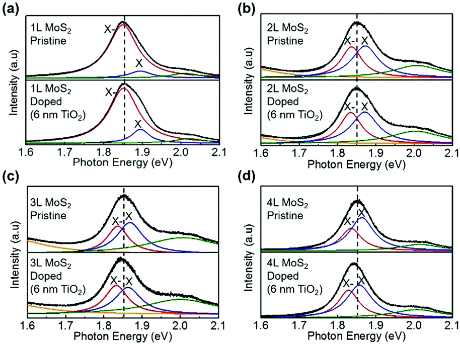 | ||
| Fig. 2 PL spectra of ultrathin MoS2 flakes before and after depositing 6 nm thick TiO2. The thicknesses of MoS2 samples are (a) 1L, (b) 2L, (c) 3L and (d) 4L. | ||
To rule out the possibility that this PL change has originated from in-plain lattice strain due to oxide deposition on the surface, we also present the corresponding Raman spectra before and after doping in Fig. S1 (ESI†). As widely reported by previous research studies, the in-plane lattice strain induces the split of the E12g peak and the blue-shift of both E12g and A1g peaks.31 However, from our Raman spectra, we observe no such Raman spectral change. Thus, it is suggested that the interlayer coupling between the TiO2 layer and the MoS2 surface is very weak, and this weak interaction induces negligible lattice strain to MoS2. So the PL spectral change has not originated from the lattice strain. To confirm this speculation, we further deposited 30 nm thick TiO2 onto 1L–3L MoS2. The Raman and PL spectra are shown in Fig. S2 (ESI†). We still observe a more significant increase of the X− spectral weight in thicker MoS2 and a negligible shift of Raman peaks. It is noteworthy that the attenuation of Raman intensity after the doping is possibly due to the block of light of the 30 nm thick TiO2 layer. On the other hand, the change of the dielectric environment introduced by TiO2 deposition plays an important role in the change of the PL spectra of MoS2. In both cases (6 nm thick and 30 nm thick TiO2), the A exciton peak is found to be red-shifted after the TiO2 deposition, which is more obvious in the case of 30 nm thick TiO2 deposition. This is because the bandgap of MoS2 is decreased in the environment with a higher dielectric constant (the dielectric constant of TiO2 is ∼80).30 Furthermore, from the point of view of enhanced dielectric screening in MoS2 due to the deposition of the TiO2 layer, the Coulomb interaction in MoS2 is attenuated (similar to the effect of increasing MoS2 body thickness). The attenuated Coulomb interaction decreases the binding energy of the negative trion, thus decreasing the stability of the trion system and the PL intensity of the X− peak. However, in our experiments, the PL intensity of the X− peak is obviously increased after the TiO2 doping. Therefore, the increase of the X− peak PL is due to the increase of electron density in MoS2, which originated from the n-doping effect by TiO2.
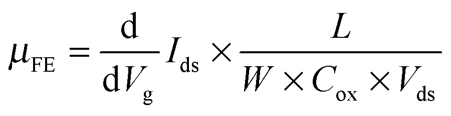
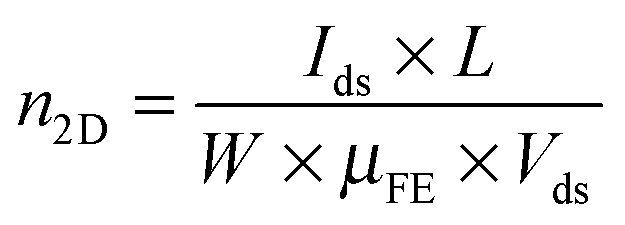
To further confirm and quantify the n-doping effect, we fabricated a back-gated MoS2 field effect transistor (FET) and doped it with 6 nm thick ALD TiO2. Fig. 3(a) depicts the cross-sectional schematic of a back-gated MoS2 FET with its channel covered by TMO. Fig. 3(b) shows the transfer curve of a 5L MoS2 FET before (black line) and after (red line) the 6 nm thick TiO2 doping. The pristine device shows typical n-type behaviour, consistent with previous reports.1,32 After n-doping, the ON current (ION) is increased by a factor of 4 at Vbg = 50 V. Fig. 3(c) and (d) show the output curves of the same device before and after doping, respectively. Again, ION at Vbg = 50 V is found to be amplified about 5 times. It is noteworthy that the device retains its semiconducting characteristics after the doping, indicating that the n-doping effect is non-degenerate. Furthermore, we can extract 2D sheet carrier density (n2D) and field-effect mobility (μFE) according to eqn (1) and (2), where L and W are the channel length and the channel width, respectively, and Cox is the capacitance of the gated oxide (i.e., 1.16 × 10⁻⁸ F cm−2 for 300 nm thick SiO2 in this study).1 The extracted n2D before doping is 1.17 × 1012 cm−2, which is consistent with previous reports,32–35 while the extracted n2D after the doping is 1.95 × 1012 cm−2. This doping level (0.78 × 1012 cm−2) is comparable with other doping methods (i.e., 2 × 1011 cm−2 for OTS-doped WSe2,36 4.6 × 1011 cm−2 for MEA-doped MoS2,37 −2 × 1011 cm−2 for FDT-doped MoS2,34 and 1 × 1013 cm−2 for TiOx-doped graphene).37 The μFE and n2D are extracted at Vbg = 30 V. Although the doping effect is independent of the back gate voltage, sufficient gate voltage is required to turn on the channel of the device. It is noteworthy that in these devices, the charges are free carriers without the formation of excitons or trions. Because there is no external input to excite electrons to the conduction band and the lifetimes of excitons and trions are very short, in the order of picoseconds,38,39
 | (1) |
 | (2) |
 | ||
| Fig. 3 Electrical characterization of a MoS2 FET for n-doping by TiO2. (a) Cross-sectional schematic of a TMO doped MoS2 FET. (b) Transfer curve of a 5L MoS2 FET before (black line) and after (red line) being doped by 6 nm thick TiO2. (c) Output curves of the FET before doping; (d) output curves of the FET after doping. | ||
To further support our findings, DFT calculations were utilized to simulate the doping effect. The anatase phase TiO2 structure was used in this simulation since it is a stable phase at a relatively low temperature.20Fig. 4(a) and (b) show the atomic and orbital projected density of states of pristine 1H-MoS2, 1H-MoS2 in the TiO2-doped MoS2 system, anatase TiO2, and anatase TiO2 in the TiO2-doped MoS2 system. The bandgap of pristine 1H-MoS2 is calculated to be ∼1.86 eV. And both the conduction band minimum (CBM) and the valence band maximum (VBM) of MoS2 are populated by the 4d orbital of the Mo atom, which are highly hybridized with the 3p orbital of the S atom.20 After the TiO2 doping, the Fermi level of 1L MoS2 is up-shifted approximately 0.76 eV towards the CBM, indicating the n-doping effect. Also, the bandgap of MoS2 is obviously shrunken, which is due to the enhanced dielectric screening introduced by TiO2 deposition. From Fig. 4(b), we observe a significant change in the DOS of TiO2 after the n-doping. Compared with the pristine state, the presence of the Ti-5d level in the conduction band is dramatically decreased. This change indicates that electrons are mainly transferred from the Ti-5d level of TiO2 to MoS2, leaving the Ti-5d level anti-bonding. Similar findings regarding the simulation of the TiO2 doping process can be found in the work of N. Kaushik et al.40
 | ||
| Fig. 4 DFT simulation results of the n-doping process and band structures of MoS2 and TiO2. (a) DOS of 1L 1H-MoS2 before (upper panel) and after doping (lower panel). (b) DOS of anatase TiO2 before (upper panel) and after doping MoS2 (lower panel). (c) Band alignment of 1L MoS2 and TiO2 before doping. (d) Band alignment of 1L MoS2 and TiO2 after doping. The dashed lines denote the CNL. | ||
Fig. 4(c) shows the schematic band structures of 1L MoS2versus anatase TiO2. The CBM and CNL of MoS2 are about 0.5 eV lower than those of TiO2. Driven by this energy difference, electrons in the CB of TiO2 flows into the CB of MoS2, until an interface dipole pointing from MoS2 to TiO2 is built up (Fig. 4(d)) and then the doping process reaches its balance state. As widely acknowledged, electrons in ultrathin MoS2 flakes have originated from surface sulfur vacancies. It is reasonable to expect that this surface effect has a smaller influence on the electronic structure of thicker MoS2 samples. The CNL of MoS2 thin flakes lowers when the thickness of MoS2 increases. Considering the fact that the bandgap of MoS2 decreases with the increase of body thickness, the CNL of thicker MoS2 samples quickly lowers down. For thicker MoS2 samples, the energy difference between its CNL and that of TiO2 enlarges, thus the n-doping effect is more obvious.
Layer-dependent p-doping of MoS2 by MoO3
MoO3 is one type of TMOs with a relatively low CNL. We choose it for p-doping MoS2. Fig. 5 shows the PL spectra of 1L and 3L MoS2 before and after 6 nm thick MoO3 doping. In both cases, a significant decrease of the X− peak spectral weight is observed. The corresponding Raman spectra of these samples are shown in Fig. S3 (ESI†). No obvious shift in the positions of Raman peaks is observed, suggesting that the interlayer coupling between the MoO3 layer and the MoS2 surface is also very small. Also, it is noteworthy that the dielectric constant of MoO3 is small (∼5.5). Therefore, it has a negligible influence on the PL spectra of MoS2. | ||
| Fig. 5 PL spectra of ultrathin MoS2 flakes before and after being doped by 6 nm thick MoO3. The thicknesses of MoS2 samples are (a) 1L and (b) 3L. | ||
Electrical characterization of MoS2 FETs is used to further quantify the p-doping effect. Fig. 6(a) is the transfer curve of a 5L MoS2 FET before and after p-doping. After the p-doping, the ION at Vbg = 50 V is decreased 5 times and the threshold voltage (Vth) is increased by ∼24 V. The extracted n2D values are 2.3 × 1012 cm−2 before the doping and 1.7 × 1012 cm−2 after the p-doping. The electron density in MoS2 is depleted by about 0.6 × 1012 cm−2, which is comparable to the doping level of 6 nm thick TiO2 (0.78 × 1012 cm−2). The corresponding output curves of the device are illustrated in Fig. 6(b) (before doping) and Fig. 6(c) (after doping). As expected, we observe a decrease of ION in the positive gate range (0–50 V). The gate voltage required to turn on the channel (VON) is clearly increased from 20 V to 30 V. The n2D and μFE values of MoS2 devices before and after the p-doping are summarized in Fig. 6(d). For thicker MoS2 samples, the depleted electron density is smaller.
 | ||
| Fig. 6 Electrical characterization of a MoS2 FET for p-doping by MoO3. (a) Transfer curve of a 5L MoS2 FET before (black line) and after (red line) 6 nm thick MoO3 doping. (b) Output curves of the device before doping. (c) Output curves of the device after 6 nm thick MoO3 doping. (d) Extracted μFE (left axis) and n2D (right axis) of three MoS2 devices before (black line) and after (red line) 6 nm thick MoO3 doping. | ||
This layer dependence can also be ascribed to the decrease of the CNL of MoS2 with the increase of body thickness, as discussed in the case of n-doping by TiO2. Due to the reduced carrier density, electrons undergo a stronger scattering effect from the interface defects, which will significantly reduce the carrier mobility.
DFT calculation results of this p-doping process are shown in Fig. 7. In Fig. 7(a), the Fermi level of 1L MoS2 is moved down towards the VB, demonstrating the p-doping effect. The DOS of MoO3 in Fig. 7(b) shows that the population of the Mo-4d orbital is increased after the doping, indicating that electrons are transferred from the Mo-4d orbital in MoS2 to the Mo-4d orbital in MoO3. Fig. 7(c) illustrates the schematic band structure of 1L MoS2versus MoO3. The CNL of MoS2 is 2.2 eV higher than that of MoO3. Due to this energy difference, electrons in the CB of MoS2 are extracted to the CB of MoO3 until an interface dipole is built up (Fig. 7(d)). When the CNL of MoS2 is lowered down by increasing the body thickness, the energy difference between it and the CNL of MoO3 is decreased, thus leading to a decreased p-doping effect.
 | ||
| Fig. 7 DFT simulation results of the p-doping process and band structures of MoS2 and MoO3. (a) DOS of 1L 1H-MoS2 before (upper panel) and after doping (lower panel). (b) DOS of pristine MoO3 before (upper panel) and after doping MoS2 (lower panel). (c) Band alignment of 1L MoS2 and MoO3 before doping. (d) Band alignment of 1L MoS2 and MoO3 after doping. The dashed lines denote the CNL. | ||
Experimental
Fabrication of MoS2 FETs
MoS2 crystals were purchased from a commercial producer (2D semiconductors). Mechanically exfoliated MoS2 thin flakes were used to fabricate FETs. Target substrates (300 nm thick SiO2/Si wafer) were contacted with Scotch tape and then bathed in Acetone or Isopropyl Alcohol (IPA) at 60 °C to remove organic residues. Ultrathin flakes (<10 nm) of MoS2 were identified using an optical microscope. The conventional photo-lithography process was performed, followed by metal deposition and lift-off processes. Metal electrodes (i.e., Ti/Au) were deposited using an electron-beam evaporator at a rate of ∼0.7 Å s−1. Electrical characteristics of the FETs were measured using a Keithley 4200-SCS Semiconductor Parameter Analyser.Deposition of TiO2 and MoO3 oxide layers
TiO2 oxide layers were deposited on MoS2 using ALD at 150 °C. The sources were tetrakis(dimethylamino)titanium (TDMAT) and H2O. The deposition rate was ∼0.47 Å cycle−1. A thermal evaporator was used to deposit MoO3 oxide layers. The source was MoO3 powder. The deposition rate was around 1 Å s−1. The oxide layers are continuous and have small surface roughness.DFT simulations of the doping process
DFT calculations were conducted using Quantum ESPRESSO to simulate the charge transfer process between oxide and TMDs. The ion cores were described using projector-augmented wave sets and scalar-relativistic pseudopotentials. The generalized gradient approximation Perdew–Burke–Ernzerhof (PBE) exchange–correlation was selected as the pseudopotential functional type. 2 × 1 × 1 monolayer MoO3 was constituted on the top of 2 × 1 × 1 1H-MoS2 along the (001) direction, and 2 × 1 × 1 TiO2 was constituted on the 2 × 1 × 1 1H-MoS2 along the (001) direction. Each supercell contains a 40 Å vacuum region in the z-axis to prevent the effects from the neighbouring slabs. The convergence threshold values on the total energy and force were 10−6 and 10−3, respectively. The kinetic energy cut-off for wave functions was 50 Ry, and the kinetic energy cut-off for charge density and potential was 200 Ry.Conclusions
In summary, we investigate the layer dependence of n- and p-doping of MoS2 by TMO. TiO2 and MoO3 are used for the n- and p-doping of MoS2, respectively. PL and electrical characterization show that thicker MoS2 samples are more easily n-doped by TiO2; while thinner MoS2 samples are more easily p-doped by MoO3. Furthermore, the doping levels of 6 nm thick TiO2 and MoO3 are extracted to be 0.78 × 1012 cm−2 and 0.6 × 1012 cm−2, respectively. Our experiments characterized the doping effects and doping levels of the two mostly used oxide dopants (TiO2 and MoO3) and shed light on optimizing the doping strategy of TMDs by oxide layers.Acknowledgements
This work was supported by the Research Grant Council of Hong Kong (Grant no. PolyU 152145/15E) and the Hong Kong Polytechnic University (Grant no. G-YBPS, 1-ZE25 and 1-ZVDH).References
- B. Radisavljevic, A. Radenovic, J. Brivio, I. V. Giacometti and A. Kis, Nat. Nanotechnol., 2011, 6, 147–150 CrossRef PubMed.
- C. Zhou, Y. Zhao, S. Raju, Y. Wang, Z. Lin, M. Chan and Y. Chai, Adv. Funct. Mater., 2016, 26, 4223 CrossRef.
- Y. Zhao, J. Qiao, P. Yu, Z. Hu, Z. Lin, S. P. Lau, Z. Liu, W. Ji and Y. Chai, Adv. Mater., 2016, 28, 2399 CrossRef PubMed.
- Z. Lin, Y. Zhao, C. Zhou, R. Zhong, X. Wang, Y. H. Tsang and Y. Chai, Sci. Rep., 2015, 5, 18596 CrossRef PubMed.
- C. Zhou, X. Wang, S. Raju, Z. Lin, D. Villaroman, B. Huang, H. L.-W. Chan, M. Chan and Y. Chai, Nanoscale, 2015, 7, 8695–8700 RSC.
- W. Liu, J. Kang, D. Sarkar, Y. Khatami, D. Jena and K. Banerjee, Nano Lett., 2013, 13, 1983–1990 CrossRef CAS PubMed.
- J.-K. Huang, J. Pu, C.-L. Hsu, M.-H. Chiu, Z.-Y. Juang, Y.-H. Chang, W.-H. Chang, Y. Iwasa, T. Takenobu and L.-J. Li, ACS Nano, 2013, 8, 923–930 CrossRef PubMed.
- Y. Zhang, J. Ye, Y. Matsuhashi and Y. Iwasa, Nano Lett., 2012, 12, 1136–1140 CrossRef CAS PubMed.
- S. Mouri, Y. Miyauchi and K. Matsuda, Nano Lett., 2013, 13, 5944–5948 CrossRef CAS PubMed.
- Y. Zhao, K. Xu, F. Pan, C. Zhou, F. Zhou and Y. Chai, Adv. Funct. Mater., 2016 DOI:10.1002/adfm.201603484.
- J. Suh, T.-E. Park, D.-Y. Lin, D. Fu, J. Park, H. J. Jung, Y. Chen, C. Ko, C. Jang and Y. Sun, Nano Lett., 2014, 14, 6976–6982 CrossRef CAS PubMed.
- A. Nipane, D. Karmakar, N. Kaushik, S. Karande and S. Lodha, ACS Nano, 2016, 10, 2128–2137 CrossRef CAS PubMed.
- M. Chen, H. Nam, S. Wi, L. Ji, X. Ren, L. Bian, S. Lu and X. Liang, Appl. Phys. Lett., 2013, 103, 142110 CrossRef.
- R. Dingle, H. Störmer, A. Gossard and W. Wiegmann, Appl. Phys. Lett., 1978, 33, 665–667 CrossRef CAS.
- R. People, J. Bean, D. Lang, A. Sergent, H. Störmer, K. Wecht, R. Lynch and K. Baldwin, Appl. Phys. Lett., 1984, 45, 1231–1233 CrossRef CAS.
- T. Mimura, S. Hiyamizu, T. Fujii and K. Nanbu, Jpn. J. Appl. Phys., 1980, 19, L225 CrossRef CAS.
- P. Zhao, D. Kiriya, A. Azcatl, C. Zhang, M. Tosun, Y.-S. Liu, M. Hettick, J. S. Kang, S. McDonnell, S. KC, J. Guo, K. Cho, R. M. Wallace and A. Javey, ACS Nano, 2014, 8, 10808–10814 CrossRef CAS PubMed.
- D. Kiriya, M. Tosun, P. Zhao, J. S. Kang and A. Javey, J. Am. Chem. Soc., 2014, 136, 7853–7856 CrossRef CAS PubMed.
- C.-H. Chen, C.-L. Wu, J. Pu, M.-H. Chiu, P. Kumar, T. Takenobu and L.-J. Li, 2D Mater., 2014, 1, 034001 CrossRef.
- N. Kaushik, D. Karmakar, A. Nipane, S. Karande and S. Lodha, ACS Appl. Mater. Interfaces, 2015, 8, 256–263 Search PubMed.
- K. F. Mak, K. He, C. Lee, G. H. Lee, J. Hone, T. F. Heinz and J. Shan, Nat. Mater., 2013, 12, 207–211 CrossRef CAS PubMed.
- A. Singh, G. Moody, K. Tran, M. E. Scott, V. Overbeck and G. Berghäuser, Phys. Rev. B, 2016, 93(4), 041401 CrossRef.
- G. Berghäuser and E. Malic, Phys. Rev. B: Condens. Matter Mater. Phys., 2014, 89, 125309 CrossRef.
- D. Liu, Y. Guo, L. Fang and J. Robertson, Appl. Phys. Lett., 2013, 103, 183113 CrossRef.
- S. Kim, M. S. Choi, D. Qu, C. H. Ra, X. Liu, M. Kim, Y. J. Song and W. J. Yoo, 2D Mater., 2016, 3, 035002 CrossRef.
- E. Rotunno, F. Fabbri, E. Cinquanta, D. Kaplan, M. Longo, L. Lazzarini, A. Molle, V. Swaminathan and G. Salviati, 2D Mater., 2016, 3, 025024 CrossRef.
- A. Splendiani, L. Sun, Y. Zhang, T. Li, J. Kim, C.-Y. Chim, G. Galli and F. Wang, Nano Lett., 2010, 10, 1271–1275 CrossRef CAS PubMed.
- X. Chen, Z. Wu, S. Xu, L. Wang, R. Huang, Y. Han, W. Ye, W. Xiong, T. Han and G. Long, 2014, arXiv:1407.5365.
- T. Cheiwchanchamnangij and W. R. Lambrecht, Phys. Rev. B: Condens. Matter Mater. Phys., 2012, 85, 205302 CrossRef.
- Y. Lin, X. Ling, L. Yu, S. Huang, A. L. Hsu, Y.-H. Lee, J. Kong, M. S. Dresselhaus and T. S. Palacios, Nano Lett., 2014, 14, 5569–5576 CrossRef CAS PubMed.
- L. Yang, X. Cui, J. Zhang, K. Wang, M. Shen, S. Zeng, S. A. Dayeh, L. Feng and B. Xiang, Sci. Rep., 2014, 4, 5649 CAS.
- S. Das, H.-Y. Chen, A. V. Penumatcha and J. Appenzeller, Nano Lett., 2012, 13, 100–105 CrossRef PubMed.
- H.-Y. Park, M.-H. Lim, J. Jeon, G. Yoo, D.-H. Kang, S. K. Jang, M. H. Jeon, Y. Lee, J. H. Cho and G. Y. Yeom, ACS Nano, 2015, 9, 2368–2376 CrossRef CAS PubMed.
- D. M. Sim, M. Kim, S. Yim, M.-J. Choi, J. Choi, S. Yoo and Y. S. Jung, ACS Nano, 2015, 9, 12115–12123 CrossRef CAS PubMed.
- B. Radisavljevic and A. Kis, Nat. Mater., 2013, 12, 815–820 CrossRef CAS PubMed.
- D.-H. Kang, J. Shim, S. K. Jang, J. Jeon, M. H. Jeon, G. Y. Yeom, W.-S. Jung, Y. H. Jang, S. Lee and J.-H. Park, ACS Nano, 2015, 9, 1099–1107 CrossRef CAS PubMed.
- P. H. Ho, C. H. Chen, F. Y. Shih, Y. R. Chang, S. S. Li, W. H. Wang, M. C. Shih, W. T. Chen, Y. P. Chiu and M. K. Li, Adv. Mater., 2015, 27, 7809–7815 CrossRef CAS PubMed.
- Q. Wang, S. Ge, X. Li, J. Qiu, Y. Ji and J. Feng, ACS Nano, 2013, 7(12), 11087–11093 CrossRef CAS PubMed.
- D. Lagarde, L. Bouet, X. Marie, C. R. Zhu, B. L. Liu, T. Amand, P. H. Tan and B. Urbaszek, Phys. Rev. Lett., 2014, 112(4), 047401 CrossRef CAS PubMed.
- N. Kaushik, D. Karmakar, A. Nipane, S. Karande and S. Lodha, ACS Appl. Mater. Interfaces, 2015, 8(1), 256–263 Search PubMed.
Footnote |
| † Electronic supplementary information (ESI) available. See DOI: 10.1039/c6tc04640a |
| This journal is © The Royal Society of Chemistry 2017 |