
Controlling of the electronic properties of WS2 and graphene oxide heterostructures from first-principles calculations†
Mingye
Yang
,
Lu
Wang
*,
Tingjun
Hou
and
Youyong
Li
 *
*
Functional Nano & Soft Materials Laboratory (FUNSOM), Soochow University, Suzhou, Jiangsu 215123, China. E-mail: lwang22@suda.edu.cn; yyli@suda.edu.cn
First published on 29th November 2016
Abstract
Two-dimensional nanomaterials have attracted extensive interest and their heterostructures possess excellent electronic and optical properties suitable for various applications. Based on first-principles calculations, we investigated the structural stability and electronic properties of WS2 and graphene oxide (GO) heterostructures. We considered three types of GO, including epoxy only, hydroxyl only and both epoxy and hydroxyl on the GO surface. Our results show that the interlayer binding energy per WS2 unit increases from 0.117 eV to 0.214 eV as the surface oxygen concentration of GO increases. The band gap of the WS2/GO heterostructures can be efficiently tuned in a wide range from 0.13 eV to 1.91 eV by changing the oxygen functionalities and the concentration. The spatial separation of the conduction band minimum and valence band maximum is observed, which are distributed in different layers. In addition, the work function of WS2 can also be modulated by GO in the range of 4.09 eV to 6.34 eV, which potentially increases the carrier concentration and broadens the applications of WS2 and other transition metal dichalcogenide materials in optoelectronic devices.
Introduction
Graphene, as the first successfully synthesized two-dimensional (2D) material, has received much attention in the past decade. Besides graphene, other kinds of 2D nanomaterials have been encouraged for exploration and investigation given the advances in nanotechnology in recent years. Among them, 2D transition metal dichalcogenides (TMDs) have attracted great interest, since they exhibit many appealing properties1,2 for a wide range of applications.3–7 TMDs are a kind of material (MX2) with a hexagonal lattice like graphene, in which M represents a transition metal element from group four to six, and X presents a chalcogen (S, Se and Te) element. Pristine TMD materials mainly possess two typical configurations, 2H or 1T, and only a few compounds are stable for both 2H and 1T structures. Their electronic structures are either semiconducting or metallic. Previous studies have shown that their physical and chemical properties can be further tuned by controlling the composition, functionalization, and applying strain or external fields,8–12 which are proposed to be used in next-generation electronic devices and electrocatalysts.13,14 Tungsten disulfide (WS2) has attracted increasing attention due to its unusual physical and chemical properties. Bulk WS2 is an indirect semiconductor with a band gap of 1.35 eV,15,16 but it becomes a direct semiconductor when changed into a monolayer, and the band gap increases to about 2.10 eV within the visible light region.17,18Inspired by the proposition of van der Waals heterostructures,19 more efforts have been made to synthesize heterostructures with two or more layers of various 2D materials.20–22 To take advantage of TMDs, scientists have tried to combine them with the other 2D materials like graphene or graphene oxide (GO) both in experiments and in theory.23–34 The formed heterostructures exhibit extraordinary properties superior to pristine TMD materials. Recent experiments have demonstrated that TMD and reduced GO (rGO) hybrid materials exhibit fantastic electrocatalytic activity in the hydrogen evolution reaction (HER).23,24 Monolayer WS2 on rGO shows high performance with a low Tafel slope (52 mV dec−1) and remarkable durability which are attributed to the formation of an interconnected conducting bridge for rapid electron transport between WS2 and rGO.25 It has also been reported that TMD/graphene hybrids have been applied in lithium and sodium ion batteries to improve their ion storage, cyclability and rate capability.26–28 For example, when MoS2 is supported on graphene, the reversible capacity is significantly increased with the value of 1400 mA h g−1 and the diffusion energy barrier of Li ions is reduced compared to pristine MoS2. In addition, the WS2/GO hybrid is proposed to be used as supercapacitor electrodes due to its capacitance value increasing by 5 and 2.5 times higher than isolated GO or WS2 sheets.29 Besides, GO is also suggested to play an important role in facilitating the growth of WS2 nanosheets.30 On the theoretical side, more efforts have been made to investigate the geometric and electronic properties of monolayer TMDs combined with other 2D substrates.31–33 Previous results show that the substrates (such as graphene, graphene oxide, silicene, etc.) exhibited great effects on the properties of TMD materials. A recent theoretical study showed that GO can be a hole injection layer for MoS2-based devices.34 They demonstrated that the Schottky barrier heights of the formed p-type field-effect transistors (FETs) can be decreased significantly by increasing the oxygen concentration on the surface of GO. Although there are extensive studies on TMD hybrids, some key problems still need to be solved and clarified urgently. For instance, how to stabilize heterostructure combinations of TMDs and other 2D materials, and how to modulate and precisely control the properties of these heterostructures. These problems are critical to their future applications.
In this paper, we systematically performed first-principles calculations to investigate the structural stability and electronic properties of WS2 and GO hybrids. GO contains a range of reactive oxygen functional groups, and it is generally accepted that the oxygen groups present on GO are mainly in the form of epoxy (oxygen at bridge site, –O–) and hydroxyl (–OH) groups. We will explore the stable structures of WS2 and GO heterostructures, and further examine the interaction and electronic effects of GO with different oxygen coverage on monolayer WS2. Our results demonstrated that, by tuning the oxygen functionalities and concentration on the GO surface, we can efficiently control the binding strength between WS2 and GO, together with the band gaps and work functions of the formed WS2/GO heterostructures, which pave an effective way to create WS2-based materials for applications in flexible electronic and optoelectronic devices.
Computational methods
All calculations are carried out by means of the projector augmented wave (PAW) method within first-principles calculations as implemented in the Vienna ab initio simulation package (VASP).35,36 The Perdew–Burke–Ernzerhof (PBE) functional within the generalized-gradient approximation (GGA) was chosen to treat the exchange–correlation interaction of electrons.37 Due to the weak interaction between layers, the van der Waals correction is taken into account by using the vdW-DF method throughout all the calculations.38 The lattice constant of the graphene unit cell is 2.46 Å, while the lattice of the WS2 unit cell with 2H configuration is 3.13 Å. In order to construct an appropriate supercell to study the WS2/GO heterostructure, we consider building a supercell with a 5 × 5 layer of GO and a 4 × 4 layer of WS2. In this arrangement, the lattice parameters of GO are expanded by 1.79% to match those of WS2. To optimize the structures and calculate the electronic properties, a Morkhost–Pack K mesh of 4 × 4 × 1 is used. An energy cutoff of 500 eV is used for the plane-wave expansion of the electronic wave function. Geometric structures are fully relaxed until the force on each atom is less than 0.02 eV Å−1 and the convergence criteria for energy is 1 × 10⁻⁵ eV. The vacuum thickness between adjacent layers is set to 18 Å to avoid the adjacent interaction.Results and discussion
For the stacking patterns of WS2 and graphene, we considered three possible configurations. As previous studies have mentioned,39,40 a carbon (C) atom from graphene on top of a tungsten (W) atom from WS2 is named the TM configuration; a C atom on top of a sulfur (S) atom is named the TS configuration; a C atom locating at the center of the WS2 hexagonal ring is recognized as the H configuration. Under the structural optimizations, graphene and WS2 still keep planar structures. Our results show that the energies are not sensitive to different stacking patterns (the optimized structures and energies are shown in Fig. S1 in the ESI†), which is consistent with MoS2 on graphene.31,34 Thus, we chose the H configuration for the following calculations. The distance between graphene and the top S layer of WS2 is about 3.33 Å, which is a typical van der Waals interaction distance. Due to the interaction between WS2 and graphene, the bond length of W–S and the bond angle of S–W–S in WS2 decrease by 0.4% and 0.1%, respectively. Next, we will discuss the energetics and electronic properties of WS2 and graphene with different extent of oxidation.We define the binding energy (Eb) per WS2 unit to identify the interactions between WS2 and GO as follows:
| Eb = (EWS2 + EGO − EWS2/GO)/n |
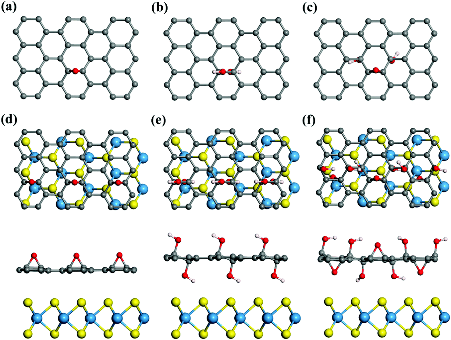 | ||
| Fig. 1 The building blocks of GO with (a) epoxy only, (b) hydroxyl only and (c) both epoxy and hydroxyl; (d–f) top view and side view of the GO structures with different oxygen functionalities. | ||
For the WS2 and e-GO hybrid, the C–O bond length is 1.47 Å, which is 0.03 Å larger than that in GO without WS2. The distance between them is similar to that of WS2/graphene. We have considered two types of e-GO structures, including epoxy distributed on only one side of graphene and both sides of graphene, and the structural stability of e-GO with WS2 to form the heterostructures are compared (the binding energies are shown in Fig. S2 of the ESI†). Thermodynamically, the heterostructures of WS2 and e-GO with epoxy located a on single side (Fig. 1d) is energetically favorable, so we chose this type of structure for further discussion. For WS2 and h2-GO, the hydroxyl functionals distribute on both sides of GO and induce a larger distance of 3.69 Å between WS2 and GO compared to that of 3.33 Å between WS2 and graphene. In addition, we investigated WS2 and GO with both hydroxyl and epoxy functionalities, and the ratio of epoxy and hydroxyl is 1![[thin space (1/6-em)]](https://www.rsc.org/images/entities/char_2009.gif) :2 (as shown in Fig. 1c). In this case, the distance between WS2 and GO is 3.67 Å, which is still larger than that between WS2 and graphene. The interaction between WS2 and GO with different oxygen concentrations is systematically investigated and plotted in Fig. 2a. The oxygen concentration is defined as the ratio of the number of sp3 C atoms to the total number of C atoms. Generally speaking, as the concentration of the oxygen groups increases, the binding energies between WS2 and GO gradually increase. In the case of WS2 and e-GO, the binding energies keep constant at about 0.19 eV per WS2 unit and starts to greatly increase from the oxygen concentration of 80%. When the GO is fully oxidized by only epoxy groups, the binding energy between GO and WS2 can reach 0.214 eV per WS2. It is different from the other two cases of h2-GO and h2e-GO. In these two cases, the binding energies continuously increases from low oxygen concentration, especially from the oxygen coverage of 40% due to the formation of a chain-like structure. Compared with these three cases, the e-GO possess the largest binding energies with WS2, especially at low oxygen concentration. For example, at the oxygen concentration of 16%, the binding energy per WS2 unit of e-GO is 0.187 eV, which is 0.06 eV and 0.07 eV larger than that of the h2e-GO and h2-GO motifs, respectively. The binding distances between C atoms from GO and the nearest S atoms from WS2 are 3.31 Å, 3.97 Å and 4.37 Å for e-GO, h2e-GO and h2-GO, respectively, at the oxygen concentration of 16%. We also calculated the variation of distances between GO and WS2 as a function of oxygen concentrations, which is plotted in Fig. S3 of the ESI.† Due to the larger buckling of the GO surface at high oxygen coverage, the distance between WS2 and GO is defined as the vertical distance between the nearest S atoms from WS2 and O atoms from GO. Our results show that the distances between GO (h2-GO and h2e-GO) and WS2 increase as the oxygen concentration increases.
:2 (as shown in Fig. 1c). In this case, the distance between WS2 and GO is 3.67 Å, which is still larger than that between WS2 and graphene. The interaction between WS2 and GO with different oxygen concentrations is systematically investigated and plotted in Fig. 2a. The oxygen concentration is defined as the ratio of the number of sp3 C atoms to the total number of C atoms. Generally speaking, as the concentration of the oxygen groups increases, the binding energies between WS2 and GO gradually increase. In the case of WS2 and e-GO, the binding energies keep constant at about 0.19 eV per WS2 unit and starts to greatly increase from the oxygen concentration of 80%. When the GO is fully oxidized by only epoxy groups, the binding energy between GO and WS2 can reach 0.214 eV per WS2. It is different from the other two cases of h2-GO and h2e-GO. In these two cases, the binding energies continuously increases from low oxygen concentration, especially from the oxygen coverage of 40% due to the formation of a chain-like structure. Compared with these three cases, the e-GO possess the largest binding energies with WS2, especially at low oxygen concentration. For example, at the oxygen concentration of 16%, the binding energy per WS2 unit of e-GO is 0.187 eV, which is 0.06 eV and 0.07 eV larger than that of the h2e-GO and h2-GO motifs, respectively. The binding distances between C atoms from GO and the nearest S atoms from WS2 are 3.31 Å, 3.97 Å and 4.37 Å for e-GO, h2e-GO and h2-GO, respectively, at the oxygen concentration of 16%. We also calculated the variation of distances between GO and WS2 as a function of oxygen concentrations, which is plotted in Fig. S3 of the ESI.† Due to the larger buckling of the GO surface at high oxygen coverage, the distance between WS2 and GO is defined as the vertical distance between the nearest S atoms from WS2 and O atoms from GO. Our results show that the distances between GO (h2-GO and h2e-GO) and WS2 increase as the oxygen concentration increases.
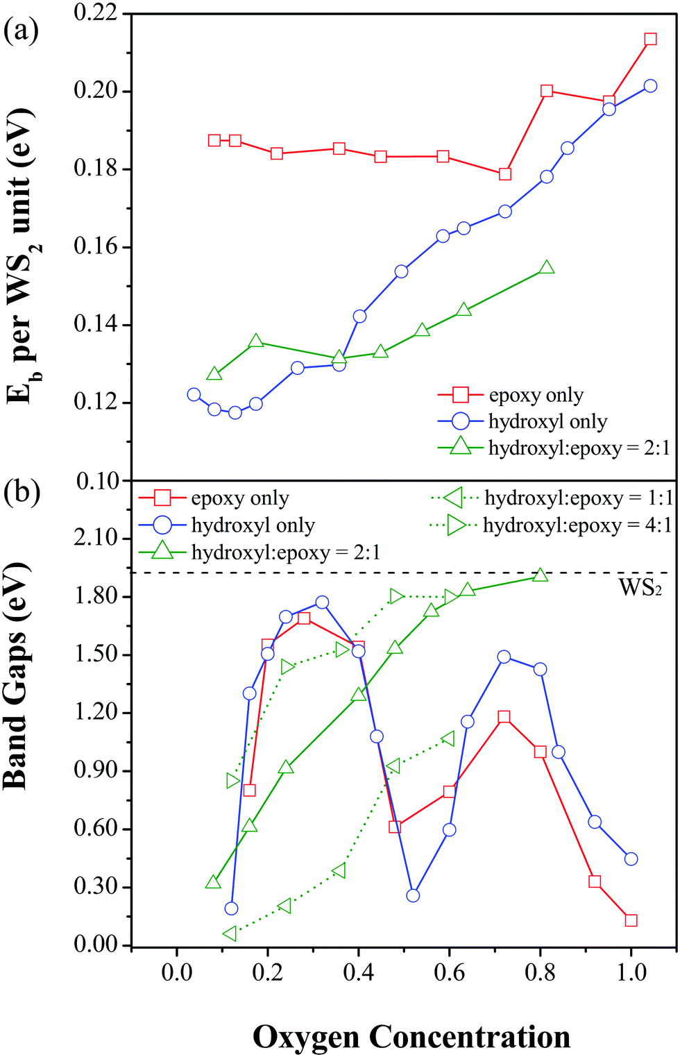 | ||
| Fig. 2 (a) Binding energies between WS2 and GO with different oxygen concentration; (b) variations of band gaps of the WS2/GO heterostructures as the oxygen concentration increases. | ||
On the basis of the stable WS2/GO structures, we further investigated the electronic properties that are induced by the different oxygen concentrations of GO. Previous theoretical studies reported that the band gaps of GO can be modulated by different surface oxidation.43–45 Thus, we propose the electronic properties of WS2/GO heterostructures can be efficiently controlled by changing the oxygen functionalities on the GO surface. The variation of band gaps of the WS2/GO heterostructures with different oxygen concentration are shown in Fig. 2b. For the case of WS2 with h2e-GO, the band gap increases linearly with increase in the oxygen concentration, and finally reaches the maximum value of 1.91 eV with an oxygen coverage of 80%, which is close to the band gap of pristine WS2. The band gaps of the pure h2e-GO structures without WS2 also go up as the oxygen concentration increases but all of them are greatly larger than that of h2e-GO with WS2 (see the Fig. S4 in the ESI†). For example, a higher band gap of 3.11 eV is obtained for pure h2e-GO at the oxygen coverage of 80%. Thus, electronic coupling between WS2 and GO is proven and influences the bond length of both WS2 and GO. For instance, take WS2 and h2e-GO heterostructure with the oxygen concentration of 80% as an example: the bond lengths of W–S and O–C are elongated by about 0.4% and 1.4%, respectively, in contrast to the free-standing ones. In order to make sure that the band gap variation is the general rule, more structural models have been taken into account. We have considered the other two types of GO models with hydroxyl to epoxy ratios of 1:1 and 4:1 (the structures can be seen in Fig. S5 in the ESI†). The band gaps are calculated and plotted by the dashed line in Fig. 2b. As it is shown, the trends of band gaps in both WS2/he-GO and WS2/h4e-GO heterostructures are similar to those of the WS2/h2e-GO structures, but only with different values. Importantly, we found that the band gaps of WS2/GO are dependent on the hydroxyl concentrations in GO, and GO with larger hydroxyl to epoxy ratio possesses larger band gaps, such as GO with a hydroxyl to epoxy ratio of 4:1. For example, at the same oxygen concentration of 48%, the band gaps of he-GO, h2e-GO and h4e-GO with WS2 are 0.93 eV, 1.53 eV and 1.80 eV, respectively. Different from the WS2 on GO with both hydroxyl and epoxy, the band gaps of both WS2 with h2-GO and e-GO exhibit an “M” shape as the oxygen concentration increases. Two peaks in the “M” shape correspond to the formation of chain-like structures, and their structures are shown in Fig. S4 of the ESI.† For the WS2 and e-GO, the band gaps on the two peaks are 1.69 eV and 1.18 eV at the oxygen concentration of 28% and 72%, respectively, which are slightly smaller than those of the WS2 and h2-GO (1.77 eV and 1.49 eV at the oxygen concentration of 32% and 72%). The peak valley of the band gaps is present with the oxygen concentration at about 50%, corresponding to incomplete-chain GO structures (see the Fig. S5 in the ESI†). We also examined the electronic properties of the pure GO structures and made a comparison, which is shown in Fig. S4 in the ESI.† We find that the tendency of the band gaps of WS2 on h2-GO or e-GO is similar to that of GO without WS2 at low oxygen concentration, but is different when the oxygen concentration is beyond 70% due to the relatively stronger interaction between WS2 and GO at high oxygen concentration. Therefore, to a certain extent, the electronic properties of WS2 and GO hybrids are dependent on the atomic structures and oxygen concentrations of GO. Due to tungsten being a heavy element, we also considered the calculations with spin–orbit coupling (SOC) effect and compared with the results without SOC effect (see Table S1, ESI†). The band gaps of WS2 and GO heterostructures calculated using the PBE functional with SOC effect are all smaller than those without considering SOC effect, but the difference is very small. For example, the band gap of WS2/h2e-GO with oxygen concentration of 40% is 1.15 eV with PBE plus SOC effect, slightly smaller than 1.29 eV without considering SOC effect.
To further understand the electronic properties of WS2/GO heterostructures, the band structures and the partial charge density distributions for pristine WS2 and WS2/GO hybrids are plotted in Fig. 3. Monolayer WS2 is a semiconductor with a direct band gap at the K point, which is consistent with previous studies.46,47 From the partial charge density distribution, the conduction band minimum (CBM) and valence band maximum (VBM) of WS2 are both dominated by d-orbital states of W atoms in a ligand field. For WS2/GO heterostructures, the band structures vary for different oxygen functionalities and concentrations. They are either indirect or direct semiconductors, which depend on the energy band structures of GO. For example, as shown in Fig. 3, when the oxygen concentration is 40%, WS2 on h2-GO and e-GO are semiconductors with direct band gaps of 1.52 eV and 1.54 eV, respectively. We also observed that the CBM and VBM are separated and distributed on different layers (see the inset figures in Fig. 3). In the case of WS2 and h2e-GO with an oxygen coverage beyond 40%, the CBM is distributed on GO while the VBM is located on WS2. But, it is different from the cases of WS2 on both h2-GO and e-GO surfaces. In these two cases, both CBM and VBM distribute on GO at an oxygen concentration smaller than 80%, and beyond 80%, the CBM and VBM for the WS2/GO structures are spatially separated and distributed on WS2 and GO, respectively.
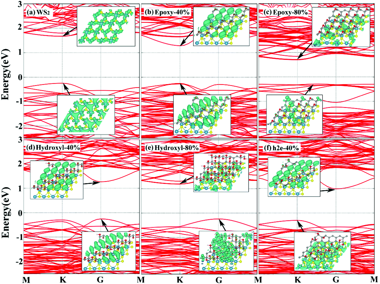 | ||
| Fig. 3 Band structures of (a) monolayer WS2 and (b–f) WS2/GO heterostructures. The inset figure shows the partial charge density at the CBM and VBM. | ||
Work function (WF), which represents the energy difference between the vacuum energy level and the Fermi energy level, is an important factor for materials to be used in electronic devices.48–50 The vacuum energy level is defined as the averaged effective potential across the plane that is parallel to the heterostructure, and 12 Å away from the nearest atomic layers of the heterostructure in the supercell. Our calculated work function for monolayer WS2 is 5.65 eV, which agrees well with the previous theoretical result of 5.89 eV.51 The calculated work functions for WS2 and GO with different oxygen functionalities and concentrations are summarized and plotted in Fig. 4. Obviously, the WF of WS2/GO hybrids can be efficiently modulated by the surface oxidation of GO and the WF tendencies are similar to those of the band gaps. For WS2 and h2e-GO hybrids, the WF gradually goes up from 4.78 eV to 5.55 eV, finally close to the WF of WS2. In order to make sure that the work function variation is the general rule, we have also calculated the other two types of GO models with hydroxyl to epoxy ratios of 1:1 and 4:1. As is shown in Fig. 4, the work functions for WS2/he-GO and WS2/h4e-GO heterostructures are almost the same as those of the WS2/h2e-GO structures. The WF variations of both WS2/e-GO and WS2/h2-GO show the “M” shape as the band gaps. It is worth noting that the WF of WS2/e-GO hybrids becomes larger than that of pure WS2 when the oxygen concentration is beyond 20%, while the WF of WS2/h2-GO hybrids are all smaller compared to that of pure WS2 at the whole range of oxygen concentrations. The lowest WF value of 4.09 eV occurs in WS2/h2-GO which fully oxidized with hydroxyl groups, and the largest WF values reach 6.34 eV at the WS2/e-GO with the only epoxy concentration at 80%. The tunable WF values modulated by GO with different oxidations can efficiently modulate the carrier concentration of WS2, and there is the possibility to further modulate the carrier mobility by filling in the traps in WS2 with abundant carriers. This promotes WS2 and other TMD materials as promising electronic devices.
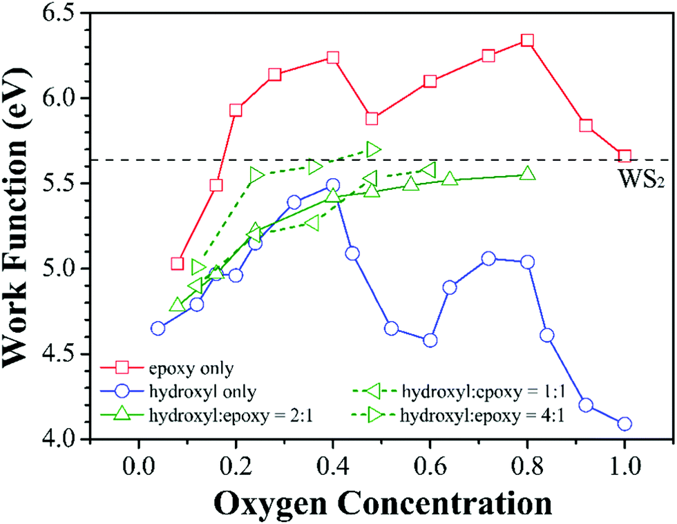 | ||
| Fig. 4 Variations of work function of WS2/GO heterostructures as the oxygen concentration increases. | ||
Conclusions
In summary, we investigated the structures and electronic properties of WS2 and GO heterostructures using first-principles calculations, and the interlayer binding energies, band structures and work functions of WS2 and GO with various oxygen functionalities and concentrations have been obtained. The energies are not sensitive to different WS2/GO stacking configurations, and we chose the H configuration for the calculations. We considered three conditions for the GO structures: only epoxy (e-GO), only hydroxyl (h2-GO) and both epoxy and hydroxyl (he-GO, h2e-GO and h4e-GO) on the graphene surface. As the concentration of the oxygen groups increases, the binding energies between WS2 and GO gradually increase, and e-GO possess the largest binding energies with WS2 compared to the other GO structures. The band gaps of the WS2/GO hybrids can be efficiently modulated in a wide range from 0.13 eV to 1.91 eV, which are dependent on the atomic structures and oxygen concentrations of GO. Based on the analysis of the band structures and the partial charge density distributions, the separated CBM and VBM for the WS2/GO hybrids are observed, and they are distributed on different layers at certain oxygen concentrations. In addition, we also calculate the work functions of different WS2/GO heterostructures, which possess the similar tendency of the band gaps. The lowest WF value of 4.09 eV occurs at the WS2 and GO fully oxidized by hydroxyl groups, while the largest WF values can reach 6.34 eV for the WS2 and GO with the only epoxy concentration at 80%. Our theoretical results provide an effective way to modulate the electronic properties of 2D TMD nanomaterials and make them ideal for high-performance electronic devices.Acknowledgements
We acknowledge the support from the National Natural Science Foundation of China (Grant No. 21403146, 21273158, 21673149), Natural Science Foundation of Jiangsu Province (Grant No. BK20140314), a Project Funded by the Priority Academic Program Development of Jiangsu Higher Education Institutions (PAPD). This is also a project supported by the Fund for Innovative Research Teams of Jiangsu Higher Education Institutions, Jiangsu Key Laboratory for Carbon-Based Functional Materials and Devices, and the Collaborative Innovation Center of Suzhou Nano Science and Technology.References
- M. Kin Fai, H. Keliang, L. Changgu, L. Gwan Hyoung, H. James, T. F. Heinz and S. Jie, Nat. Mater., 2012, 12, 207–211 CrossRef PubMed.
- X. Duan, C. Wang, A. Pan, R. Yu and X. Duan, Chem. Soc. Rev., 2015, 44, 8859–8876 RSC.
- D. Jariwala, V. K. Sangwan, L. J. Lauhon, T. J. Marks and M. C. Hersam, ACS Nano, 2014, 8, 1102–1120 CrossRef CAS PubMed.
- B. Radisavljevic, M. B. Whitwick and A. Kis, ACS Nano, 2011, 5, 9934–9938 CrossRef CAS PubMed.
- J. Pu, Y. Yomogida, K. K. Liu, L. J. Li, Y. Iwasa and T. Takenobu, Nano Lett., 2012, 12, 4013–4017 CrossRef CAS PubMed.
- A. K. Singh, K. Mathew, H. L. Zhuang and R. G. Hennig, J. Phys. Chem. Lett., 2015, 6, 1087–1098 CrossRef CAS PubMed.
- Y. Jing, Z. Zhou, C. R. Cabrera and Z. Chen, J. Phys. Chem. C, 2013, 117, 25409–25413 CAS.
- L. Yang, K. Majumdar, H. Liu, Y. Du, H. Wu, M. Hatzistergos, P. Y. Hung, R. Tieckelmann, W. Tsai, C. Hobbs and P. D. Ye, Nano Lett., 2014, 14, 6275–6280 CrossRef CAS PubMed.
- K. He, C. Poole, K. F. Mak and J. Shan, Nano Lett., 2013, 13, 2931–2936 CrossRef CAS PubMed.
- N. Lu, H. Guo, L. Li, J. Dai, L. Wang, W. N. Mei, X. Wu and X. C. Zeng, Nanoscale, 2014, 6, 2879–2886 RSC.
- H. Pan, J. Phys. Chem. C, 2014, 118, 13248–13253 CAS.
- H. Zhang, L.-M. Liu and W.-M. Lau, J. Mater. Chem. A, 2013, 1, 10821 CAS.
- W. J. Yu, Z. Li, H. Zhou, Y. Chen, Y. Wang, Y. Huang and X. Duan, Nat. Mater., 2013, 12, 246–252 CrossRef CAS PubMed.
- H. L. Zhuang and R. G. Hennig, J. Phys. Chem. C, 2013, 117, 20440–20445 CAS.
- D. Braga, I. Gutierrez Lezama, H. Berger and A. F. Morpurgo, Nano Lett., 2012, 12, 5218–5223 CrossRef CAS PubMed.
- K. K. Kam and B. A. Parkinson, J. Phys. Chem., 1982, 86, 463–467 CrossRef CAS.
- S. Jo, N. Ubrig, H. Berger, A. B. Kuzmenko and A. F. Morpurgo, Nano Lett., 2014, 14, 2019–2025 CrossRef CAS PubMed.
- X. H. Wang, J. Q. Ning, Z. C. Su, C. C. Zheng, B. R. Zhu, L. Xie, H. S. Wu and S. J. Xu, RSC Adv., 2016, 6, 27677–27681 RSC.
- A. K. Geim and I. V. Grigorieva, Nature, 2013, 499, 419–425 CrossRef CAS PubMed.
- X. Duan, C. Wang, J. C. Shaw, R. Cheng, Y. Chen, H. Li, X. Wu, Y. Tang, Q. Zhang and A. Pan, Nat. Nanotechnol., 2014, 9, 1024–1030 CrossRef CAS PubMed.
- S. Tongay, W. Fan, J. Kang, J. Park, U. Koldemir, J. Suh, D. S. Narang, K. Liu, J. Ji, J. Li, R. Sinclair and J. Wu, Nano Lett., 2014, 14, 3185–3190 CrossRef CAS PubMed.
- Y. Gong, J. Lin, X. Wang, G. Shi, S. Lei, Z. Lin, X. Zou, G. Ye, R. Vajtai and B. I. Yakobson, Nat. Mater., 2014, 13, 1135–1142 CrossRef CAS PubMed.
- Y. Li, H. Wang, L. Xie, Y. Liang, G. Hong and H. Dai, J. Am. Chem. Soc., 2011, 133, 7296–7299 CrossRef CAS PubMed.
- H. Li, K. Yu, C. Li, Z. Tang, B. Guo, X. Lei, H. Fu and Z. Zhu, Sci. Rep., 2015, 5, 18730 CrossRef CAS PubMed.
- J. Zhang, Q. Wang, L. Wang, X. Li and W. Huang, Nanoscale, 2015, 7, 10391–10397 RSC.
- Z. Wang, T. Chen, W. Chen, K. Chang, L. Ma, G. Huang, D. Chen and J. Y. Lee, J. Mater. Chem. A, 2013, 1, 2202–2210 CAS.
- Y. Liu, J. Mater. Chem. A, 2014, 2, 13109–13115 CAS.
- X. Xie, Z. Ao, D. Su, J. Zhang and G. Wang, Adv. Funct. Mater., 2015, 25, 1393–1403 CrossRef CAS.
- S. Ratha and C. S. Rout, ACS Appl. Mater. Interfaces, 2013, 5, 11427–11433 CAS.
- J. Yang, D. Voiry, S. J. Ahn, D. Kang, A. Y. Kim, M. Chhowalla and H. S. Shin, Angew. Chem., Int. Ed., 2013, 52, 13751–13754 CrossRef CAS PubMed.
- Y. Ma, Y. Dai, M. Guo, C. Niu and B. Huang, Nanoscale, 2011, 3, 3883–3887 RSC.
- R. Sharma, J. Aneesh, R. K. Yadav, S. Sanda, A. R. Barik, A. K. Mishra, T. K. Maji, D. Karmakar and K. V. Adarsh, Phys. Rev. B: Condens. Matter Mater. Phys., 2016, 93, 155433 CrossRef.
- S. S. Li, C. W. Zhang and W. X. Ji, Mater. Chem. Phys., 2015, 164, 150–156 CrossRef CAS.
- T. Musso, P. V. Kumar, A. S. Foster and J. C. Grossman, ACS Nano, 2014, 8, 11432–11439 CrossRef CAS PubMed.
- G. Kresse and J. Furthmüller, Phys. Rev. B: Condens. Matter Mater. Phys., 1996, 54, 11169–11186 CrossRef CAS.
- G. Kresse and J. Furthmüller, Comput. Mater. Sci., 1996, 6, 15–50 CrossRef CAS.
- J. P. Perdew, K. Burke and M. Ernzerhof, Phys. Rev. Lett., 1996, 77, 3865–3868 CrossRef CAS PubMed.
- M. Dion, H. Rydberg, E. Schroder, D. C. Langreth and B. I. Lundqvist, Phys. Rev. Lett., 2004, 92, 246401 CrossRef CAS PubMed.
- Y. Ma, Y. Dai, W. Wei, C. Niu, L. Yu and B. Huang, J. Phys. Chem. C, 2011, 115, 20237–20241 CAS.
- S. S. Li and C. W. Zhang, J. Appl. Phys., 2013, 114, 183709 CrossRef.
- L. Wang, Y. Y. Sun, K. Lee, D. West, Z. F. Chen, J. J. Zhao and S. B. Zhang, Phys. Rev. B: Condens. Matter Mater. Phys., 2010, 82, 161406 CrossRef.
- J. Yan and M. Y. Chou, Phys. Rev. B: Condens. Matter Mater. Phys., 2015, 82, 1303–1307 Search PubMed.
- T.-F. Yeh, J.-M. Syu, C. Cheng, T.-H. Chang and H. Teng, Adv. Funct. Mater., 2010, 20, 2255–2262 CrossRef CAS.
- J. A. Yan, L. Xian and M. Y. Chou, Phys. Rev. Lett., 2009, 103, 086802 CrossRef PubMed.
- J. Ito, J. Nakamura and A. Natori, J. Appl. Phys., 2008, 103, 113712 CrossRef.
- T. Georgiou, R. Jalil, B. D. Belle, L. Britnell, R. V. Gorbachev, S. V. Morozov, Y. J. Kim, A. Gholinia, S. J. Haigh and O. Makarovsky, Nat. Nanotechnol., 2013, 8, 100–103 CrossRef CAS PubMed.
- S. Ratha, A. J. Simbeck, D. J. Late, S. K. Nayak and C. S. Rout, Appl. Phys. Lett., 2014, 105, 243502 CrossRef.
- R. C. Shallcross, T. Stubhan, E. L. Ratcliff, A. Kahn, C. J. Brabec and N. R. Armstrong, J. Phys. Chem. Lett., 2015, 6, 1303–1309 CrossRef CAS PubMed.
- P. Wang, D. Tanaka, S. Ryuzaki, S. Araki, K. Okamoto and K. Tamada, Appl. Phys. Lett., 2015, 107, 151601 CrossRef.
- M. Zhou, R. Q. Png, S. H. Khong, S. Sivaramakrishnan, L. H. Zhao, L. L. Chua, R. H. Friend and P. K. H. Ho, Appl. Phys. Lett., 2012, 101, 1–7 Search PubMed.
- N. A. Lanzillo, A. J. Simbeck and S. K. Nayak, J. Phys.: Condens. Matter, 2015, 27, 175501 CrossRef PubMed.
Footnote |
| † Electronic supplementary information (ESI) available. See DOI: 10.1039/c6tc04487e |
| This journal is © The Royal Society of Chemistry 2017 |