
Composition-tunable 2D SnSe2(1−x)S2x alloys towards efficient bandgap engineering and high performance (opto)electronics†
Yan
Wang
a,
Le Huang
a,
Bo
Li
a,
Jimin
Shang
a,
Congxin
Xia
b,
Chao
Fan
c,
Hui-Xiong
Deng
a,
Zhongming
Wei
*a and
Jingbo
Li
*a
aState Key Laboratory for Superlattices and Microstructures, Institute of Semiconductors, University of Chinese Academy of Sciences, Chinese Academy of Sciences, Beijing 100083, China. E-mail: zmwei@semi.ac.cn; jbli@semi.ac.cn
bDepartment of Physics, Henan Normal University, Xinxiang 453007, China
cSchool of Electronics and Information Engineering, Hebei University of Technology, Tianjin 300401, China
First published on 17th November 2016
Abstract
Efficient bandgap engineering is a significant strategy for the utilization of widely concerned two-dimensional (2D) layered materials in versatile devices such as nanoelectronics, optoelectronics, and photonics. Alloying transition-metal dichalcogenides (TMDs) with different components has been proved as a very effective way to get 2D nanostructured semiconductors with artificially designed tunable bandgaps. Here we report a systematically study of chemical vapor transport (CVT) grown SnSe2(1−x)S2x alloys with continuously bandgaps ranging from 1.37 eV (SnSe2) to 2.27 eV (SnS2). The carrier mobility of 2D SnSe2(1−x)S2x nanosheets can be tuned from 2.34 cm2 V−1 s−1 (SnS2) to 71.30 cm2 V−1 s−1 (SnSe2) by controlling the S composition in the alloy. Furthermore, the carrier mobility of SnSeS increase from 10.34 to 12.16 cm2 V−1 s−1 under illumination, showing excellent optoelectronic properties. Our study suggests that SnSe2(1−x)S2x nanosheets is a highly qualified 2D materials for next-generation nanoelectronics and optoelectronics application.
1. Introduction
Since the discovery of graphene,1,2 two-dimensional (2D) layered materials such as transition-metal dichalcogenides (TMDs), have attracted considerable attention for their unique electronic properties and potential applications.3–6 The atomic layers of TMDs are weakly bonded together by van der Waals interactions and can be isolated into single- or few-layer nanosheets. Unlike graphene with a zero bandgap, TMDs possess sizable bandgaps, which is essential for digital electronics and optoelectronics applications.7 Bandgap engineering is favourable to providing great flexibility in designing optoelectronic devices of TMDs.8 Alloying TMDs has been proven as a very effective way to realize the bandgap engineering.9–11 A series of 2D-TMDs alloy nanosheets with tunable bandgaps, such as Mo1−xWxS2,12,13 WS2(1−x)Se2x,8,14 MoS2(1−x)Se2x,15–24 Mo1−xWxSe2,25 have shown different optical and electrical properties.Recently, tin dichalcogenides (SnS2, SnSe2)26–33 have driven considerable attention on their high carrier mobility and excellent photoresponsive property. Furthermore, the properties of environmental friendly, earth abundant and low-cost make tin dichalcogenides desirable for sustainable optoelectronic devices. SnS2 and SnSe2 are layered materials with a hexagonal CdI2 type crystal structure and exhibits indirect bandgap. Due to the big difference of bandgaps between SnS2 and SnSe2 (the bandgaps of SnS2 and SnSe2 is about 2.1 eV and 1.0 eV, respectively), theoretically, alloying SnS2 and SnSe2 can be valid for bandgap engineering.34 In addition to the widely tunable bandgaps, based on previously reports, SnSe2(1−x)S2x alloys may also possess tunable carrier mobility35 with the variation of S composition due to the significantly different carrier mobility between SnSe232 and SnS2.29 All these tunable properties of SnSe2(1−x)S2x alloys are beneficial for developing versatile devices.36–38
In this work, a systematically study of 2D SnSe2(1−x)S2x alloys have been performed. The bulk SnSe2(1−x)S2x crystals with five different S compositions (x = 0, 0.25, 0.5, 0.75 and 1, respectively) have been alloyed by chemical vapor transport (CVT) method. 2D few and monolayer SnSe2(1−x)S2x nanosheets are then fabricated by mechanically exfoliated method. Energy Dispersive X-ray Spectrom (EDX) mapping and high resolution transmission electron microscopy (HRTEM) imaging reveal a random arrangement of the S and Se atoms in the 2D alloys. The UV-visible absorption spectra shows a continuously tunable bandgaps of SnSe2(1−x)S2x from 1.37 eV to 2.27 eV, which is in accordance with our DFT calculation result. Field-effect transistors (FETs) fabricated on few-layer SnSe2(1−x)S2x nanosheets show obvious modulation of carrier mobility with variation of S composition from 2.34 cm2 V−1 s−1 (SnS2) to 71.30 cm2 V−1 s−1 (SnSe2). The SnSe2(1−x)S2x nanosheets also possess good photo responsive property. The carrier mobility of SnSeS FET increase from 10.34 to 12.16 cm2 V−1 s−1 under illumination (532 nm laser, 514.6 mW cm−2 of the power), indicating that SnSe2(1−x)S2x nanosheets have the potential application in phototransistors.
2. Experimental methods
2.1. The growth of SnSe2(1−x)S2x alloy crystals
Bulk SnSe2(1−x)S2x crystals are grown by chemical vapor transport (CVT) reaction technique with iodine as the transport agent, as reported in previous work.39 Vacuum evacuated ampoules loaded with reactants are maintained in one-zone furnace for 72 h with the ampoules placed at the hot-zone (T = 650 °C) of the furnace enabling SnSe2(1−x)S2x alloy crystals to be transported and grown in the cooler end. Then the furnace is air-cooled to room temperature and the SnSe2(1−x)S2x crystals are prepared.2.2. Fabrication of the transistors
The transistors based on SnSe2(1−x)S2x nanosheets are all fabricated with “PPT (Photolithography patterning and transferring)” technique as described in previous work.40 A clean SiO2/Si wafer is firstly coated with photo resist and covered by Lithography mask then exposed under straight halogen lamp light for 30 min in order to etch patterning electrodes. Thereafter, the SiO2/Si wafer is immersed in the 0.8% Tetramethylammonium hydroxide (TMAH) water solution for 25 s to remove the photo resist in exposure region. Subsequently, the wafer is covered by 60 nm Au through evaporation, and then immersed in acetone for removing redundant Au layer and photo resist, leaving the Au-electrode arrays on the substrate. For fabricating the single nanosheets transistors, the prepared Au-electrode arrays are then transferred with a PMMA transfer method41 onto specific SnSe2(1−x)S2x nanosheets samples which have been prepared in advanced with micromechanical exfoliation technique on 300 nm SiO2/Si substrate. After dissolved PMMA film with acetone, SnSe2(1−x)S2x transistors are prepared and then annealed at 300 °C for 30 min.2.3. Measurements and characterization
Raman spectra are obtained by Renishaw in Wia plus under a 514 nm laser. TEM, HRTEM image and EDX mapping are conducted on an FEI/Tecnai G2 F20 S-TWIN TMP. All the electrical measurements are performed with a transistor test system (Agilent-B2902). The optical absorption properties of all samples are measured with UV-vis spectroscopy (Varian, Cray 5E).3. Results and discussion
Fig. 1a presents an optical image of exfoliated SnSe0.5S1.5 flakes with monolayer region. The inset in Fig. 1a is a photograph of SnSe0.5S1.5 single crystal. The atomic force microscopy (AFM) image of this alloy sheet is shown in Fig. 1b, with an inset showing a height of about 1.2 nm for the monolayer. This height of monolayer is larger than the theoretical interlayer distance in SnSe0.5S1.5 bulk materials (∼0.7 nm), which can be attributed to the instrumental offset (∼0.5 nm) phenomenon that is commonly observed in AFM imaging of TMDs monolayers.42 Raman spectra are used to characterize the composition dependent vibration modes of all the synthesized SnSe2(1−x)S2x alloy crystals. Fig. 1c shows Raman (310–315 cm−1) mapping image of the same SnSe0.5S1.5 sample with Fig. 1b. As shown in Fig. 1c, the false color brightness of monolayer SnSe0.5S1.5 sample is much weaker than few-layer samples adjacent to it. Since increasing false color brightness of Raman mapping indicates increasing Raman signal, the Raman signal of monolayer SnSe0.5S1.5 sample is much weaker than few-layer ones. Fig. 1d presents the normalized Raman spectra of as-prepared SnSe2(1−x)S2x samples with composition x decreased gradually from 1 (top, pure SnS2) to 0 (bottom, pure SnSe2). Pure SnS2 exhibit an intense peak at 313 cm−1, corresponding to A1g(S–Sn) mode reported by previous work.43,44 The absence of Eg mode at 210 cm−1 probably results from the reduction of scattering centers for Eg mode when the thickness of SnS2 decreased down to nanometer scale, as shown in Fig. S1 (ESI†). By contrast, for SnSe2 sample, A1g(Se–Sn) mode at 181 cm−1 and Eg(Se–Sn) mode at 109 cm−1 are observed.44 With the decrement of S composition, A1g(S-Sn) mode gradually decrease until it disappear completely, while A1g(Se-Sn) and Eg(Se-Sn) gradually come into appearance with increment of Se composition. As shown in Fig. 1d, the full width at half maxium (FWHM) of SnSe2-like A1g mode increases from 5.64 cm−1 (x = 0) to 24.15 cm−1 (x = 0.5) and then decreases. SnSe2-like Eg mode and SnS2-like A1g mode also shows similar tendency with SnSe2-like A1g mode. Furthermore, the line shape of pure SnS2 and SnSe2 are symmetrical, while other SnSe2(1−x)S2x alloys (x = 0.75, 0.5 and 0.25) are asymmetrical. These asymmetric line shapes and peak broadening can both be attributed by the random S and Se distribution in SnSe2(1−x)S2x alloys. Due to the random distribution of S and Se, Sn atoms should have several different nearest S and Se coordination configurations in SnSe2(1−x)S2x alloys. This can result in the fluctuation of reduced mass and force constant, and thus cause the peak broadening and asymmetric line shapes of SnSe2(1−x)S2x alloys. The observed blue shift with increasing Se composition of SnS2-like Raman peak in Fig. 1d can be attributed by the lattice constants enlargement with the increment of Se composition. As shown in Fig. S4 (ESI†), as the lattice constants increase from 3.70 Å (SnS2) to 3.87 Å (SnSe2) with increasing Se composition, the SnS2-like A1g mode shows blue shift. Similarly, the red shift of SnSe2-like A1g and Eg modes with increasing S composition can also be attributed by the variation of lattice constants.13,45–47 This Raman shifts of the alloys also further confirm the expected compositional evolution in the SnSe2(1−x)S2x alloy nanosheets.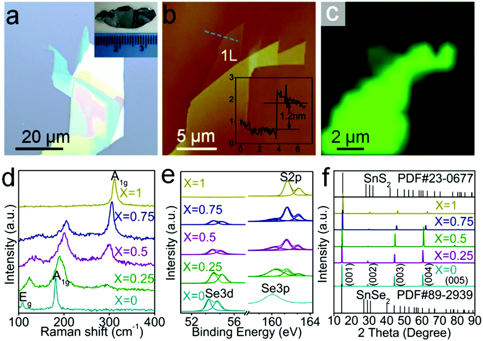 | ||
| Fig. 1 (a) Optical and (b) AFM image of SnSe0.5S1.5 nanosheets. Inset in panel (a) is a photograph of SnSe0.5S1.5 single crystal and inset in panel (b) is the height profile along the blue dotted line in (b), the thickness measured by AFM is about 1.2 nm, larger than the theoretical interlayer distance in SnSe0.5S1.5 bulk materials (∼0.7 nm), which can be attributed to the instrumental offset. (c) Raman (310–315 cm−1) mapping image of the same SnSe0.5S1.5 sample. (d) Raman spectra, (e) XPS, and (f) single crystal XRD pattern of bulk SnSe2(1−x)S2x samples. | ||
Fig. 1e plots X-ray photo-electron spectra (XPS) of all the synthesized SnSe2(1−x)S2x alloy crystals. The S compositions obtained through quantitative analysis of Se 3d and S 2p peaks are presented in Table S1 (ESI†), and the Sn 3d spectra of all SnSe2(1−x)S2x samples are shown in Fig. S2 (ESI†). These S compositions of the alloys are almost in accordance with the ratio of S in alloys predecessor, consistent with previously reported results.39
Fig. 1f shows the single crystal X-ray diffraction (XRD) patterns of five different crystals. The top of Fig. 1f shows that our SnS2 sample can be indexed with hexagonal unit cells of the CdI2-type (PDF#23-0677), while the bottom of Fig. 1f indicates the that the lattice of our SnSe2 sample is consistent with hexagonal SnSe2 (PDF#89-2939) What's more, all of the peaks are derived from the direction of c-axis, strongly suggesting its single crystalline nature. For each sample, the peaks corresponds to (001), (002), (003), (004), and (005) from left to right. Based on 2θ value of the (001) peak and λ of Cu Kα (λ = 1.5406 Å), the value of the (001) peak dspacing can be easily calculated through Bragg equation:
2dspacing![[thin space (1/6-em)]](https://www.rsc.org/images/entities/char_2009.gif) sinθ = λ sinθ = λ |
Transmission electron microscopy (TEM) with energy dispersive X-ray detector (EDX) capability is used for mapping element distribution in nanometer scales. Fig. 2a shows a typical TEM image of SnSeS few layers. EDX spectroscopy (Fig. 2b) shows well-resolved Sn, Se and S peaks, and the S content from EDX elemental analysis is x = 0.513, which almost consistent with the nominal one. The EDX mapping demonstrates a uniform distribution of Sn, Se and S in the sample (Fig. 2c–e).
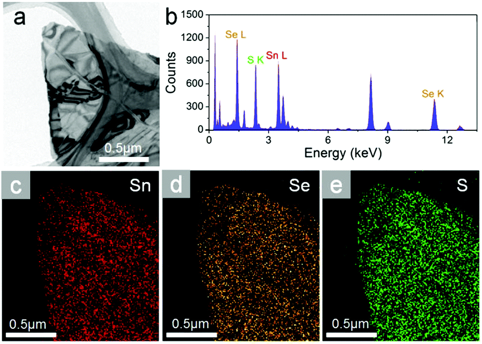 | ||
| Fig. 2 (a) Typical TEM image and (b) the corresponding EDX spectrum of SnSeS nanoflake. (c) Sn, (d) Se, and (e) S element mapping image for the same sheet. | ||
Fig. 3a shows the selected area electron diffraction (SAED) pattern taken from SnSeS nanosheet in Fig. 2a. The SAED pattern shows the lattice arrangement, further demonstrating the single crystral nature without significant defects of our as grown crystal.
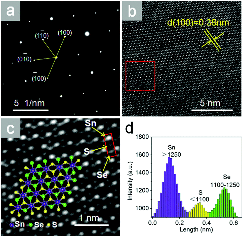 | ||
| Fig. 3 (a) The SAED pattern and (b and c) its HRTEM image taken from Fig. 2a. The red square in b outlines the part of the image shown in c. The hexagons consist of Sn, Se and S atoms as shown in the schematic illustration in the inset. Three spots with obviously different brightness in the red square of c represent the location of Sn, S, Se atoms. (d) The intensity profile shows the brightness of atoms in the red square in c from the top down. | ||
Fig. 3b exhibits the corresponding HRTEM image of the nanosheet, demonstrating the hexagonal structured lattice of SnSeS. The obtained lattice plane spacing from Fig. 3b is about 0.38 nm, which matches very well with the theoretical calculated (100) plane spacing value of 0.378 nm (Fig. S4, ESI†).
The HRTEM image can also been used to identify the distribution of the Se and S atoms in the SnSeS nanosheet as shown in Fig. 3c. HRTEM shows the Z-contrast (Z = atomic number) as images with atomic lateral resolution, as observed in Fig. 3c (see also the Fig. S3, ESI†). There are three levels of brightness in Fig. 3c. The intensity histograms of representative atoms with different brightness in the red square are shown in Fig. 3d. The homogeneous and brightest spots with intensity of >1250 arbitrary units (a.u.) represent Sn atoms, due to the Z number of Sn(50) is larger than those of S(16) and Se(34). Similarly, the medium-brightness spots with intensity of 1110–1250 a.u. represent Se atoms, and the dimmest spots with intensity of <1110 a.u. represent S atoms.
For clarity, some of the atoms can be denoted by purple, green and yellow spheres representing Sn, Se and S, respectively, thus a structural schematic can be drawn as the schematic illustration inset of Fig. 3c shown. As shown in the schematic illustration, it is clearly that the Se and S atoms are randomly distributed even in a single crystal lattice.
Fig. 4a presents the UV-vis absorption spectra and corresponding Tauc's plot (inset) of SnSe2(1−x)S2x with different S contents. Obvious blue shift behavior of the absorption edge is observed upon increasing the S content, suggesting that bandgaps are tuned with variation of S composition. Based on Tauc equation for indirect bandgap semiconductor:
| (αhν)1/2 = K(hν − Eg) |
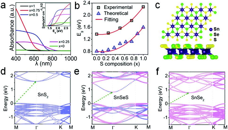 | ||
| Fig. 4 (a) UV-vis absorption spectra of different SnSe2(1−x)S2x bulk samples, inset is Tauc's plot of corresponding samples. (b) The statistical analysis of the bandgap modulation in the as-grown bulk SnSe2(1−x)S2x. The observed tuning of the bandgap in the SnSe2(1−x)S2x (blue spots) is consistent with our theoretical calculations (black spots) and bowing equation fitting curve (two red lines). (c) Top view and side view of models of SnSeS. (d–f) Calculated projected band structure of the different SnSe2(1−x)S2x (x = 0, 0.5 and 1) alloys. The blue and pink dots in the figures denote the bands dominated by SnS2 and SnSe2, respectively. | ||
| x value in SnSe2(1−x)S2x predecessor | UV-vis absorption | |
|---|---|---|
| Absorption edge λ (nm) | E g (eV) | |
| 1 | 545 | 2.27 |
| 0.75 | 680 | 1.82 |
| 0.5s | 790 | 1.57 |
| 0.25 | 880 | 1.41 |
| 0 | 905 | 1.37 |
To understand the composition-dependent electronic structure of SnSe2(1−x)S2x alloys, DFT calculations are conducted for their monolayers. The optimized lattice constants of monolayer SnS2 and SnSe2 are α1 = 3.70 Å and α2 = 3.89 Å, consistent with previous results.34 Since a ‘random’ behaviour of the SnSe2(1−x)S2x alloy has been verified,34 super cells consisting of a 4 × 4 unit cells are constructed with random distribution of S and Se atoms at chalcogenide atom sites and more composition values are used (a configuration for SnSeS shown in Fig. 4c).
All the SnSe2(1−x)S2x alloys are optimized with relaxing their lattice constants (further details see ESI†). Evolution of the lattice constant of SnSe2(1−x)S2x alloy with S concentration is shown in Fig. S4 (ESI†). A nearly linear variation is revealed, indicating the Vegard's law.
Fig. 4d–f and Fig. S5 (ESI†) illustrates the band structures of SnSe2(1−x)S2x alloys with different S composition. The blue and pink dots in the Figures denote the bands dominated by SnS2 and SnSe2, respectively. As can be seen, single-layer SnS2 and SnSe2 exhibit indirect bandgaps of 1.60 eV and 0.81 eV, respectively. Both are smaller than the experimental results due to the underestimation of GGA-PBE functional. It is indicated that monolayer SnSe2(1−x)S2x exhibits the modulation of its bandgap by the S content. Interestingly, SnSe2(1−x)S2x with a small S content obtains a narrower rather than wider bandgap. Generally, the bandgap increases with the S concentration. Further insight can be obtained from the variation of the bandgap with the S content, as shown in Fig. 4b (black spots). The bandgap does not show linear variation with the S concentration, indicating the band bowing effect. Fitting to the conventional bowing equation (Fig. 4b, red lines)
| Eg(x) = xEg(SnS2) + (1 − x)Eg(SnSe2) − bx(1 − x) |
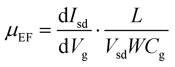
To probe the electrical properties of the SnSe2(1−x)S2x alloys, SnSe2(1−x)S2x few layers field-effect transistors (FETs) are also fabricated and measured, as shown in Fig. 5 and Fig. S6 (ESI†), respectively. The output curves for SnSe2(1−x)S2x FETs show nearly linear relationship, suggesting Ohmic contact between Au and SnSe2(1−x)S2x nanosheets. All SnSe2(1−x)S2x FETs show typical n-type behavior. And their field-effect mobility are calculated by
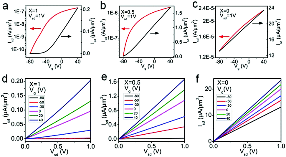 | ||
| Fig. 5 Transfer curves (Isd − Vg) and output curves (Isd − Vsd) of SnSe2(1−x)S2x FETs for (a and d) x = 1, (b and e) x = 0.5 and (c and f) x = 0. | ||
As shown in Table 2, the ‘ON/OFF’ ratio and field effect mobility of SnSe2(1−x)S2x alloys shows obviously modulation with variation of Se composition. With S atom rich phase (x = 1 and 0.75), the ‘ON/OFF’ ratio reach to 4 × 10³; while with Se rich phase (x = 0.25 and 0) the ‘ON/OFF’ ratio decrease to less than 2.86, indicating the conduction channel of the FETs gradually become heavily electron doped with the increment of Se content. The field effect mobility increase from 2.34 to 71.30 cm2 V−1 s−1 as the Se content increase from 0 to 1. With the equation of
| x value in SnSe2(1−x)S2x | μ FE (cm2 V−1 s−1) | ‘ON/OFF’ ratio |
|---|---|---|
| x = 1 | 2.34 | 4.00 × 10³ |
| x = 0.75 | 4.25 | 4.20 × 10³ |
| x = 0.5 | 10.34 | 1.00 × 10² |
| x = 0.25 | 38.24 | 2.86 |
| x = 0 | 71.30 | 1.49 |
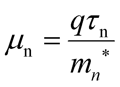
The DFT mn* at the bottom of conduction band of monolayer SnS2 and SnSe2 are calculated and list in Table 3. The value of the SnSe2mn* is smaller than SnS2mn*, which partly contribute to the higher field effect mobility for SnSe2, thus in part due to obviously bandgap modulation for SnSe2(1−x)S2x alloys with variation of Se composition. The value of the SnSe2mn* is smaller than SnS2mn*, which partly contribute to the higher field effect mobility for SnSe2, thus in part due to obviously bandgap modulation for SnSe2(1−x)S2x alloys with variation of Se composition.
| m n * [M] | m n * [K] | |
|---|---|---|
| SnS2 | 0.79m0 | 0.50m0 |
| SnSe2 | 0.64m0 | 0.45m0 |
As shown in Table 4, the modulation range of bandgap and carrier mobility of SnSe2(1−x)S2x alloys is much wider than other reported 2D alloys, which shows great potential for next-generation nanoelectronics and optoelectronics application. The SnSeS FET is also illuminated under 532 nm laser, and the transfer and output characteristics are shown in Fig. 6a and b, respectively. The transfer and output curves are obviously improved under 532 nm laser illumination, suggesting the photosensitive property of SnSeS alloy nanosheets. The light absorption causes an increment of carrier mobility (from 10.34 cm2 V−1 s−1 under dark condition to 12.16 cm2 V−1 s−1 under 532 nm laser illumination with the power of 514.6 mW cm−2) of SnSeS, showing the potential application in phototransistors. The photoconductivity spectrum of SnSeS FET is also acquired under dark and 532 nm laser illumination with Vg = 0. The photocurrent (defined as Iph = Ilight − Idark) has a strong light intensity dependence, as shown in Fig. 6c, and the experimental data is fitted by the power equation Iph ∼ Pα, where α is 0.936 here (Fig. 6d).
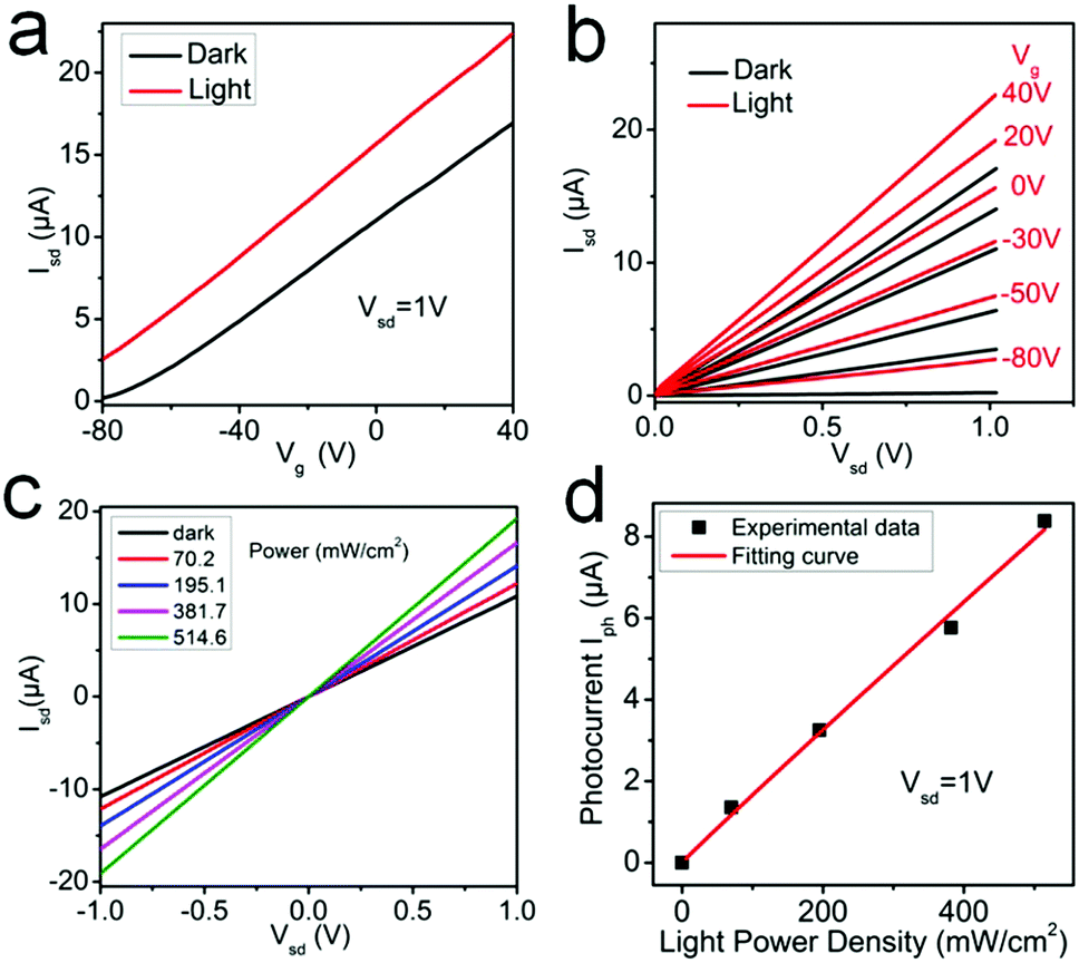 | ||
| Fig. 6 (a) Transfer (Isd − Vg) and (b) output (Isd − Vsd) characteristics of SnSeS FETs measured under dark and laser power of 514.6 mW cm−2. (c) Photoconductivity spectrum of SnSeS FET acquired at dark and various illuminated power intensities. (d) Photocurrent (defined as Iph = Ilight − Idark) as function of light power density with Vsd = 1 V. | ||
4. Conclusion
In summary, the 2D SnSe2(1−x)S2x with five different composition values (x = 0, 0.25, 0.5, 0.75 and 1, respectively) have been investigated comprehensively. The XRD and TEM results exhibit the high quality of the sample, while EDX mappings reveal a random arrangement of S and Se atoms in these 2D alloys. The UV-visible absorption spectra shows a continuously tunable bandgap of SnSe2(1−x)S2x, consistent with our DFT calculation result. Electrical transport studies further reveal that the carrier mobility of SnSe2(1−x)S2x nanosheets FETs can be obviously modulated with the changing of the alloy composition, which should partly result from the different effective mass between SnS2 and SnSe2. The carrier mobility of SnSeS FET can also be obviously increased by light illumination of 532 nm laser, indicating the potential for SnSe2(1−x)S2x nanosheets to be used as phototransistors. Our study suggests that SnSe2(1−x)S2x nanosheets is a highly qualified 2D materials for next-generation nanoelectronics and optoelectronics application.Acknowledgements
This work was financially supported by the National Natural Science Foundation of China (grant no. 61622406, 11674084, 11674310, 61571415, 51502283 and 11474273), National Key Research and Development Program of China (Grant No. 2016YFB0700700), the “Hundred Talents Program” of Chinese Academy of Sciences (CAS), and the CAS/SAFEA International Partnership Program for Creative Research Teams.Notes and references
- K. S. Novoselov, A. K. Geim, S. V. Morozov, D. Jiang, Y. Zhang, S. V. Dubonos, I. V. Grigorieva and A. A. Firsov, Science, 2004, 306, 666–669 CrossRef CAS PubMed.
- A. K. Geim, Science, 2009, 324, 1530–1534 CrossRef CAS PubMed.
- F. Wang, Z. X. Wang, Q. S. Wang, F. M. Wang, L. Yin, K. Xu, Y. Huang and J. He, Nanotechnology, 2015, 26, 26 Search PubMed.
- Q. H. Wang, K. Kalantar-Zadeh, A. Kis, J. N. Coleman and M. S. Strano, Nat. Nanotechnol., 2012, 7, 699–712 CrossRef CAS PubMed.
- M. S. Fuhrer and J. Hone, Nat. Nanotechnol., 2013, 8, 146–147 CrossRef CAS PubMed.
- B. Radisavljevic, A. Radenovic, J. Brivio, V. Giacometti and A. Kis, Nat. Nanotechnol., 2011, 6, 147–150 CrossRef CAS PubMed.
- F. Schwierz, J. Pezoldt and R. Granzner, Nanoscale, 2015, 7, 8261–8283 RSC.
- X. D. Duan, C. Wang, Z. Fan, G. L. Hao, L. Z. Kou, U. Halim, H. L. Li, X. P. Wu, Y. C. Wang, J. H. Jiang, A. L. Pan, Y. Huang, R. Q. Yu and X. F. Duan, Nano Lett., 2016, 16, 264–269 CrossRef CAS PubMed.
- Y. Chen, J. Xi, D. O. Dumcenco, Z. Liu, K. Suenaga, D. Wang, Z. Shuai, Y.-S. Huang and L. Xie, ACS Nano, 2013, 7, 4610–4616 CrossRef CAS PubMed.
- L. M. Xie, Nanoscale, 2015, 7, 18392–18401 RSC.
- Y. F. Chen, J. Y. Xi, D. O. Dumcenco, Z. Liu, K. Suenaga, D. Wang, Z. G. Shuai, Y. S. Huang and L. M. Xie, ACS Nano, 2013, 7, 4610–4616 CrossRef CAS PubMed.
- H. F. Liu, K. K. A. Antwi, S. Chua and D. Z. Chi, Nanoscale, 2014, 6, 624–629 RSC.
- Y. F. Chen, D. O. Dumcenco, Y. M. Zhu, X. Zhang, N. N. Mao, Q. L. Feng, M. Zhang, J. Zhang, P. H. Tan, Y. S. Huang and L. M. Xie, Nanoscale, 2014, 6, 2833–2839 RSC.
- Q. Fu, L. Yang, W. H. Wang, A. Han, J. Huang, P. W. Du, Z. Y. Fan, J. Y. Zhang and B. Xiang, Adv. Mater., 2015, 27, 4732–4738 CrossRef CAS PubMed.
- H. L. Li, Q. L. Zhang, X. D. Duan, X. P. Wu, X. P. Fan, X. L. Zhu, X. J. Zhuang, W. Hu, H. Zhou, A. L. Pan and X. F. Duan, J. Am. Chem. Soc., 2015, 137, 5284–5287 CrossRef CAS PubMed.
- V. Klee, E. Preciado, D. Barroso, A. E. Nguyen, C. Lee, K. J. Erickson, M. Triplett, B. Davis, I. H. Lu, S. Bobek, J. McKinley, J. P. Martinez, J. Mann, A. A. Talin, L. Bartels and F. Leonard, Nano Lett., 2015, 15, 2612–2619 CrossRef CAS PubMed.
- H. L. Li, X. D. Duan, X. P. Wu, X. J. Zhuang, H. Zhou, Q. L. Zhang, X. L. Zhu, W. Hu, P. Y. Ren, P. F. Guo, L. Ma, X. P. Fan, X. X. Wang, J. Y. Xu, A. L. Pan and X. F. Duan, J. Am. Chem. Soc., 2014, 136, 3756–3759 CrossRef CAS PubMed.
- Q. L. Feng, Y. M. Zhu, J. H. Hong, M. Zhang, W. J. Duan, N. N. Mao, J. X. Wu, H. Xu, F. L. Dong, F. Lin, C. H. Jin, C. M. Wang, J. Zhang and L. M. Xie, Adv. Mater., 2014, 26, 2648–2653 CrossRef CAS PubMed.
- Q. Gong, L. Cheng, C. Liu, M. Zhang, Q. Feng, H. Ye, M. Zeng, L. Xie, Z. Liu and Y. Li, ACS Catal., 2015, 5, 2213–2219 CrossRef CAS.
- Q. Feng, N. Mao, J. Wu, H. Xu, C. Wang, J. Zhang and L. Xie, ACS Nano, 2015, 9, 7450–7455 CrossRef CAS PubMed.
- J. Mann, Q. Ma, P. M. Odenthal, M. Isarraraz, D. Le, E. Preciado, D. Barroso, K. Yamaguchi, G. V. S. Palacio, N. Andrew, T. Tai, M. Wurch, N. Ariana, V. Klee, S. Bobek, D. Sun, T. F. Heinz, T. S. Rahman, R. Kawakami and L. Bartels, Adv. Mater., 2014, 26, 1399–1404 CrossRef CAS PubMed.
- H. Li, X. Duan, X. Wu, X. Zhuang, H. Zhou, Q. Zhang, X. Zhu, W. Hu, P. Ren, P. Guo, L. Ma, X. Fan, X. Wang, J. Xu, A. Pan and X. Duan, J. Am. Chem. Soc., 2014, 136, 3756–3759 CrossRef CAS PubMed.
- J. Jadczak, D. O. Dumcenco, Y. S. Huang, Y. C. Lin, K. Suenaga, P. H. Wu, H. P. Hsu and K. K. Tiong, J. Appl. Phys., 2014, 116, 193505 CrossRef.
- Q. Feng, Y. Zhu, J. Hong, M. Zhang, W. Duan, N. Mao, J. Wu, H. Xu, F. Dong, F. Lin, C. Jin, C. Wang, J. Zhang and L. Xie, Adv. Mater., 2014, 26, 2648–2653 CrossRef CAS PubMed.
- S. Tongay, D. S. Narang, J. Kang, W. Fan, C. Ko, A. V. Luce, K. X. Wang, J. Suh, K. D. Patel, V. M. Pathak, J. Li and J. Wu, Appl. Phys. Lett., 2014, 104, 093108 CrossRef.
- G. Su, V. G. Hadjiev, P. E. Loya, J. Zhang, S. Lei, S. Maharjan, P. Dong, P. M. Ajayan, J. Lou and H. Peng, Nano Lett., 2015, 15, 506–513 CrossRef CAS PubMed.
- G. Kiruthigaa, C. Manoharan, M. Bououdina, S. Ramalingam and C. Raju, Solid State Sci., 2015, 44, 32–38 CrossRef CAS.
- J.-H. Ahn, M.-J. Lee, H. Heo, J. H. Sung, K. Kim, H. Hwang and M.-H. Jo, Nano Lett., 2015, 15, 3703–3708 CrossRef CAS PubMed.
- D. De, J. Manongdo, S. See, V. Zhang, A. Guloy and H. B. Peng, Nanotechnology, 2013, 24, 025202 CrossRef PubMed.
- X. Zhou, L. Gan, W. M. Tian, Q. Zhang, S. Y. Jin, H. Q. Li, Y. Bando, D. Golberg and T. Y. Zhai, Adv. Mater., 2015, 27, 8035–8041 CrossRef CAS PubMed.
- Y. Huang, K. Xu, Z. X. Wang, T. A. Shifa, Q. S. Wang, F. Wang, C. Jiang and J. He, Nanoscale, 2015, 7, 17375–17380 RSC.
- Y. Su, M. A. Ebrish, E. J. Olson and S. J. Koester, Appl. Phys. Lett., 2013, 103, 263104 CrossRef.
- C. Fan, Y. Li, F. Y. Lu, H. X. Deng, Z. M. Wei and J. B. Li, RSC Adv., 2016, 6, 422–427 RSC.
- Y. C. Huang, X. Chen, D. M. Zhou, H. Liu, C. Wang, J. Y. Du, L. X. Ning and S. F. Wang, J. Phys. Chem. C, 2016, 120, 5839–5847 CAS.
- T. F. Pei, L. H. Bao, G. C. Wang, R. S. Ma, H. F. Yang, J. J. Li, C. Z. Gu, S. Pantelides, S. X. Du and H. J. Gao, Appl. Phys. Lett., 2016, 108, 053506 CrossRef.
- P. Perumal, R. K. Ulaganathan, R. Sankar, Y. M. Liao, T. M. Sun, M. W. Chu, F. C. Chou, Y. T. Chen, M. H. Shih and Y. F. Chen, Adv. Funct. Mater., 2016, 26, 3630–3638 CrossRef CAS.
- J. Yu, C. Y. Xu, Y. Li, F. Zhou, X. S. Chen, P. A. Hu and L. Zhen, Sci. Rep., 2015, 5, 17109 CrossRef CAS PubMed.
- T. S. Pan, D. De, J. Manongdo, A. M. Guloy, V. G. Hadjiev, Y. Lin and H. B. Peng, Appl. Phys. Lett., 2013, 103, 093108 CrossRef.
- F. A. S. Alalamy and A. A. Balchin, J. Cryst. Growth, 1977, 38, 221–232 CrossRef CAS.
- Y. Li, L. Huang, M. Zhong, Z. Wei and J. Li, Adv. Mater. Technol., 2016, 1, 1600001 CrossRef.
- N. Huo, J. Yang, L. Huang, Z. Wei, S.-S. Li, S.-H. Wei and J. Li, Small, 2015, 11, 5430–5438 CrossRef CAS PubMed.
- M. Zhang, J. X. Wu, Y. M. Zhu, D. O. Dumcenco, J. H. Hong, N. N. Mao, S. B. Deng, Y. F. Chen, Y. L. Yang, C. H. Jin, S. H. Chaki, Y. S. Huang, J. Zhang and L. M. Xie, ACS Nano, 2014, 8, 7130–7137 CrossRef CAS PubMed.
- C. R. Wang, K. B. Tang, Q. Yang and Y. T. Qian, Chem. Phys. Lett., 2002, 357, 371–375 CrossRef CAS.
- D. G. Mead and J. C. Irwin, Solid State Commun., 1976, 20, 885–887 CrossRef CAS.
- K. Hayashi, N. Sawaki and I. Akasaki, Jpn. J. Appl. Phys., 1991, 30, 501–505 CrossRef CAS.
- V. Y. Davydov, I. N. Goncharuk, A. N. Smirnov, A. E. Nikolaev, W. V. Lundin, A. S. Usikov, A. A. Klochikhin, J. Aderhold, J. Graul, O. Semchinova and H. Harima, Phys. Rev. B: Condens. Matter Mater. Phys., 2002, 65, 13 CrossRef.
- C. Ramkumar, K. P. Jain and S. C. Abbi, Phys. Rev. B: Condens. Matter Mater. Phys., 1996, 54, 7921–7928 CrossRef CAS.
- J. Mann, Q. Ma, P. M. Odenthal, M. Isarraraz, D. Le, E. Preciado, D. Barroso, K. Yamaguchi, G. V. Palacio, A. Nguyen, T. Tran, M. Wurch, A. Nguyen, V. Klee, S. Bobek, D. Z. Sun, T. F. Heinz, T. S. Rahman, R. Kawakami and L. Bartels, Adv. Mater., 2014, 26, 1399–1404 CrossRef CAS PubMed.
Footnote |
| † Electronic supplementary information (ESI) available. See DOI: 10.1039/c6tc03751h |
| This journal is © The Royal Society of Chemistry 2017 |