
Rewritable non-volatile stress information memory by bulk trap-induced giant piezoresistance effect in individual PbS micro/nanowires
Haiping
Shi
a,
Jianping
Zheng
a,
Baochang
Cheng
*ab,
Jie
Zhao
a,
Xiaohui
Su
b,
Yanhe
Xiao
a and
Shuijin
Lei
a
aSchool of Materials Science and Engineering, Nanchang University, 999 Xuefu Avenue, Nanchang, 330031, China. E-mail: bcheng@vip.sina.com
bNanoscale Science and Technology Laboratory/Institute for Advanced Study, Nanchang University, 999 Xuefu Avenue, Nanchang, 330031, China
First published on 1st December 2016
Abstract
Piezoresistance, induced by an applied mechanical stress, has been widely used in various sensors. Herein, individual PbS micro/nanowire-based devices were constructed on flexible insulating plastic substrates. They not only show dynamic strain-evoked giant piezoresistance (GPR) effects, but also show excellent functions for application in non-volatile piezoresistance random access memory (PRRAM). The trapped electron hopping mechanism, tuned by exerting external strain and an electric field, is proposed. Under dynamic compression/tension with a strain of ±0.26%, the gauge factor can approach four orders of magnitude, dominantly originating from the strain-induced variation of the trap barrier height within the PbS micro/nanowires. After loading both compressive and tensile strains at a low operation bias voltage, additionally, the emptying of trap states results in a down-shift of the PbS Fermi level, and correspondingly the device resistivity increases, indicating that the stress-related data can be written/set by loading different strains. Subsequently, the emptied trap states can be filled up under a relatively high external electric field so that in turn the Fermi level of PbS up-shifts, and accordingly the device resistivity restores to the initial low resistance state, that is, the stored stress-related information can be effectively erased/reset by applying a relatively high external bias voltage. The repeatable writing/erasing characteristics of nanostructure-based devices offer an avenue to develop low power and reliable non-volatile PRRAM for applications.
1. Introduction
At present, the physical critical point of the existing materials and technologies in the semiconductor field is being reached, and new technology breakthroughs in semiconductor materials are impending. Developing micro/nanoscale metal–semiconductor–metal (MSM) systems for non-volatile random access memory (RAM) is one key technological step that has attracted increasing attention in recent years.1–4 Recently, the concepts of memory have been pursued from magnetoresistive RAM (MRAM) to phase-change RAM (PCRAM).5–10 MRAM has been realized by control of the magnetic field which controls the change of the resistance in it, and PCRAM is achieved because of the thermal processes that control a phase change from the amorphous to the crystalline state in the materials.11 Yet many other types of memory devices have also been developed, such as an optoelectronic switch and memory device presented by Derycke, in which the resistance of the carbon nanotube field-effect transistors would be switched when illumination is turned on and off.12 Waser proposed electrochemical metallization memory cells, in which the memory function was achieved because of the electrode reaction and the transport kinetics.13 Cheng presented one-dimensional nanostructure-based resistive switching memories associated with interface states and bulk traps, wherein the set and reset processes can be controlled effectively by the polarity direction of the electric field.14,15 These present existing novel non-volatile resistive memories for ultrahigh density memory storage have the advantages of high density, short response time, low cost, and long endurance time.16,17Recently, a giant piezoresistance (GPR) effect, which is more than two orders of magnitude bigger than the known bulk effect, has been found in nanostructured materials under mechanical stress due to the deformation of crystal structure.18–31 Some possible GPR mechanisms have been presented to explain this behavior, such as carrier mobility variation,28 carrier effective mass variation,32 insulator-to-metal transition,33 electron concentration change,34,35 trap activation energy,36 surface Fermi level shift,37,38 and non-stress-related surface charge relaxation,39,40 however the physicochemical processes are still controversial on the nanoscale. Especially for the found PZR materials, they can immediately return to the initial resistive states once the externally applied strains are withdrawn completely. If the stress-induced piezoresistive information can be stored long term after withdrawing external strains, the materials will be promising candidates for non-volatile stress sensor and memory applications, especially for the detection of transient stress in the environment with non-real time changes, such as the potential in the micro/nanoelectromechanical system with intelligent diversified operations and in the field of seismic surveillance with the detection of strain.
Owing to a band gap of 0.41 eV and a large exciton Bohr radius of 18 nm, PbS exhibits many eminent optical and electrical properties, and hence it has been applied widely in resistive switching, non-linear optical devices, field-effect transistors, infrared detectors, and display devices.41–47 For micro/nanostructured PbS, abundant defects, which can serve as charge trap centers to produce a potential barrier, exist in the surface and interior and play a key role in conduction.48 However, their surface states can be eliminated readily via an appropriate post-annealing process, and thus their conduction is only dominated by the thermal emission rate of deep bulk traps associated with their Coulomb potential, namely Poole–Frenkel emission.41,48 Because the density-of-states (DOS) decreases with increasing energy in one-dimensional (1D) nanostructures, additionally, the same amount of charges induced by electrostatic gating can induce a greater shift in the Fermi level, resulting in greater tunability compared with the 2D, 3D, and bulk counterparts.49 Herein, two-terminal non-volatile piezoresistance RAM (PRRAM) devices, which were composed of individual PbS micro/nanowires in ohmic contact with Ag electrodes, were fabricated on flexible insulating plastic substrates. Their piezoresistance properties were investigated systematically under loading steadily static and periodically dynamic compressive and tensile strains, respectively. The results prove that the gauge factor of the devices is approached/exceeded by four orders of magnitude under exertion of both compressive and tensile strains. Of particular importance is that the devices cannot return to the initial low resistance state (LRS) after the externally applied strains are withdrawn completely, and can still remain in the high resistance state (HRS) at a low operation bias voltage. Therefore, the presence of resistance difference demonstrates that the stress-related information can be stored effectively in the system. After applying a relatively high external bias voltage without strains, more interestingly, they can return to the pristine LRS, implying that the stored stress data can be erased. Thus, the two-terminal devices based on individual PbS micro/nanowires not only can serve as highly sensitive stress sensors, but also as rewritable non-volatile stress memory.
2. Experimental
2.1 Synthesis of PbS micro/nanowires
PbS micro/nanowires were synthesized via a physical vapor deposition process based on the thermal evaporation of PbS powders which were previously prepared by a solvothermal reaction.40 Lead nitrate, sulfur powder, and ethidene diamine (solvent) were mixed in a reaction kettle, then heated up to 200 °C and maintained for 15 hours. Through the above methods, PbS powders were synthesized. Thereafter, a hollow horizontal alumina tube was installed inside a tubular furnace, the PbS powders were placed in an alumina crucible, and the catalyst was placed next to the PbS powders along to the downstream side of flowing high-purity 95% N2 + 5% H2. Before heating, the tube was maintained at a constant flow of the mixed gas of 200 sccm (standard cubic centimeters per minute) for 1 h to ensure that the O2 in the tube was eliminated. Subsequently, the furnace was heated up to 1100 °C and held for 2 h. During the growth of the PbS micro/nanowires, the gas flow was kept at a constant rate of 30 sccm. After growth, the furnace was allowed to cool to room temperature while both hydrogen and nitrogen gases continued flowing.2.2 Structure and morphology characterization of PbS micro/nanowires
The structure and morphology of the PbS micro/nanowires were investigated by means of X-ray diffraction (XRD; Phillips X'Pert PRO with Cu Kα radiation), field emission scanning electron microscopy (FESEM; FEI Quanta 200F) and high-resolution transmission electron microscopy (HRTEM; JEOL JEM-2100, operated at 200 kV).2.3 Fabrication and measurement of PRRAM device
First of all, a relatively long PbS micro/nanowire was transferred onto a flexible insulated Kapton plastic substrate and the PRRAM device was fabricated by the contact of semi-dried conducting silver paste with the two ends of the PbS wire. Then, post-annealing in a 95% N2 + 5% H2 atmosphere at 350 °C for 15 minutes was conducted to minimize the contact resistance between the Ag electrodes and PbS wire. Finally, the polydimethylsiloxane (PDMS) was coated on the device in order to increase the mechanical strength of the device. Compressive/tensile strain was attached to the devices by a linear motor, and meanwhile electrical signals were measured by a synthesized function generator (Stanford Research System Model DS345) and a low-noise current pre-amplifier (Stanford Research System Model SR570).3. Results and discussion
XRD is used to characterize the crystal structure of the as-prepared samples, as shown in Fig. 1a. It presents clear evidence that the XRD pattern corresponds to cubic PbS (JCPDS file: 65-9496). The observed peaks are induced respectively by diffraction from the (111), (200), (220), (311), (222), and (400) planes and so on, and no characteristic peaks for other impurities are observed in the XRD pattern. The morphology of the PbS samples is examined by FESEM. Fig. 1b shows a typical low-magnification FESEM image, from which a number of wire-like 1D structures can be seen apparently. These wires are randomly oriented and straight. Fig. 1c and d correspond to higher magnification FESEM images, and as shown in them, neat four-prism wires with a square cross-section are presented clearly. Fig. 1e displays a lattice-resolved TEM image of an individual nanorod, and the observed highly ordered interplanar spacings with d values of about 0.297 nm correspond to the {200} planes of PbS. The corresponding fast Fourier transform (FFT) pattern, inset in Fig. 1e, can be indexed to face-centered cubic PbS with the [100] zone axis. The compositional analysis is performed by energy dispersive X-ray spectroscopy (EDS) equipped in HRTEM, as shown in Fig. 1f, indicating that the sample is composed of Pb and S besides Cu and C from the carbon-coated TEM grid. | ||
| Fig. 1 Characterization of the as-prepared samples. (a) XRD pattern, in conformity with cubic PbS (JCPDS file: 65-9496). (b) A low-magnification FESEM image, showing the general morphology of the as-prepared samples. (c) and (d) High-magnification FESEM images, revealing the neat four-prism structure with a square cross-section. (e) HRTEM image. The inset is the corresponding FFT analysis. (f) EDS pattern. | ||
A relatively long four-prism wire was transferred on a flexible Kapton substrate and then the PRRAM device, whose schematic diagrams are inset in Fig. 2a and 3a, was fabricated by contact of semi-dried silver with the two ends of the single PbS micro/nanowire. Then PDMS was coated on the surface of the devices to increase their mechanical strength. Once the substrate was deformed, a pure strain along the horizontal axial of the PbS micro/nanowire was created because the mechanical behavior of the entire cell structure was determined by the substrate. Fig. 2a shows the I–V characteristics with an increasing steadily static compressive strain from 0 to −0.39%. The strains exerted on the PbS wires are estimated according to the following equation:50
 | (1) |
 | ||
| Fig. 2 Current response to different static compressive strains. (a) I–V characteristics with increasing static compressive strain, implying a gradual increase in conductivity. The lower right inset corresponds to the schematic representation of the device based on a single PbS wire utilized for strain response and memory measurement, and the upper left inset is the schematic illustration of the device subjected to a compressive strain. (b) Corresponding V0.5vs. ln(I/V) plots for the positive bias part in (a). (c) I–V characteristics with releasing static compressive strain, indicating a gradual decrease in conductivity. (d) Corresponding V0.5vs. ln(I/V) plots for the positive bias part in (c). | ||
 | ||
| Fig. 3 Current response to different static tensile strains. (a) I–V characteristics with increasing static tensile strain, indicating a gradual decrease in conductivity. The inset is the schematic illustration of the device subjected to a tensile strain. (b) The corresponding V0.5vs. ln(I/V) plots for the positive bias part in (a). (c) I–V characteristics with releasing static tensile strain, indicating a gradual increase in conductivity. (d) The corresponding V0.5vs. ln(I/V) plots for the positive bias part in (c). | ||
All the I–V characteristics show non-linear behavior under both loading steadily static compressive and tensile strains. To clarify the piezoresistive mechanism in the PbS micro/nanowire-based devices, the I–V curves were fitted by the Poole–Frenkel emission law.51 If this mechanism is assumed, the current through the Ag/PbS interface may be expressed as:
 | (2) |
To gain more insight into the mechanism of the piezoresistive switching under different strains, periodically dynamic compressive and tensile strains were exerted on the PbS micro/nanowire-based device under a triangle wave voltage with an amplitude of 0.5 V and a frequency of 0.005 Hz, respectively. For the concentration of trapped charges and the thermal emission rate of deep bulk traps within the PbS micro/nanowires, it is easy to reach a stable state under dynamic strains. Fig. 4a exhibits the current response to the dynamic compressive strain of about −0.26% under periodically loading for 8 s and releasing for 2 s. As seen from Fig. 4b, the conductivity of the device dramatically increases when the compressive strain is loaded, while it decreases after the strain is released. Therefore, the state under loading compressive strain can be referred to as the LRS (or ON state), and the resistance of the device is down to around 17 kΩ. In contrast, the releasing of compressive stress can be known as the HRS (or OFF state), where the resistance is up to about 18 MΩ. The OFF/ON switching ratio of resistance reaches −943, and correspondingly a gauge factor (GF) of about 3.6 × 10⁴ can be acquired by calculation with the following formula:
 | (3) |
 | ||
| Fig. 4 Plots of current response to periodically loading compressive strain of about −0.26%. (a) Under triangle wave voltage sweeping with an amplitude of 0.5 V and a frequency of 0.005 Hz, the current response to the periodic compressive strain with loading for 8 s and releasing for 2 s. (b) An enlargement of the green dotted frame in (a), showing an apparent increase of current under loading compressive strain, and the resistance is estimated to be 18 kΩ and 17 MΩ at the ON and OFF states, respectively. (c) I–V characteristics before applying a periodic dynamic compressive strain (black), and without (green curve) and with (red curve) loading static compressive strain after applying a periodic dynamic compressive strain. (d) The corresponding V0.5vs. ln(I/V) plots for the positive bias part in (c). | ||
Similarly, the I–V characteristics of the device were measured under loading a periodically dynamic tensile strain as well. Fig. 5a shows the current response to a dynamic tensile strain of about 0.26% with periodically loading for 8 s and releasing for 2 s under a triangle wave voltage. It is just opposite to the result from loading a periodically dynamic compressive strain. Fig. 5b is an enlarged view of the green dotted frame in Fig. 5a. Clearly, it can be seen that the device resistance based on a single PbS micro/nanowire increases to about 97 MΩ when a tensile strain of 0.26% is loaded, while it decreases to about 73 kΩ after the strain is completely released. Therefore, the OFF/ON switching ratio of resistance is approximately 1327, and the corresponding gauge factor is about 5.1 × 10⁴. Similarly importantly, before and after loading periodically dynamic tensile strain, the resistivity shows also a dramatic increase. In addition, the response and recovery time of the current is quite rapid when the strain is loaded and withdrawn, indicating an excellent sensitivity to external strains.
 | ||
| Fig. 5 Plots of current response to periodically loading tensile strain of about 0.26% under triangle wave voltage sweeping with an amplitude of 0.5 V and frequency of 0.005 Hz. (a) The current response to the periodic tensile strain with loading for 8 s and releasing for 2 s. (b) An enlargement of the green dotted frame in (a), showing a pronounced decrease of current upon loading tensile strain, and moreover the resistance is around 73 kΩ and 97 MΩ at the ON and OFF states, respectively. (c) I–V characteristics, without and with loading a static tensile strain after applying a periodic dynamic tensile strain. (d) The corresponding V0.5vs. ln(I/V) plots for the positive bias part in the I–V characteristics without loading any external strain after applying a periodic dynamic tensile strain. | ||
For PbS micro/nanowires, they not only show remarkable GPR behavior, but cannot return to the initial LRS after the external compressive and tensile strains are completely withdrawn. Therefore, they have incredible potential application in non-volatile PRRAM devices, in which the information can be written/set by loading external strains. The measurement results are illustrated in Fig. 6. It can be seen that the strain can induce a distinguishable and permanent resistance increase for the PbS micro/nanowires, indicating that stress information can be written/set by loading an external strain at a relatively low fixed bias voltage of 0.25 V, and read out at the similar low bias voltage of 0.25 V. It is similarly interesting that the HRS can return to the initial LRS by applying a relatively high bias voltage of 2 V without strains, demonstrating that the stored stress information can be erased effectively by applying a relatively high external bias voltage. In addition, the current can rapidly respond to the loading of external strain and high bias voltage. Fig. 6a illustrates the properties of the PRPRM cell written by a compressive strain at low operation bias voltage and erased by a relatively high bias voltage without strain. Fig. 6b corresponds to an expanded view of the dotted frame in Fig. 6a, showing a detailed current response of one read–write–read–erase–read cycle access. Before and after applying a compressive strain of about −0.52% at the low operation bias voltage of 0.25 V, the resistance difference between the HRS and LRS is around 3.5 kΩ under reading out at the same low bias voltage of 0.25 V, and the corresponding ON/OFF state resistance ratio of about 2, defined by RHRS/RLRS, can be obtained. Thereafter, the device resistance can return to its initial LRS after application of a relatively high bias voltage of 2 V without strain, and moreover the applied bias voltage is independent of polarity. In contrast, the tensile stress information can be stored into the device as well. The measurement results are illustrated in Fig. 6c and d. After the device is subjected to a tensile strain loading, its resistance increases as well. Compared with compressive strain, moreover, its resistance shows a more profound and permanent increase after completely withdrawing the external tensile strain. After applying tensile strain of about 0.26% at the bias voltage of 0.25 V, the resistance difference between the HRS and LRS is around 122 kΩ under reading out at the same bias of 0.25 V, and meanwhile a larger ON/OFF state resistance ratio of about 28 is obtained. The considerable memory window makes the device easily utilized. As compared to compressive strain, tensile strain can induce a larger memory window due to a higher OFF state resistance, and moreover the device resistances of all the steps are relatively high, indicating a low power consumption. In addition, the multiple continuous write–read–erase–read cycles in Fig. 6a and c demonstrate a high degree of reversibility and stability. Fig. 7 shows the variation of the PRRAM device resistance with time in both the HRS and LRS before and after applying compressive and tensile strains. As can be seen, the variation of their LRS and HRS resistance after 3000 seconds is found to be very little at the reading voltage of 0.25 V, respectively, confirming the non-volatile nature of the device.
 | ||
| Fig. 6 Write/read access of PRRAM cell as a stress-related memory. The blue curves correspond to the current response and the red curves represent the applied bias voltage. (a) The information is written/set by loading a compressive strain of −0.52% at a low voltage of 0.25 V, read out at the same low voltage of 0.25 V, and erased/reset by applying a relatively high voltage of 2 V. (b) The expanded view of one cycle in the green dotted frame in (a) shows a detailed write–read–erase–read cycle, revealing that the strain induces a HRS and the high bias resets a LRS. The inset, corresponding to a higher magnification, demonstrates the presence of an obvious memory window between the HRS and LRS. (c) The information is written/set by loading a tensile strain of 0.26% at a low voltage of 0.25 V, read out at the same low voltage of 0.25 V, and erased/reset by applying a relatively high voltage of 2 V. (d) The enlarged graph of the green dotted frame in (c) shows a detailed write–read–erase–read cycle. The inset associated with a higher magnification reveals the presence of a more outstanding memory window. | ||
 | ||
| Fig. 7 Stability of the PRPRM cell resistance in both the LRS and HRS, at a reading voltage of 0.25 V. (a) HRS written by compressive strain. (b) HRS written by tensile strain. | ||
To further clarify the erasing mechanism of the PRRAM cell at high bias voltage, the HRS device was consecutively swept by a triangle wave voltage with a relatively high bias magnitude of 3 V after loading strains, as shown in Fig. 8. As seen from the inset of Fig. 8, the device exhibits a non-volatile HRS at a low operation bias voltage after loading strain. With increasing external bias voltage, however, the output current of the device jumps abruptly at a voltage of about 1.5 V, switching from a HRS to LRS accompanied by a large hysteresis loop. Thus, a reset process occurs at about 1.5 V (Vreset). Afterward, when the bias voltage is swept to a positive value, the device current remains at the LRS, and moreover it is still in the LRS under the second and third cyclic sweeping, demonstrating that the device has become a LRS after it is first subjected to a voltage higher than 1.5 V. A non-volatile ON state is achieved. At low bias voltage, therefore, the stress-induced storage data can be erased effectively by applying a bias voltage higher than 1.5 V.
 | ||
| Fig. 8 After applying a strain, 3 consecutive I–V cyclic characteristics are shown with a relatively high bias voltage of 3 V, revealing the change of the device from a HRS into LRS at about −1.5 V under the first cycle. The numbered arrows (1–4) indicate the sweep direction. A current compliance of 0.64 mA is set to protect the sample from a permanent breakdown. The inset corresponds to the I–V characteristics of the HRS after applying strain. | ||
Since the work function of Ag (ΦAg = 4.26 eV) is lower than the electron affinity of PbS (χPbS = 4.6 eV),54–56 it would be expected to form ohmic contact when the n-type PbS micro/nanowire is in direct contact with the Ag electrodes. Due to the synthesis of PbS 1D structures at a high temperature of 1100 °C and the difference in the stoichiometric ratio of sulfur to lead element, the presence of interstitial lead and sulfur vacancies can serve as trap states to produce a potential barrier height (qϕ) within the PbS micro/nanowires. For the micro/nanostructures with a very large surface-to-volume ratio and typical n-type properties, additionally, quantities of dangling bonds can induce acceptor-type surface states to exist due to the breaking of lattice periodicity on their surfaces. Nevertheless, the surface states between the PbS wire and Ag electrode can be eliminated effectively by a proper post-annealing process.41 Thus, only deep bulk-related trap states are dominant for the PbS-based devices. Inside the PbS micro/nanowires, quantities of singly charged VS+ and doubly charged VS++ deep level defects, serving as positively charged trap states, can capture electrons and then change into neutral VS [VS++ + 2e− → VS and VS+ + e− → VS]. Conversely, the captured electrons can also escape from the trap states with the variation of the external environment, resulting in a reformation of VS+ and VS++. For the nanostructure lattice with a small size, it is easier to deform under loading an external stress. For the internal bulk trap states of the nanostructure, therefore, the ability of capture charges will be subjected to a strong influence on external stress. It is expected that the trap barrier height (qϕ) and captured electron population could be modulated effectively by the strain-induced injection of electrons from/into bulk trap states.
At zero bias voltage or a low bias voltage (V < ϕ), the height (qV) of the energy band or Fermi level (Ef) tilt induced by the externally applied bias voltage is lower than that of the trap barrier (qϕ). The influence of the external electric field on the trapped electrons can be ignored. When a compressive strain is exerted on the PRRAM cell, illustrated schematically in Fig. 9b, a pure compressive strain along the horizontal axial of the PbS wire will be created and the lattice will be compressed. The trap barrier height (qϕC) will decrease compared to that without strain (qϕ). It will be easier for electrons to hop from one trap to another or the CB at a given low bias voltage, resulting in an increase of the free electron density. For a specific semiconductor such as PbS, its Ef is mainly dependent on the free electron density.57 Correspondingly, the Fermi level (Ef,compressive strain) of PbS up-shifts compared to that without strain (Ef,without strain) and the conductivity of the devices increases. When a tensile strain is exerted on the PRRAM cell at the same low bias voltage (V < ϕ), in contrast, the lattice will be stretched and the trap barrier height (qϕT) will increase compared to that without strain (qϕ), and hence it will be more difficult for electrons to hop from trap states. It needs higher energy to extract electrons from trap states. Compared to that without strain (Ef,without strain), the Fermi level (Ef,compressive strain) of PbS down-shifts, and therefore the conductivity of the devices reduces due to the decrease of the free electron concentration.
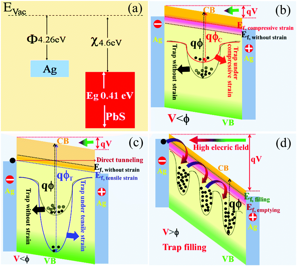 | ||
| Fig. 9 Schematic diagram of strain-induced variation of the trap barrier height and captured electron population for illustrating the giant piezoresistance-related memory effect. qϕ, qϕC, and qϕT represent the trap barrier height without strain, under compressive strain, and under tensile strain, respectively. V corresponds to the externally applied bias voltage. Ef,without strain, Ef,compressive strain, Ef,tensile strain, Ef,filling, and Ef,emptying represent respectively the relative position of the n-type non-degenerate PbS Fermi level under the states of no strain, compressive strain, tensile strain, filling, and emptying. CB and VB correspond to the conduction band and valence band of PbS, respectively. (a) Energy band diagram before contact of Ag and PbS, showing that the work function of Ag is less than the electron affinity of PbS. (b) Under low operation bias voltage (V < ϕ) and compressive strain, the trap barrier height (qϕC) decreases compared to that without strain (qϕ). It is easier for the trapped electrons to hop from traps. Therefore, the Fermi level up-shifts and the device conductivity increases. Additionally, the total number of trapped electrons decreases under the mechanical stimuli of compression, namely the detrapping effect, resulting in a HRS after loading a compressive strain. (c) Under low operation bias voltage (V < ϕ) and tensile strain, the trap barrier height (qϕT) increases compared to that without strain (qϕ). It is more difficult for the trapped electrons to hop from traps. Therefore, the Fermi level down-shifts and the device conductivity decreases. Additionally, the population of trapped electrons decreases similarly under the mechanical stimuli of tension, resulting in a HRS after loading tensile strain. (d) At a relatively high bias voltage (V > ϕ), the height of the energy band or Fermi level tilt (qV) is larger than that of the trap barrier (qϕ), and the emptied trap states are filled up, resulting in an up-shift of the Fermi level compared to that with an emptied HRS. Therefore, the device transforms from a HRS into a LRS and the stored stress information is erased. | ||
Although the device conductivity increases upon exerting compressive strain, it both decreases after completely removing tensile or compressive strains. This indicates that the captured electrons can escape from traps by the mechanical stimuli of tension and compression, namely deformation-induced detrapping.58–61 When the compressive or tensile stress load is applied, the crystal lattice of PbS deforms. The trapped electrons can obtain mechanical energy and then escape from the traps under the action of mechanical stimuli. The total number of trapped charges decreases and the trap states are emptied after the loaded strains are withdrawn completely, resulting in a decrease of trapped electron hopping probability. Consequently, the Fermi level (Ef,emptying) of the PbS micro/nanowires down-shifts, and the conductivity of the device decreases due to the reduction of the free electron concentration, resulting in a HRS. For tensile strains, they can induce the device resistance to increase more remarkably than compressive strains, indicating that the detrapping effect is more pronounced which in turn decreases largely the population of trapped charges. After completely withdrawing strains, the population of trapped charges cannot return to the high density of the initial states at a given low bias voltage, and therefore the device shows a HRS. With increasing external bias voltage, subsequently, the energy band tilts gradually and then becomes triangular, and meanwhile the trap barrier height decreases.62 When the height of the energy band or Fermi level tilt is larger than that of the trap barrier (qV > qϕ) without external strains, illustrated schematically in Fig. 9d, electrons can be injected into the emptied traps from the negative electrode, resulting in a filling of trap states. At an external bias voltage higher than a certain value (>1.5 V), the current of the HRS device jumps abruptly and increases rapidly, and then the device changes into a LRS, as illustrated in Fig. 8. This result provides a substantial support for this view of trap emptying and filling. Due to the increase of the relative population of trapped electrons, it is easier for the trapped electrons to hop from one trap center to another or the CB. Especially when the trap states are completely filled up, the free electron density significantly increases and in turn the Fermi level (Ef,filling) of the PbS micro/nanowires up-shifts compared with the emptied states (Ef,emptying), and the devices can return to the pristine LRS. Correspondingly, the conduction mechanism changes from typical PF emission to quasi-ohmic. It is due to the emptying/filling or discharging/charging of trapped states that the stress-related information can repeatedly be written by exerting an appropriate strain at a low bias voltage (V < ϕ) and then erased by applying a relatively high bias voltage (V > ϕ) without strains. Based on the analysis above, the PRRAM mechanism in the two-terminal Ag–PbS–Ag devices could be illustrated schematically in Fig. 9.
4. Conclusions
In summary, individual PbS micro/nanowire-based two-terminal devices not only show remarkable GPR behavior but show rewritable non-volatile PRRAM effect. Upon loading compressive strain, the conductivity of the devices increases significantly. Conversely, their conductivity decreases dramatically upon loading tensile strain. Especially under a dynamic tensile or compressive strain of about ±0.26%, the gauge factor approaches four orders of magnitude. It dominantly originates from the tensile strains inducing the trap barrier height to increase whereas compressive strains induce it to decrease, giving rise to a variation in the probability of electron hopping from one trap to another or the CB, which in turn tunes the electrical conductivity. More importantly, when the tensile and compressive stress load is applied to the PbS micro/nanowires, a detrapping effect can occur due to mechanical stimuli at a low operation bias voltage (V < ϕ), resulting in the emptying of the trap states after loading strains. Especially for tensile strain, it can induce the total number of trapped charges to decrease more strikingly. Accordingly, the Fermi level of PbS down-shifts and the device transforms into a HRS due to the decrease of free electron concentration. Thus, the stress-related information can be written/set effectively by loading an appropriate strain at zero or relatively low bias voltage. However, the emptied trap states can be filled up by applying a relatively high bias voltage (V > ϕ) without strains, and therefore the devices can return to the initial LRS states resulting from the up-shift of the PbS Fermi level induced by the increase of the free electron concentration. The stored stress information can be effectively erased/reset by a relatively high external bias voltage. The PbS micro/nanowires with highly repeatable and stable writing/erasing properties show great potential for versatility in non-volatile stress sensors and memory applications, especially for the detection of transient stress in the environment with non-real time changes.Acknowledgements
This work was financially supported by the National Natural Science Foundation of China (51462023, 51571107, 51162023), the Project for Young Scientist Training of Jiangxi Province (20133BCB23002), and the Major Program of Natural Science Foundation of Jiangxi Province (20152ACB20010).Notes and references
- B. K. You, W. I. Park, J. M. Kim, K. I. Park, H. K. Seo, J. Y. Lee, Y. S. Jung and K. J. Lee, ACS Nano, 2014, 8, 9492 CrossRef CAS PubMed.
- L. Liang, K. Li, C. Xiao, S. J. Fan, W. S. Zhang, W. H. Xu, W. Tong, J. Y. Liao and Y. Y. Zhou, J. Am. Chem. Soc., 2015, 137, 3102 CrossRef CAS PubMed.
- G. Wang, Y. Yang, J. H. Lee, V. Abramova, H. L. Fei, G. D. Ruan, E. L. Thomas and J. M. Tour, Nano Lett., 2014, 14, 4694 CrossRef CAS PubMed.
- Y. C. Huang, P. Y. Chen, K. F. Huang, T. C. Chuang, H. H. Lin, T. S. Chin, R. S. Liu, Y. W. Lan, C. D. Chen and C. H. Lai, NPG Asia Mater., 2014, 6, e85 CrossRef CAS.
- Z. G. Wang, Y. Zhang, Y. J. Wang, Y. X. Li, H. S. Luo, J. F. Li and D. Viehland, ACS Nano, 2014, 8, 7793 CrossRef CAS PubMed.
- J. M. Hu, Z. Li, L. Q. Chen and C. W. Nan, Nat. Commun., 2011, 2, 553 CrossRef PubMed.
- B. H. Mun, B. K. You, S. R. Yang, H. G. Yoo, J. M. Kim, W. I. Park, Y. Yin, M. Byun, Y. S. Jung and K. J. Lee, ACS Nano, 2015, 9, 4120 CrossRef CAS PubMed.
- W. I. Park, J. M. Kim, J. W. Jeong, Y. H. Hur, Y. J. Choi, S. H. Kwon, S. Hong, Y. Yin, Y. S. Jung and K. H. Kim, Chem. Mater., 2015, 27, 2673 CrossRef CAS.
- T. H. Lee, D. Loke, K. J. Huang, W. J. Wang and S. R. Elliott, Adv. Mater., 2014, 26, 7493 CrossRef CAS PubMed.
- C. Rios, P. Hosseini, C. D. Wright, H. Bhaskaran and W. H. P. Pernice, Adv. Mater., 2014, 26, 1372 CrossRef CAS PubMed.
- R. Waser and A. Masakazu, Nat. Mater., 2007, 6, 833 CrossRef CAS PubMed.
- J. Borghetti, V. Derycke, S. Lenfant, P. Chenevier, A. Filoramo, M. Goffman, D. Vuillaume and J. Bourgoin, Adv. Mater., 2006, 18, 2535 CrossRef CAS.
- I. Valov, R. Waser, J. R. Jameson and M. N. Kozicki, Nanotechnology, 2011, 22, 254003 CrossRef PubMed.
- B. C. Cheng, Z. Y. Ouyang, C. Chen, Y. H. Xiao and S. J. Lei, Sci. Rep., 2013, 3, 3249 Search PubMed.
- M. H. Cao, B. C. Cheng, L. Xiao, J. Zhao, X. H. Su, Y. H. Xiao and S. J. Lei, J. Mater. Chem. C, 2015, 3, 5207 RSC.
- R. Waser, R. Dittmann, G. Staikov and K. Szot, Adv. Mater., 2009, 21, 2632 CrossRef CAS.
- S. H. Jo, K. H. Kim and L. Wei, Nano Lett., 2009, 9, 870 CrossRef CAS PubMed.
- R. R. He and P. D. Yang, Nat. Nanotechnol., 2006, 1, 42 CrossRef CAS PubMed.
- J. S. Milne, A. C. H. Rowe, S. Arscott, C. Renner and J. S. Milne, Phys. Rev. Lett., 2010, 105, 226802 CrossRef CAS PubMed.
- T. K. Kang, Nanotechnology, 2012, 23, 475203 CrossRef PubMed.
- T. W. Tombler, C. W. Zhou, L. Alexseyev, J. Kong, H. J. Dai, L. Lei, C. S. Jayanthi, M. J. Tang and S. Y. Wu, Nature, 2000, 405, 769 CrossRef CAS PubMed.
- E. D. Minot, Y. Yaish, V. Sazonova, J. Y. Park, M. Brink and P. L. McEuen, Phys. Rev. Lett., 2003, 90, 156401 CrossRef CAS PubMed.
- X. Chen, X. H. Zheng, J. K. Kim, X. X. Li and D. W. Lee, J. Vac. Sci. Technol., B, 2011, 29, 06FE01 Search PubMed.
- J. Cao, Q. Wang and H. Dai, Phys. Rev. Lett., 2003, 90, 157601 CrossRef PubMed.
- J. M. Gray, K. A. Bertness, N. A. Sanford and C. T. Rogers, Appl. Phys. Lett., 2012, 101, 233115 CrossRef.
- J. Greil, A. Lugstein, C. Zeiner, G. Strasser and E. Bertagnolli, Nano Lett., 2012, 12, 6230 CrossRef CAS PubMed.
- G. Hwang, H. Hashimoto, D. J. Bell, L. Dong, B. J. Nelson and S. Schon, Nano Lett., 2009, 9, 554 CrossRef CAS PubMed.
- F. M. Gao, J. Y. Zheng, M. F. Wang, G. D. Wei and W. Y. Yang, Chem. Commun., 2011, 47, 11993 RSC.
- X. Li, X. L. Wei, T. T. Xu, D. Pan, J. H. Zhao and Q. Chen, Adv. Mater., 2015, 27, 2852 CrossRef CAS PubMed.
- T. D. Gupta, T. Gacoin and A. C. H. Rowe, Adv. Funct. Mater., 2014, 24, 4522 CrossRef.
- J. Park, Y. Lee, J. Hong, M. Ha, Y. Jung, H. Lim, S. Y. Kim and H. Ko, ACS Nano, 2014, 8, 4689 CrossRef CAS PubMed.
- J. X. Cao, X. G. Gong and R. Q. Wu, Phys. Rev. B: Condens. Matter Mater. Phys., 2007, 75, 233302 CrossRef.
- M. Copel, M. A. Kuroda, M. S. Gordon, X. H. Liu, S. S. Mahajan, G. J. Martyna, N. Moumen, C. Armstrong, S. M. Rossnagel, T. M. Shaw, P. M. Solomon, T. N. Theis, J. J. Yurkas, Y. Zhu and D. M. Newns, Nano Lett., 2013, 13, 4650 CrossRef CAS PubMed.
- Y. L. Yang and X. X. Li, IEEE Electron Device Lett., 2011, 32, 411 CrossRef CAS.
- Y. L. Yang and X. X. Li, Nanotechnology, 2011, 22, 015501 CrossRef PubMed.
- Y. S. Choi, T. Nishida and S. E. Thompson, Appl. Phys. Lett., 2008, 92, 173507 CrossRef.
- A. C. H. Rowe, Nat. Nanotechnol., 2008, 3, 311 CrossRef CAS PubMed.
- T. T. Nghiem, V. Aubry-Fortuna, C. Chassat, A. Bosseboeuf and P. Dollfus, Mod. Phys. Lett. B, 2011, 25, 995 CrossRef CAS.
- J. S. Milne, A. C. H. Rowe, S. Arscott and C. Renner, Phys. Rev. Lett., 2010, 105, 226802 CrossRef CAS PubMed.
- E. Anderas, L. Vestling, J. Olsson and I. Katardjiev, Procedia Chem., 2009, 1, 80 CrossRef.
- J. P. Zheng, B. C. Cheng, F. Z. Wu, X. H. Su, Y. H. Xiao, R. Guo and S. J. Lei, ACS Appl. Mater. Interfaces, 2014, 6, 20812 CAS.
- T. Kawawaki, H. B. Wang, T. Kubo, K. Saito, J. Nakazaki, H. Segawa and T. Tatsuma, ACS Nano, 2015, 9, 4165 CrossRef CAS PubMed.
- S. Yakunin, D. N. Dirin, L. Protesescu, M. Sytnyk, S. Tollabimazraehno, M. Humer, F. Hackl, T. Fromherz, M. I. Bodnarchuk and M. V. Kovalenko, ACS Nano, 2014, 8, 12883 CrossRef CAS PubMed.
- N. Kholmicheva, P. Moroz, U. Rijal, E. Bastola, P. Uprety, G. Liyanage, A. Razgoniaev, A. D. Ostrowski and M. Zamkov, ACS Nano, 2014, 8, 12549 CrossRef CAS PubMed.
- J. Schornbaum, Y. Zakharko, M. Held, S. Thiemann, F. Gannott and J. Zaumseil, Nano Lett., 2015, 15, 1822 CrossRef CAS PubMed.
- G. J. Supran, K. W. Song, G. W. Hwang, R. E. Correa, J. Scherer, E. A. Dauler, Y. Shirasaki, M. G. Bawendi and V. Bulovic, Adv. Mater., 2015, 27, 1437 CrossRef CAS PubMed.
- N. J. Thompson, M. W. B. Wilson, D. N. Congreve, P. R. Brown, J. M. Scherer, T. S. Bischof, M. F. Wu, N. Geva, M. Welborn and T. Van Voorhis, Nat. Mater., 2014, 13, 1039 CrossRef CAS PubMed.
- J. Frenkel, Phys. Rev., 1938, 54, 647 CrossRef.
- C. H. Liu, C. C. Wu and Z. H. Zhong, Nano Lett., 2011, 11, 1782 CrossRef CAS PubMed.
- J. Choi, K. Cho and S. Kim, Jpn. J. Appl. Phys., 2011, 50, 22 Search PubMed.
- J. G. Simmons, J. Phys. D: Appl. Phys., 1971, 4, 613 CAS.
- J. R. Yeargan and H. L. Taylor, J. Appl. Phys., 1968, 39, 5600 CrossRef CAS.
- H. E. Zhang, J. Miller and E. T. Yu, J. Appl. Phys., 2006, 99, 023703 CrossRef.
- G. Guizzett, F. Filippin, E. Reguzzon and G. Samoggia, Phys. Status Solidi A, 1971, 6, 605 CrossRef.
- R. A. Knapp, Phys. Rev., 1963, 132, 1891 CrossRef CAS.
- B. R. Hyun, Y. W. Zhong, A. C. Bartnik, L. Sun, H. D. Abrun, F. W. Wise, J. D. Goodreau, J. R. Matthews, T. M. Leslie and N. F. Borrell, ACS Nano, 2008, 2, 2206 CrossRef CAS PubMed.
- S. M. Sze and K. K. Ng, Physics of Semiconductor Devices, John Wiley & Sons Press, 2007 Search PubMed.
- S. Timilsina, J. S. Kim, J. Kim and G. Kim, Int. J. Precis. Eng. Manuf., 2016, 17, 1237 CrossRef.
- D. Tu, C. N. Xu, Y. Fujio and A. Yoshida, Light: Sci. Appl., 2015, 4, e356 CrossRef CAS.
- B. P. Chandra, V. K. Chandra and P. Jha, Phys. B, 2015, 461, 38 CrossRef CAS.
- B. P. Chandra, C. N. Xu, H. Yamada and X. G. Zheng, J. Lumin., 2010, 130, 442 CrossRef CAS.
- F. Vietmeyer, T. Tchelidze, V. Tsou, B. Janko and M. Kuno, ACS Nano, 2012, 6, 9133 CrossRef CAS PubMed.
| This journal is © The Royal Society of Chemistry 2017 |