
 Open Access Article
 This Open Access Article is licensed under a Creative Commons Attribution-Non Commercial 3.0 Unported Licence
Tetrabutylammonium cations for moisture-resistant and semitransparent perovskite solar cells†
Isabella
Poli
 *ac,
Salvador
Eslava
bc and
Petra
Cameron
*ac
*ac,
Salvador
Eslava
bc and
Petra
Cameron
*ac
aDepartment of Chemistry, University of Bath, Bath BA2 7AY, UK. E-mail: i.poli@bath.ac.uk; p.j.cameron@bath.ac.uk
bDepartment of Chemical Engineering, University of Bath, Bath BA2 7AY, UK
cCentre for Sustainable Chemical Technologies, University of Bath, Bath BA2 7AY, UK
First published on 17th October 2017
Abstract
Perovskite solar cells have gained increasing interest, especially after reaching performances which are comparable with mature silicon PV technologies. However, the perovskite crystalline structure CH3NH3PbI3 is unstable in the presence of moisture, which leads to fast degradation under ambient conditions. The commercialisation of perovskite solar cells will only be achieved with the engineering of long term stable materials. We report a modified perovskite absorber layer obtained by adding methylammonium iodide (MAI) and tetrabutylammonium (TBA) iodide. The incorporation of TBA improves the film coverage, reducing the number of pinholes. X-ray diffraction analysis suggests that, in common with other mixed larger cation perovskites, two distinct phases coexist: a 3D perovskite material and a 2D layered material. The TBA containing perovskite films showed improved hydrophobicity, which contributed to significantly higher moisture stability. The cells maintained their original PCE after 45 days under ambient conditions without encapsulation. In comparison, the CH3NH3PbX3 3D perovskite device lost more than 60% of its original efficiency over the same time.
Introduction
Methylammonium lead halide perovskite is a promising material for the development of cheap, solution processed solar cells. Since the emergence of perovskite solar cells in 2012,1,2 improvements in film morphology and fabrication techniques have lead to a power conversion efficiency (PCE) of 22.1%.3 Some of the properties that allow halide perovskites to be so efficient in photovoltaic applications are their good absorption of light in the visible range, long electron and hole lifetimes and optoelectronic tunability.4 A lot of research has focused on thin film fabrication to improve morphology and device reproducibility. Different lead sources have been investigated5–8 and solvent engineering strategies developed to improve perovskite crystallinity.9 These approaches have helped to increase the PCE of halide perovskite solar cells rapidly.A big challenge that remains is to ensure the long term stability of perovskite solar cells under ambient conditions. Perovskite materials suffer from very fast degradation when exposed to water or even moisture in the air.10 Leguy et al. showed that moisture in air induces a hydration process in CH3NH3PbI3, which causes strong current drops and voltage losses.11 These losses can be reversed according to eqn (1).
| 4(CH3NH3)PbI3 + 4H2O ⇌ 4[CH3NH3PbI3·H2O] ⇌ (CH3NH3)4PbI6·2H2O + 3PbI2 + 2H2O | (1) |
However, high excess of water results in a permanent dissolution of the methylammonium cation and irreversible degradation of the perovskite structure (eqn (2)).11
 | (2) |
Over the last few years a number of strategies, summarised in Fig. 1, have been developed to improve the moisture stability of perovskite solar cells (PSCs). The first strategy is encapsulation: a selection of sealing materials with good high temperature performance19 can protect the PSC and allow it to remain chemically stable20 under normal working conditions. However, encapsulation leads to considerably higher fabrication costs.
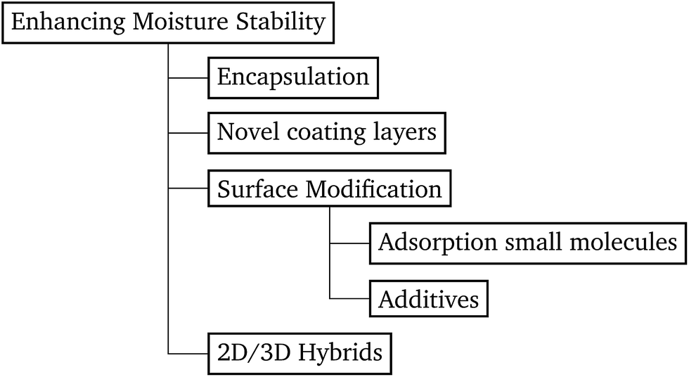 | ||
| Fig. 1 Diagram which summarizes the approaches found in the literature to limit the moisture instability of perovskite solar cells. | ||
A second strategy to improve stability is by introducing new coating layers in the structure. In 2014 the organic HTM spiro-OMeTAD was replaced with a conducting carbon nanotube–polymethylmethacrylate (PMMA) composite for the first time.21 This novel layer was mainly introduced to mitigate thermal degradation. The adopted PMMA–nanotube composite HTM was found to protect the perovskite structure and seal in volatile components more efficiently than the commonly employed HTM spiro-OMeTAD, due to its nonhygroscopic nature.21 More recently, fluorinated photo-polymer coatings22 and hydrophobic polymers, such as poly(4-vinylpyridine),23 which form strong hydrophobic barriers, have been reported. The coating was deposited on top of the perovskite film once it was dried.
A third way of enhancing moisture stability is through the use of small molecules adsorbed to the surface of the perovskite crystallites in the film. Young et al. showed how alkyl ammonium cations can be used to functionalise the perovskite surface. Perovskite films were dipped into alkyl ammonium iodide solution, improving the humidity tolerance and passivating surface defects.24 Li et al. used 2-aminoethanethiol (2-AET) as a ligand for MAI and PbI2, adding it into the perovskite precursor solution. The strong coordination interaction of PbI2–2-AET–(MAI) generated a very efficient barrier layer, which protected the perovskite crystal structure for over 10 minutes after immersion in water.25 A similar approach was reported by Sun et al., who added 2-pyridylthiourea in the perovskite precursor solution, achieving high conversion efficiencies and relatively better stability.26 The implementation of these interlayers delayed perovskite degradation.
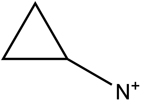
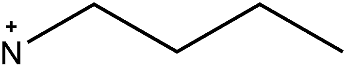
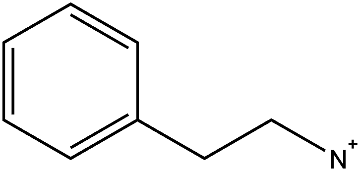
The fourth and final approach is very promising as it has been shown to create perovskite solar cells that are stable for up to one year17 and importantly achieves comparable performances to the standard 3D perovskite device. In this approach 2D/3D perovskite hybrids are prepared. Several cations have been investigated to make these 2D/3D hybrid structures, which are listed in Table 1. The first layered 2D/3D perovskite used as an absorber layer was reported in 2014 by Smith et al., using phenylethylammonium (PEA).16 Devices containing (PEA)2(MA)2Pb3I10 showed enhanced moisture stability, but poor power conversion efficiency (the best performing cell had a PCE of 4.73%). Later on, Tsai et al. overcame the issue of poor efficiency, reporting a 12.52% efficient device using n-butylammonium (BA) spacer cations in a mixed 2D/3D hybrid structure.15 Very recently, a protonated salt of aminovaleric acid iodide (AVAI) was added to the precursor solution, showing much higher moisture resistivity in standard devices and one-year stability in carbon-based solar cells.17 Grancini et al. suggested that a 2D/3D junction is generated at the TiO2/perovskite interface when AVAI is added,17 allowing the creation of carbon-based PSCs with impressive stability. It is worth noting that the XRD patterns of the AVAI/MAI mixed perovskites used to fabricate the solar cells do not show evidence of low dimensional perovskite being formed as is seen by others.12,13 The authors claimed that the 2D layer was too thin to be observed; however, it could also suggest that AVAI is concentrated in the grain boundaries, modifying the crystal structure, instead of generating a 2D/3D junction at the interface. Ma et al. reported a 2D perovskite capping layer, which allowed an increase in moisture tolerance while still keeping high conversion efficiency of a 3D absorber layer.12 A solution of cyclopropylammonium iodide (CAI) was spin coated on top of the formed 3D perovskite layer, generating a 2D/3D CA2PbI4/CH3NH3PbIxCl3−x perovskite interface at the perovskite/spiro-OMeTAD junction.
| Additive | Name | Enhancement | Ref. |
|---|---|---|---|
|
Cyclopropylammonium | • 2D/3D interface | 12 |
| • Higher efficiency and improved moisture resistance | |||
|
n-Butylamine | • 2D/3D layered perovskite absorber layer | 13–15 |
| • 12.52% efficiency and greater tolerance to high RH | |||
|
Phenylethylammonium | • First 2D/3D layered perovskite absorber layer | 16 |
|
5-Ammonium valeric acid | • 2D/3D perovskite junction | 17 |
| • 1 year stability | |||
|
Polyethyleneimine | • 2D materials in the final structure | 18 |
| • Higher absorption and slower degradation in air |
Tetrabutylammonium (TBA) and other tetraalkylammonium cations have been extensively exploited for their amphiphilic properties in the crystallisation and templating of zeolites and other porous materials.27 In perovskite solar cells, TBA is one of the alkyl ammonium cations that have been recently used as a moisture tolerant small molecule to functionalise the perovskite surface. Pre-formed perovskite films were dipped in a solvent containing TBA and the alkyl ammonium cations assembled on top of the perovskite films. The humidity tolerance of the film was improved, although solar cells based on these films were not fabricated.24 Until now, TBA has been used as a processing additive to prepare perovskites only once. It was found that introducing the tetrabutylammonium iodide salt into the perovskite precursor solution increased the coverage and reduced the pinhole size.28 It was speculated that TBA formed a layered organic–inorganic structure but no evidence was shown in the XRD pattern. Furthermore, solar cells prepared by adding only 1 wt% of TBA into the precursor solution showed very poor PCE of 1.4%.28
In this work, MAI is partly substituted with TBA using different molar percentage concentrations. We show that TBA can be used as an ionic additive in the precursor solution to enhance the stability of the final device. X-ray diffraction (XRD) analysis suggests the coexistence of two distinct phases: a 3D perovskite layer and a 2D layered perovskite. TBA might be pushed towards the surface of perovskite grains, generating 2D sheets and intra-layers at the perovskite/spiro interface. Mixed 2D/3D structures show comparable photovoltaic performance to standard 3D MAPbX3, with PCEs over 10%. Above all, they show better stability compared to the reference device. Higher water contact angles were measured for mixed cation films, which might contribute to the greater moisture stability. When aged in the dark, under ambient conditions (40 ± 20% relative humidity), the PCE for the TBA containing devices was found to be unchanged after over 40 days.
Experimental
Materials
CH3NH3I (MAI) was bought from Dyesol Australia. PbI2, PbCl2 and tetrabutylammonium (TBA) iodide were all bought from Sigma-Aldrich. The standard perovskite precursor solutions were prepared by dissolving MAI, PbI2 and PbCl2 in N,N-dimethylformamide (DMF, anhydrous, Sigma-Aldrich) to get 40 wt% solution (MAI![[thin space (1/6-em)]](https://www.rsc.org/images/entities/char_2009.gif) :PbI2:PbCl2 – 4:1:1). TBA iodide was added into the perovskite precursor solutions. Cation A was partly substituted with TBA instead of MAI with different molar percentage concentrations TBA%:MAI% (1:99, 3:97, 5:95, 10:90, 30:70, 100:0). As the concentration of I and Cl in the perovskite film is uncertain, the representations MAPbX3, (TBA)n(MA)1−nPbX3 and (TBA)PbX3 are used in the text.
:PbI2:PbCl2 – 4:1:1). TBA iodide was added into the perovskite precursor solutions. Cation A was partly substituted with TBA instead of MAI with different molar percentage concentrations TBA%:MAI% (1:99, 3:97, 5:95, 10:90, 30:70, 100:0). As the concentration of I and Cl in the perovskite film is uncertain, the representations MAPbX3, (TBA)n(MA)1−nPbX3 and (TBA)PbX3 are used in the text.
The electron transport material solution consisted of 200 mM titanium diisopropoxide bis(acetylacetonate) in ethanol. The hole transport material solution consisted of 85 mg ml−1 spiro-OMeTAD (Sigma-Aldrich) in chlorobenzene, with additives of 30 μL mL−1 of t-butyl pyridine (Sigma Aldrich) and Li-TFSI.
Solar cell fabrication
FTO glass (Sigma-Aldrich) was etched with zinc powder and HCl. It was then cleaned in 2 vol% Hellmanex solution in water, followed by deionised water, acetone, propan-2-ol and ethanol.A compact TiO2 layer was deposited by spray pyrolysis, using a hand-held atomiser to spray the solution onto the substrates held at 500 °C. Substrates were then sintered at this temperature for 10 minutes. A mesoporous TiO2 layer (2:7 weight mixture of Dyesol's 30NRD TiO2 paste in ethanol) was spun onto the TiO2 compact layer and annealed for 15 minutes at 150 °C and then a further 30 minutes at 500 °C. After cooling, substrates were subjected to UV ozone treatment for 30 minutes. Perovskite deposition was performed in a nitrogen filled glove box, following a one-step method. 100 μL of precursor solution was spun onto the substrate at 4000 rpm for 30 seconds, and then dried at 100 °C for 90 minutes. Spiro solution was spun onto the perovskite film at 3000 rpm for 30 seconds. To establish the contacts, a 2 mm wide channel of perovskite was removed from the centre of the substrate. Finally, a 100 nm thin layer of gold was thermally evaporated using evaporation masks to have 6 pixels of 0.0625 cm−2.
Characterisation
 .
.
Results and discussion
Perovskite solutions of (TBA)n(MA)1−nPbX3 with n = 0, 0.01, 0.03, 0.05, 0.1, 0.3 and 1 were used to fabricate thin films, in such a way that some of the MA cations are partially or entirely substituted with TBA cations. The growth characteristics, optical properties and film morphology were investigated. Fig. 2 shows the chemical structure of the TBA ion. In Table 2, the ionic radii of cations commonly used in organic–inorganic perovskite materials are listed. Formamidinium (FA) and methylammonium (MA) have similar size and they are considerably bigger than caesium. When one of these cations or mixtures of them are used to generate perovskite materials, a tetragonal 3D structure is created. The ionic radius of (C4H9)4N+ (TBA) is considerably larger. Being such a big cation, it is more likely to form a 2D perovskite structure, like the one created by using n-butylammonium cations.15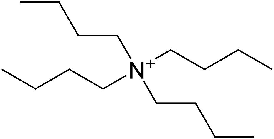 | ||
| Fig. 2 Chemical structure of the tetrabutylammonium (TBA) cation. | ||
Structural properties
X-ray diffraction (XRD) measurements of 2D/3D hybrid perovskite films found in the literature showed consistent peaks at low angles (2θ < 10 °C).12,13,17,18Fig. 3 shows XRD patterns of thin films made with (TBA)n(MA)1−nPbX3 solutions, with n = 0, 0.01, 0.03, 0.05, 0.1, 0.3 and 1 (from the bottom to the top).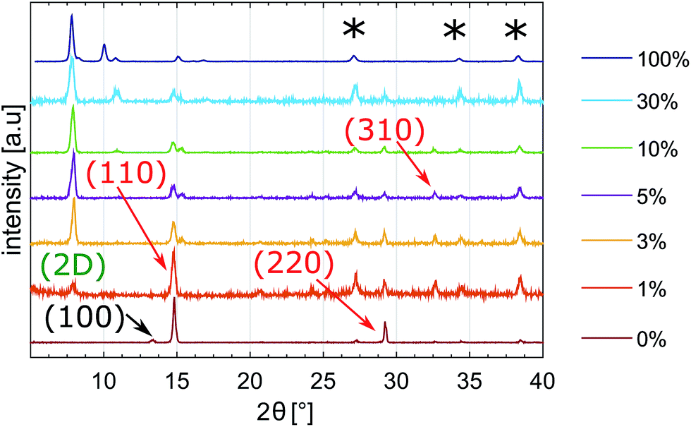 | ||
| Fig. 3 XRD patterns of (TBA)n(MA)1−nPbX3, from perovskite precursor solutions with n = 0 (0%), 0.01 (1%), 0.03 (3%), 0.5 (5%), 0.1 (10%), 0.3 (30%) and 1 (100%) respectively. Films have spun onto FTO c-glass substrates. Peaks that originated from the SnO2 underlayer are marked by asterisks. | ||
XRD patterns reveal that the perovskite structure changes considerably when TBA is added to the solution. Diffraction peaks at approx. 14 °C, 28 °C and 32 °C correspond to the (110), (220) and (310) crystal planes, assigned to the tetragonal phase of the 3D MAPbX3 perovskite structure.9,31 A very strong diffraction peak at 2θ = 7.8 °C appears in films with TBA-only (100% mol – n = 1) and remains in the final mixed perovskites. The position of this peak is consistent with the characteristic peak of 2D perovskites observed in the literature when 2D/3D hybrids were formed.12,18
Ma et al., who reported a 2D perovskite capping layer using a solution of cyclopropylammonium iodide, observed that the intensity of the diffraction increased with the concentration of CAI.12 Similarly, the intensity of the diffraction peak assigned to the 2D perovskite phase (TBA)PbX3 increases with the concentration of TBA. Fig. S1† shows the integrated intensity of the diffraction peaks with increasing concentration of TBA. In the mixed perovskite films, the 2D perovskite phase (TBA)PbX3 coexists with the 3D MAPbX3 perovskite phase. TBA containing films with concentrations higher than 3 mol% show preferential growth along the 2D (TBA)PbX3 perovskite phase direction. The peak at 2θ = 7.9 °C, assigned to the 2D component, slightly decreases when 30 mol% of TBA is added to the precursor solution. However, the intensity of the peaks assigned to the 3D components ([110] and [220]) decreases similarly, indicating reduced crystallinity of the film. Fig. S2† shows the variation of the ratio between the 2D peak and 3D peak ([110]); for TBA concentration higher than 5%, the ratio is found to be fairly constant.
Cao et al. have previously reported that in the case of mixed (BA)2(MA)n−1PbnI3n+1, with n > 1, a competition between BA and MA ions arises in the structure. The former tries to confine the growth on the planar layer; the latter tries to expand the perovskite outside the layer.13 Assuming TBA behaves similarly to BA, and referring to the intensity of diffraction peaks in Fig. S1,† it might be concluded that the vertical growth pushed by TBA cations increases with TBA concentration, suggesting that thicker 2D layers are present. On the other hand, the integrated intensity of peaks assigned to the 3D tetragonal phase ([110] and [220]) slightly decreases with the concentration of TBA, suggesting reduced growth of the 3D MAPbX3 crystal.
Neat MAPbX3 films show a small peak at 2θ = 12.7 °C (100), which is a characteristic peak of PbI2, indicating that PbI2 has not been fully converted. This peak completely disappears as soon as some TBA is added to the structure ((TBA)n(MA)1−nPbX3 solutions with n ≥ 0.01), indicating a full conversion of PbI2. Even in the XRD pattern of the film with no MAI (100% TBA), there is no detectable peak of unconverted PbI2, suggesting that a strong interaction between PbI2 and TBA is formed in DMF solution. On the other hand, peaks at 2θ = 9.7 °C and 2θ = 14.7 °C are observed in the (TBA)PbX3 film. The one at 2θ = 14.7 °C is detected also in mixed perovskite films with TBA concentration higher than 3%.
Based on XRD measurements, it appears that a 2D phase has been formed in the (TBA)PbX3 films. Similarly, other large size cations, such as the ones listed in Table 1, also formed a low dimensional 2D perovskite phase.12–18 A mixed perovskite based on methylammonium and polyethyleneimine (PEI), which is a very large cation, showed evidence of the formation of a mixed 2D/3D perovskite phase in the XRD pattern.18 Good evidence of a 2D phase coexisting with the 3D MaPbI3 phase is given by the presence of diffraction peaks at low angles. It is open to debate whether XRD can conclusively say that a 2D/3D mixed phase structure is formed, but it is good evidence for the coexistence of 2D and 3D phases.
Optical properties
Fig. 4(a) and (b) show the UV-vis absorption spectra and the Tauc plot of MAPbX3 and (TBA)n(MA)1−nPbX3 perovskite films prepared with different concentrations of TBA. The film prepared with TBA-only looked bright yellow and highly transparent, and the spectrum is not shown here. The linear regime in the Tauc plot denotes the onset of absorption that translates into an optical bandgap of 1.57 ± 0.02 eV for all the samples. This result is fully consistent with what has previously been reported in the literature for MAPbX3 films.12,32 Measurements were repeated on three different samples prepared in different batches.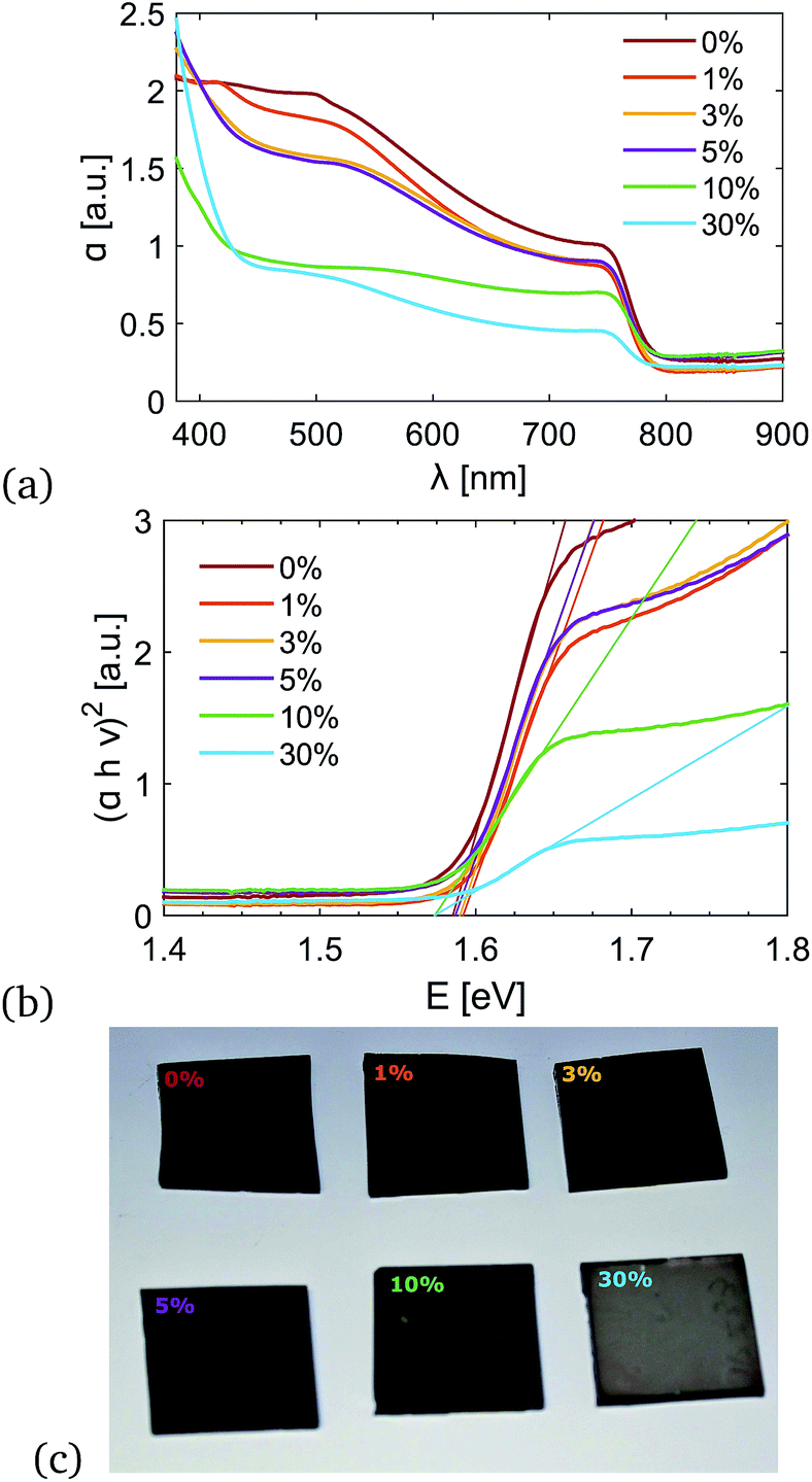 | ||
| Fig. 4 (a) UV-vis absorption spectra and (b) Tauc plot of (TBA)n(MA)1−nPbX3 perovskite films prepared on glass substrates with n = 0 (0%), 0.01 (1%), 0.03 (3%), 0.5 (5%), 0.1 (10%), 0.3 (30%) and 1 (100%) respectively; (c) images of fabricated (TBA)n(MA)1−nPbX3 perovskite films deposited on glass substrates. | ||
In Fig. 4(c), images of the (TBA)n(MA)1−nPbX3 annealed perovskite films prepared with n = 0, 0.01, 0.03, 0.5, 0.1 and 0.3 are shown. Films with n ≤ 0.05 look fairly similar. They appear to be black and reflective. At higher concentrations of TBA (n ≥ 0.1), the color changes and the film becomes more transparent. However, this net colour change is not related to the thickness of the films, which has been measured by a profilometer and found to be consistently between 300 and 350 nm (Fig. S4†). Despite the films having the same thickness, the absorption of the TBA containing films is lower. However, SEM images, which are discussed in the next section, show that the coverage is better and fewer pinholes are observed. The absorption drops when high concentrations of TBA are added to the precursor solution; this reduction is mainly due to greater transparency, as shown in Fig. S5.† Although the films prepared with higher concentrations of TBA have higher transmittance, they could be used as semi-transparent PVs for window applications.
Morphology
Fig. 5 shows the top-view SEM images of perovskite films without and with different concentrations of TBA. Perovskite films were spin coated on identical substrates and under the same conditions to compare the different SEM images and investigate the effect that TBA has on the crystallisation.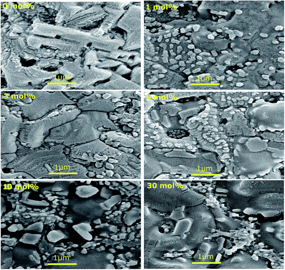 | ||
| Fig. 5 Top surface SEM images of (TBA)n(MA)1−nPbX3 perovskite films with different TBA concentrations (n = 0 (0%), 0.01 (1%), 0.03 (3%), 0.5 (5%), 0.1 (10%), 0.3 (30%) and 1 (100%) respectively); films were deposited onto a compact layer of TiO2. | ||
Neat MAPbX3 shows the typical branch-like perovskite grains.33 Particularly, large and elongated crystals are observed, fully consistent with what has previously been reported in the literature for MAPbI3−xCIx.5 Spin-coating the precursor solution directly onto the compact TiO2 layer results in a dewetting effect that causes poor surface coverage.34 Fig. S6† shows larger top view SEM images, and large pinholes on the substrate, which are coloured in red for easier comparison, are emphasized. When TBA is used, the elongated crystals disappear and larger more homogeneous crystallites with enhanced surface perovskite coverage and fewer pinholes were observed. Moreover, the SEM images show that some small crystals start to form on the surface of the film, which may be 2D TBA crystallites. When using more TBA, the number of small 2D TBA crystallites sitting on top of the perovskite grains increases. Top surface AFM images (a) without and (b–f) with TBA as the additive are illustrated in Fig. S7.† Neat MAPbX3 film crystals look quite homogeneous, with grains of similar size. When TBA is used, a much larger variety of grain sizes can be seen, with interconnected big crystals and relatively small crystals. As shown in Fig. S7(g),† the addition of TBA changes the average roughness of the perovskite films. These values have been measured over 50 μm × 50 μm size images (Fig. S8†) and averaged over 8 different images. The average roughness indicates the microscopic peaks and valleys that can be found on the surface, which is found to increase with TBA concentration.
Recent reports have suggested that additives, such as 2-aminoethanethiol and 2-pyridylthiourea, might slow down crystallisation, allowing the formation of intermediate phases and pushing additives from grain boundaries throughout the film to the surface of the film itself.25,26 It is possible that a similar process is also occurring when TBA is added, leading to a high concentration of 2D TBA crystallites on the surface. Looking at the colour change during annealing, it was noticed that when the TBA cation was added to the precursor solution, the reaction between the organic iodide and the PbI2 was retarded. This delay may cause enhanced surface coverage. From Fig. S6† it can be seen that at the highest TBA concentrations, 2D TBA crystallites are found in between the larger perovskite grains. In the top-view SEM of 30 mol% in Fig. 5, it can be clearly seen that some TBA crystallites are found between crystal grains and some of them can be seen underneath, suggesting a mixed 2D/3D structure.
JV performance
To investigate the photovoltaic performance, J–V curves of PSCs with and without TBA were measured and are shown in Fig. 6(a). The curves were obtained under reverse scan, the forward scan is shown in Fig. S9.† The average device performance of each case has been used as the basis of the comparison. The corresponding VOC, JSC, fill factor (FF) and power conversion efficiency (PCE) at reverse and forward voltage scans are summarized in Table 3, together with the champion PCEs obtained. It is important to note that the cells were not optimised for efficiency as it was more important to obtain a reproducible baseline for a standard cell so the effect of TBA could be understood. The efficiency can be pushed to higher values by controlling the crystallization kinetics of perovskites. Several techniques can be used, including anti-solvent methods where solvents, such as toluene or chlorobenzene, are dripped onto the spinning perovskite to obtain smooth and compact films.35 However, it was not clear whether the anti-solvent method would change the ratio of 2D to 3D perovskite in the cells with TBA so it was decided to use the simplest preparation method and to sacrifice some efficiency for better comparability.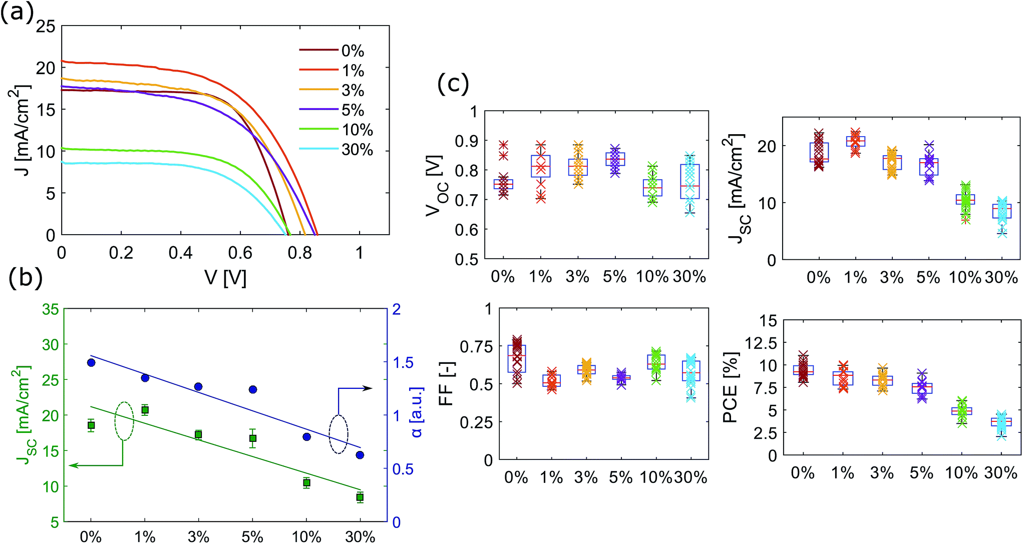 | ||
| Fig. 6 (a) JV curves of average performing devices based on 3D MAPI perovskites (0%) and mixed 2D/3D (TBA)n(MA)1−nPbX3 (with n = 0 (0%), 0.01 (1%), 0.03 (3%), 0.5 (5%), 0.1 (10%), 0.3 (30%) and 1 (100%) respectively). Typical JV curve obtained by reverse scan from 1.2 V to 0 V. (b) JSC and average spectral absorption of films (absorption data averaged between 450 and 750 nm) as a function of the concentration of TBA; the error bars indicate upper and lower 95% confidence interval boundaries computed for a normal distribution fitted to the dataset (between 11 and 21 different pixels for each TBA concentration). (c) Photovoltaic parameters shown as box plots for efficiency distributions of perovskite solar cells based on 3D and mixed 2D/3D with various TBA concentrations tested under AM 1.5 and 1 sun illumination (reproducibility evaluated by characterising between 11 and 21 different pixels for each TBA concentration). | ||
| Concentration of TBA | Dir. | V OC [V] | J SC [mA cm−2] | FF | PCE [%] | ch. PCE [%] |
|---|---|---|---|---|---|---|
| 0% | rev. | 0.75 | 17.46 | 0.68 | 8.87 | 11.05 |
| for. | 0.75 | 16.95 | 0.62 | 7.88 | ||
| 1% | rev. | 0.85 | 20.82 | 0.56 | 9.91 | 9.95 |
| for. | 0.84 | 20.71 | 0.51 | 8.76 | ||
| 3% | rev. | 0.81 | 18.71 | 0.58 | 8.85 | 9.64 |
| for. | 0.81 | 18.63 | 0.54 | 8.25 | ||
| 5% | rev. | 0.85 | 17.75 | 0.53 | 8.01 | 9.08 |
| for. | 0.85 | 17.95 | 0.49 | 7.51 | ||
| 10% | rev. | 0.76 | 10.37 | 0.61 | 4.85 | 6.03 |
| for. | 0.75 | 10.20 | 0.55 | 4.25 | ||
| 30% | rev. | 0.75 | 8.75 | 0.59 | 3.88 | 4.53 |
| for. | 0.74 | 8.58 | 0.56 | 3.55 |
According to the literature, when mixed FA/MA cells and triple cation Cs/FA/MA cells are fabricated, the hysteresis is commonly not pronounced.29,36 Similarly, the presence of large cations, such as cyclopropylammonium and polymeric ammonium, seemed to reduce the hysteresis effect with respect to standard MAPbX3 cells.12,18 It is interesting to note that in contrast to what is found in the literature, the presence of TBA does not appear to reduce hysteresis.
Final devices demonstrate good reproducibility (Fig. 6(c)). JV curves in Fig. 6(a) show that initially the average photogenerated current increases when a thin 2D perovskite layer is added (1 mol%). This could occur if the 2D perovskite layer passivates the surface of the film. However, when the amount of 2D perovskite in the film is further increased (TBA concentration higher than 3 mol%), more transparent films were obtained and the photocurrent decreased. The maximum current that can be extracted from a device strongly depends on the light absorption. The photogenerated current was found to decrease as the transparency of the perovskite films increased. JV curves as well as JSC and film transparency data are shown in Fig. 6(a) and (c). Similarly, Yao et al. observed that the JSC of mixed methylammonium and polymeric-ammonium devices was lower than the JSC of the control MAPbX3.18 It is possible that the presence of thick 2D perovskite layers reduces carrier mobility, increasing the electron–hole recombination.10 1 mol% was found to be the optimum TBA concentration to get the maximum extractable current.
The open circuit voltage is improved slightly (by an average of 0.05 V) following the addition of low concentrations of TBA. SEM images proved that higher coverage is obtained when TBA is added to the solution, decreasing the pinhole density. Further increasing the concentration of TBA pushes the VOC to lower values, comparable to the one obtained for the reference solar cell (0% TBA). On the other hand, devices with 10% and 30% of TBA showed higher FF.
The PCE decreases with the concentration of TBA; the main parameter affecting a lower PCE is the JSC. A reduction in the photocurrent was observed for higher transmittance devices, which is fully consistent with what is observed in the literature.37,38Fig. 6(b) shows the JSC and the spectral absorption as a function of the concentration of TBA in the precursor solution. It was found that the reduction of absorption with increasing concentration of TBA was mainly due to higher transparency. When compared to the trend of photocurrent, a linear correlation between optical properties and JSC was found.
Long term stability
An important advantage of the TBA containing perovskite solar cells is that we found them to have a higher resistance to moisture. Fig. 7 shows the long term stability of samples without and with 1 mol%, 3 mol% and 5 mol% of TBA added to the precursor solution.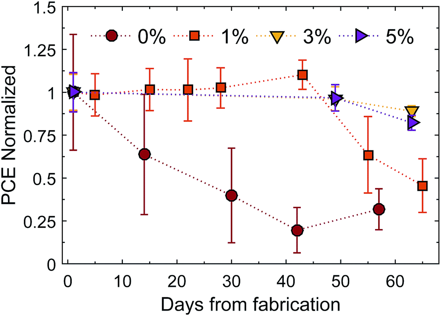 | ||
| Fig. 7 Evolution of PCE over time for samples without and with different concentrations of TBA ((TBA)n(MA)1−nPbX3 with n = 0 (0%), 0.01 (1%), 0.03 (3%), 0.5 (5%)). Each point is representative of 6 pixels. The marker indicates the mean value of each set of data. The top and the bottom of the error bars are upper and lower 95% confidence interval boundaries computed for a normal distribution fitted to the dataset. All the values have been normalised with respect to the mean value obtained after deposition (7.13%, 7.36%, 8.73% and 6.65% for 0%, 1%, 3% and 5% TBA respectively). | ||
Solar cells were stored in the dark, at room temperature and ambient relative humidity, which varied between 30% and 60% over time, and tested without encapsulation in an ambient environment. The variation of the other device parameters (VOC, JSC and FF) is shown in Fig. S11.†VOC and FF were not significantly affected by moisture. The photocurrent density of the device without TBA decreases in just a few days. On the other hand, the PCE of devices with some TBA starts to drop after about 45 days, showing much slower degradation. We believe that the bulky organic TBA delays the ingress of water, slowing the degradation of the device when stored under ambient conditions. These results reinforce the conclusion that 2D TBA crystallites are present at the surface. The perovskite structure of mixed cation films decomposed when dipped into water. However, contact angle measurements using water droplets showed that the mixed cation perovskite films had a more hydrophobic surface (see Fig. 8). This result might significantly contribute to the greater moisture stability reported.
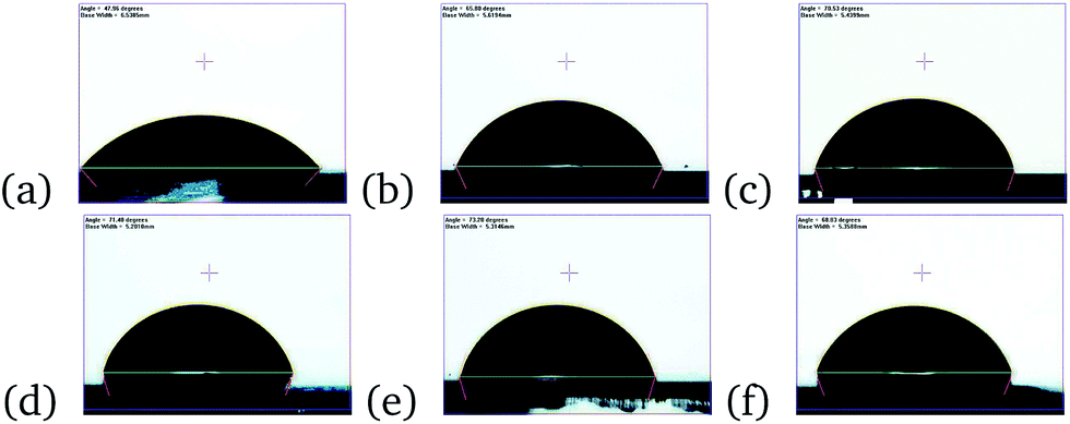 | ||
| Fig. 8 Water contact angle measurements of perovskite films (a) without and (b–f) with various concentrations of TBA added to the solution. (a) 0% TBA: 48 °C; (b) 1% TBA: 66 °C; (c) 3% TBA: 71 °C; (d) 5% TBA: 72 °C; (e) 10% TBA: 73 °C; (f) 30% TBA: 69 °C. | ||
After about 45 days the cells with TBA started losing their efficiency. However, degradation and decomposition of the solar cells might be affected by other factors, such as damage to the Au contacts due to repeated measurements, corrosion of thin metal layers,19 degradation of the spiro HTM due to hygroscopic additives39 and formation of voids in the perovskite layer due to detachment of the material from the TiO2 layer.19 Films with TBA look black after over 100 days, indicating that the formation of PbI2 may not be the main degradation mechanism (see Fig. S12†). Once water molecules attack the perovskite interface, it has been suggested that CH3NH2 and volatile gases are released, enlarging the pinholes and causing delamination, which limits charge collection.39 As water molecules gain access through pinholes, smooth and pinhole-free surfaces are expected to show higher stability.40 By optimizing the device with anti-solvent methods, the stability of mixed TBA–MA perovskite based solar cells is expected to reach greater heights.
Conclusions
In summary, (TBA)n(MA)1−nPbX3 perovskite films with improved hydrophobicity have been observed. Tetrabutylammonium was added to the perovskite precursor solution in different concentrations. The films containing TBA, which is a much larger cation than MA, showed better coverage and fewer pinholes when compared to a MAPbI3 film. The presence of TBA delayed the formation of the perovskite phase, retarding the change in film colour change. X-ray diffraction measurements showed that mixed TBA/MA films lead to the growth of perovskite films, where the 2D perovskite phase coexisted with the 3D MAPbI3 phase. Top-view SEM images suggested that 2D (TBA)PbX3 crystallites are deposited on the surface when TBA is added. 2D perovskite layers may result in surface passivation; we estimated that the maximum extractable current was obtained when a TBA concentration of 1 mol% was used. The TBA containing perovskite solar cells showed higher moisture stability, with stable PCE after more than 40 days under ambient conditions without encapsulation. We suggest that TBA cations might be driven to the surface of perovskite grains. The bulky alkyl chains could act as a hydrophobic layer on the surface, delaying the degradation of the perovskite film under ambient conditions.Conflicts of interest
There are no conflicts to declare.Acknowledgements
We acknowledge Mrs Ursula Potter for her assistance in SEM acquisition. We would like to thank the EPSRC Centre for Doctoral Training in Sustainable Chemical Technologies (EP/L016354/1). This project has received funding from the European Union's Horizon 2020 research and innovation programme H2020-MSCA-CO-FUND-2014 (# 665992, MSCA FIRE: Fellows with Industrial Research Enhancement). Dataset available – see DOI: https://doi.org/10.15125/BATH-00403.References
- M. M. Lee, J. Teuscher, T. Miyasaka, T. N. Murakami and H. J. Snaith, Science, 2012, 338, 643–647 CrossRef CAS PubMed.
- H.-S. Kim, C.-R. Lee, J.-H. Im, K.-B. Lee, T. Moehl, A. Marchioro, S.-J. Moon, R. Humphry-Baker, J.-H. Yum, J. E. Moser, M. Grätzel and N.-G. Park, Sci. Rep., 2012, 2, 591 CrossRef PubMed.
- M. A. Green, K. Emery, Y. Hishikawa, W. Warta, E. D. Dunlop, D. H. Levi and A. W. Y. Ho-Baillie, Prog. Photovoltaics, 2017, 3–13 Search PubMed.
- M. a. Green, A. Ho-Baillie and H. J. Snaith, Nat. Photonics, 2014, 8, 506–514 CrossRef CAS.
- S. T. Williams, F. Zuo, C. C. Chueh, C. Y. Liao, P. W. Liang and A. K. Y. Jen, ACS Nano, 2014, 8, 10640–10654 CrossRef CAS PubMed.
- C.-c. Chueh, C.-z. Li and A. K. Jen, Energy Environ. Sci., 2015, 1–30 Search PubMed.
- W. Zhang, M. Saliba, D. T. Moore, S. K. Pathak, M. T. Horantner, T. Stergiopoulos, S. D. Stranks, G. E. Eperon, J. A. Alexander-Webber, A. Abate, A. Sadhanala, S. Yao, Y. Chen, R. H. Friend, L. A. Estroff, U. Wiesner and H. J. Snaith, Nat. Commun., 2015, 6, 6142 CrossRef CAS PubMed.
- R. G. Niemann, A. G. Kontos, D. Palles, E. I. Kamitsos, A. Kaltzoglou, F. Brivio, P. Falaras and P. J. Cameron, J. Phys. Chem. C, 2016, 120, 2509–2519 CAS.
- N. J. Jeon, J. H. Noh, Y. C. Kim, W. S. Yang, S. Ryu and S. I. Seok, Nat. Mater., 2014, 13, 1–7 Search PubMed.
- T. Leijtens, G. E. Eperon, N. K. Noel, S. N. Habisreutinger, A. Petrozza and H. J. Snaith, Adv. Energy Mater., 2015, 5, 1500963 CrossRef.
- A. M. A. Leguy, Y. Hu, M. Campoy-Quiles, M. I. Alonso, O. J. Weber, P. Azarhoosh, M. van Schilfgaarde, M. T. Weller, T. Bein, J. Nelson, P. Docampo and P. R. F. Barnes, Chem. Mater., 2015, 27, 3397–3407 CrossRef CAS.
- C. Ma, C. Leng, Y. Ji, X. Wei, K. Sun, L. Tang, J. Yang, W. Luo, C. Li, Y. Deng, S. Feng, J. Shen, S. Lu, C. Du and H. Shi, Nanoscale, 2016, 338, 643–647 Search PubMed.
- D. H. Cao, C. C. Stoumpos, O. K. Farha, J. T. Hupp and M. G. Kanatzidis, J. Am. Chem. Soc., 2015, 137, 7843–7850 CrossRef CAS PubMed.
- D. H. Cao, C. C. Stoumpos, T. Yokoyama, J. L. Logsdon, T.-B. Song, O. K. Farha, M. R. Wasielewski, J. T. Hupp and M. G. Kanatzidis, ACS Energy Lett., 2017, 2, 982–990 CrossRef.
- H. Tsai, W. Nie, J.-C. Blancon, C. C. Stoumpos, R. Asadpour, B. Harutyunyan, A. J. Neukirch, R. Verduzco, J. J. Crochet, S. Tretiak, L. Pedesseau, J. Even, M. A. Alam, G. Gupta, J. Lou, P. M. Ajayan, M. J. Bedzyk, M. G. Kanatzidis and A. D. Mohite, Nature, 2016, 536, 312–316 CrossRef CAS PubMed.
- I. C. Smith, E. T. Hoke, D. Solis-Ibarra, M. D. McGehee and H. I. Karunadasa, Angew. Chem., Int. Ed., 2014, 53, 11232–11235 CrossRef CAS PubMed.
- G. Grancini, I. Zimmermann, E. Mosconi, D. Martineau and S. Narbey, Nat. Commun., 2017, 1–8 Search PubMed.
- K. Yao, X. Wang, F. Li and L. Zhou, Chem. Commun., 2015, 51, 15430–15433 RSC.
- Y. Han, S. Meyer, Y. Dkhissi, K. Weber, J. M. Pringle, U. Bach, L. Spiccia and Y.-B. Cheng, J. Mater. Chem. A, 2015, 3, 8139–8147 CAS.
- T. Salim, S. Sun, Y. Abe, A. Krishna, A. C. Grimsdale and Y. M. Lam, J. Mater. Chem. A, 2015, 3, 8943–8969 CAS.
- S. N. Habisreutinger, T. Leijtens, G. E. Eperon, S. D. Stranks, R. J. Nicholas and H. J. Snaith, Nano Lett., 2014, 14, 5561–5568 CrossRef CAS PubMed.
- F. Bella, G. Griffini, J.-P. Correa-Baena, G. Saracco, M. Grätzel, A. Hagfeldt, S. Turri and C. Gerbaldi, Science, 2016, 4046 Search PubMed.
- T. Miyasaka, B. Chaudhary, A. Kulkarni, A. K. Jena, M. Ikegami, Y. Udagawa, H. Kunugita and K. Ema, ChemSusChem, 2017, 1–8 Search PubMed.
- S. Yang, Y. Wang, P. Liu, Y.-B. Cheng, H. J. Zhao and H. G. Yang, Nat. Energy, 2016, 1, 1–7 Search PubMed.
- B. Li, C. Fei, K. Zheng, X. Qu, T. Pullerits, G. Cao and J. Tian, J. Mater. Chem. A, 2016, 17018–17024 CAS.
- M. Sun, F. Zhang, H. Liu, X. Li, Y. Xiao and S. Wang, J. Mater. Chem. A, 2017, 5, 13448–13456 CAS.
- S. Eslava, J. Urrutia, A. N. Busaworv, M. R. Baklanov, F. Iacopi, S. Aldea, K. Maex, J. A. Martens and C. E. A. Kirschhock, J. Am. Chem. Soc., 2008, 130, 17528–17536 CrossRef CAS PubMed.
- C. Sun, Q. Xue, Z. Hu, Z. Chen, F. Huang, H. L. Yip and Y. Cao, Small, 2015, 11, 3344–3350 CrossRef CAS PubMed.
- M. Saliba, T. Matsui, J.-Y. Seo, K. Domanski, J.-P. Correa-Baena, M. K. Nazeeruddin, S. M. Zakeeruddin, W. Tress, A. Abate, A. Hagfeldt and M. Grätzel, Energy Environ. Sci., 2016, 9, 1989–1997 CAS.
- J. S. Banait, K. S. Sidhu and J. S. Walia, Can. J. Chem., 1984, 62, 303–305 CrossRef CAS.
- T. Baikie, Y. Fang, J. M. Kadro, M. Schreyer, F. Wei, S. G. Mhaisalkar, M. Graetzel and T. J. White, J. Mater. Chem. A, 2013, 1, 5628 CAS.
- K. Sun, J. Chang, F. H. Isikgor, P. Li and J. Ouyang, Nanoscale, 2015, 7, 896–900 RSC.
- Y. Zhao and K. Zhu, J. Phys. Chem. C, 2014, 118, 9412–9418 CAS.
- S. D. Stranks, P. K. Nayak, W. Zhang, T. Stergiopoulos and H. J. Snaith, Angew. Chem., Int. Ed., 2015, 54, 3240–3248 CrossRef CAS PubMed.
- J. Seo, J. H. Noh and S. I. Seok, Acc. Chem. Res., 2016, 49, 562–572 CrossRef CAS PubMed.
- D. Bi, W. Tress, M. I. Dar, P. Gao, L. Jingshan, C. Renevier, K. Schenk, A. Abate, F. Giordano, J.-P. Correa-Baena, J.-D. Decoppet, S. M. Zakeeruddin, M. K. Nazeeruddin, M. Gratzel and A. Hagfeldt, Sci. Adv., 2016, 2, 1–7 Search PubMed.
- G. E. Eperon, V. M. Burlakov, A. Goriely and H. J. Snaith, ACS Nano, 2014, 8, 591–598 CrossRef CAS PubMed.
- P. You, Z. Liu, Q. Tai, S. Liu and F. Yan, Adv. Mater., 2015, 27, 3632–3638 CrossRef CAS PubMed.
- I. Lee, J. H. Yun, H. J. Son and T.-S. Kim, ACS Appl. Mater. Interfaces, 2017, 9(8), 7029–7035 CAS.
- F. Wu and L. Zhu, Sol. Energy Mater. Sol. Cells, 2017, 167, 1–6 CrossRef CAS.
Footnote |
| † Electronic supplementary information (ESI) available. See DOI: 10.1039/c7ta06735f |
| This journal is © The Royal Society of Chemistry 2017 |