
 Open Access Article
 This Open Access Article is licensed under a
 Creative Commons Attribution 3.0 Unported Licence
How reliable are efficiency measurements of perovskite solar cells? The first inter-comparison, between two accredited and eight non-accredited laboratories†
Ricky B.
Dunbar
 *a,
Benjamin C.
Duck
a,
Tom
Moriarty
b,
Kenrick F.
Anderson
a,
Noel W.
Duffy
c,
Christopher J.
Fell
a,
Jincheol
Kim
d,
Anita
Ho-Baillie
d,
Doojin
Vak
e,
The
Duong
f,
YiLiang
Wu
f,
Klaus
Weber
f,
Alex
Pascoe
g,
Yi-Bing
Cheng
g,
Qianqian
Lin
h,
Paul L.
Burn
h,
Ripon
Bhattacharjee
i,
Hongxia
Wang
i and
Gregory J.
Wilson
a
*a,
Benjamin C.
Duck
a,
Tom
Moriarty
b,
Kenrick F.
Anderson
a,
Noel W.
Duffy
c,
Christopher J.
Fell
a,
Jincheol
Kim
d,
Anita
Ho-Baillie
d,
Doojin
Vak
e,
The
Duong
f,
YiLiang
Wu
f,
Klaus
Weber
f,
Alex
Pascoe
g,
Yi-Bing
Cheng
g,
Qianqian
Lin
h,
Paul L.
Burn
h,
Ripon
Bhattacharjee
i,
Hongxia
Wang
i and
Gregory J.
Wilson
a
aCSIRO Energy, Mayfield West, NSW, 2304 Australia. E-mail: greg.wilson@csiro.au
bNational Renewable Energy Laboratory, Golden, Colorado 80401, USA
cCSIRO Energy, Clayton, VIC, 3800 Australia
dAustralian Centre for Advanced Photovoltaics (ACAP), School of Photovoltaic and Renewable Energy Engineering, University of New South Wales, Sydney 2052, Australia
eCSIRO Manufacturing, Bag 10 Clayton South, Victoria 3168, Australia
fResearch School of Engineering, The Australian National University, Canberra, ACT 2601, Australia
gDepartment of Materials Science and Engineering, Monash University, Clayton, VIC 3168, Australia
hCentre for Organic Photonics & Electronics, School of Chemistry and Molecular Biosciences, The University of Queensland, QLD, 4072 Australia
iSchool of Chemistry, Physics and Mechanical Engineering, Science and Engineering Faculty, Queensland University of Technology, Brisbane, Australia
First published on 24th October 2017
Abstract
Perovskite materials have generated significant interest from academia and industry as a potential component in next-generation, high-efficiency, low-cost, photovoltaic (PV) devices. The record efficiency reported for perovskite solar cells has risen rapidly, and is now more than 22%. However, due to their complex dynamic behaviour, the process of measuring the efficiency of perovskite solar cells appears to be much more complicated than for other technologies. It has long been acknowledged that this is likely to greatly reduce the reliability of reported efficiency measurements, but the quantitative extent to which this occurs has not been determined. To investigate this, we conduct the first major inter-comparison of this PV technology. The participants included two labs accredited for PV performance measurement (CSIRO and NREL) and eight PV research laboratories. We find that the inter-laboratory measurement variability can be almost ten times larger for a slowly responding perovskite cell than for a control silicon cell. We show that for such a cell, the choice of measurement method, far more so than measurement hardware, is the single-greatest cause for this undesirably large variability. We provide recommendations for identifying the most appropriate method for a given cell, depending on its stabilisation and degradation behaviour. The results of this study suggest that identifying a consensus technique for accurate and meaningful efficiency measurements of perovskite solar cells will lead to an immediate improvement in reliability. This, in turn, should assist device researchers to correctly evaluate promising new materials and fabrication methods, and further boost the development of this technology.
Introduction
Since the first demonstration in 2009![[thin space (1/6-em)]](https://www.rsc.org/images/entities/char_2009.gif) 1 of solar cells using a semi-conductor from a class of materials known as metal-halide perovskites, perovskite solar cells have been the subject of intense investigation as candidate materials to drive further growth in the photovoltaics (PV) industry. While the majority of the development so far has centred on opaque single junction devices, other potential applications, such as tandem solar cells and semi-transparent transparent devices, also hold great potential.
1 of solar cells using a semi-conductor from a class of materials known as metal-halide perovskites, perovskite solar cells have been the subject of intense investigation as candidate materials to drive further growth in the photovoltaics (PV) industry. While the majority of the development so far has centred on opaque single junction devices, other potential applications, such as tandem solar cells and semi-transparent transparent devices, also hold great potential.
A primary reason for the strong interest in perovskite-based solar cells is the high efficiency—the ratio of the maximum device power output divided by the input power—reported for research prototype cells. The highest independently confirmed efficiency for single-junction cells is 22.1%,2 which was achieved for a device with an area of 0.0946 cm2. For a somewhat larger device (0.9917 cm2) the record certified efficiency is 19.7%, which is relatively close to other established PV technologies such as CIGS or CdTe (both 21.0% for a comparable cell size). This improvement in efficiency of prototype-scale devices, to reach values comparable with existing commercial technologies in only seven years, has been remarkable. Recently demonstrated devices that utilise mixed-cation, two-dimensional and mixed-halide perovskites appear to exhibit particularly promising device performance3–5 and stability.5,6 Furthermore, interfacial engineering has also been intensively investigated and efficient devices have been reported based on novel transport materials, such as poly(triaryl amine) (PTAA),4 BaSnO37 and CuGaO2.8
However, there are considerable difficulties associated with reliable measurement of the efficiency of perovskite solar cells that are a serious concern for device research and development and even raise doubt about past reports of world record devices.9 Although the measurement procedures published in international standards10 are highly effective for “well-behaved” devices, such as most wafer-based silicon solar cells, these standards presently lack sufficient direction to address the complex challenges presented by perovskite solar cells.
As a consequence, the research community has been forced to develop various ad hoc approaches to measuring device efficiency for perovskite solar cells. This immediately raises the question as to whether some approaches are more reliable than others. The lack of a reliable method for measuring cell efficiency is a major issue, since the efficiency metric is almost universally used to guide device development and optimisation. If the true performance is not being correctly measured, there is a risk that promising fabrication techniques are not identified, and conversely, that inferior techniques are pursued instead.
Therefore, a standardised approach to the measurement of efficiency that can deliver a reliable assessment of cell performance is urgently needed. In particular, such an approach also needs to produce measurement results that are relevant for field application.
In this work, we quantify the impact of the present lack of standardised performance assessment techniques by carrying out the first inter-laboratory comparison of perovskite solar cells. While there are an increasing number of device architectures and fabrication methods reported in the literature, the underlying mechanisms that cause significant measurement issues have not fundamentally changed in nature.11 We address these measurement issues in a holistic manner by considering the influence of commonly used measurement techniques on two devices with significantly different response characteristics. The results are applicable to devices with varying response times and in particular, these results can still be applied to newer materials with more favourable transient properties. The findings of the inter-comparison allow us to quantify the measurement variability between laboratories that arise due to the unique, complex behaviour of perovskite devices. We then propose methodologies that may help reduce inter-laboratory variability in the future, and identify techniques which are suitable for high accuracy measurements, regardless of device type.
Background
Before we introduce the complex challenge of efficiency measurement for perovskite solar cells, we will first describe the methodology for performance assessment for PV devices in general.As PV devices are sensitive to operating conditions, such as irradiance, device temperature, solar spectrum and angle of incidence, the PV community has adopted a convention of reporting device performance at fixed conditions, known as the standard test conditions (STC), to enable fair comparisons between devices. The standard conditions specify a device temperature of 25 °C and a fixed spectral irradiance, known as AM 1.5G, with a total irradiance of 1000 W m−2 and a spectral distribution derived from a model of natural sunlight. Performance measurements at approximately STC can be performed with relatively simple equipment, however, higher accuracy measurements require specialised equipment and expertise. Where the highest accuracy is required, such as independently verifying breakthrough device performance, the community relies on recognised test centres that are externally accredited for technical competency according to international standards (IEC 60904-1 and ASTM E948).
A central metric used by researchers to quantify PV performance at STC is the current–voltage characteristic, or I–V curve. This curve expresses the electrical current, and by extension, the power, that can be generated as a function of the potential difference (voltage) across the device electrodes. The range of voltage values included in the characteristic varies, but always includes values spanning the region between open-circuit (OC), where zero current flows, and short-circuit (SC), where zero potential difference exists across the device. Several important performance parameters can be obtained from I–V curves, in particular, the voltage and current at which the maximum power can be produced by the solar cell, referred to as the maximum power point (MPP). The power conversion efficiency, or simply, the efficiency, is the ratio of the output power at MPP divided by the input power (solar irradiance). Knowledge of the I–V curve can also provide valuable information on the physical mechanisms governing power generation and is important for control systems for deployed devices.
An I–V curve is typically measured by varying (scanning) the voltage across the device and recording the measured current at each voltage. Typically, I–V curves are performed in a step-wise fashion, maintaining each voltage for a finite time – referred to as the dwell time – prior to measuring the current and then abruptly changing to the next voltage. For “well-behaved” PV devices, it can generally be assumed that the device current rapidly stabilises (on a sub-millisecond timescale) to a value based only on the existing measurement conditions (voltage, temperature and spectral irradiance) and not on the prior history of the device. For this reason, I–V scans are commonly carried out with short dwell times, yielding entire I–V curves within milliseconds (in pulsed illumination systems) to seconds (continuous illumination).
However, the situation is more complex for some PV technologies, for which modified measurement techniques have been developed. For example, dye-sensitised solar cells, which typically exhibit longer response times (millisecond to second timescale) to changes in bias, can require I–V sweep times of 5 s or more (corresponding to a scan rate of less than 150 mV s−1) to allow sufficient current stabilisation at each bias value.12,13 The three most commercially established thin-film PV technologies – copper indium gallium selenide (CIGS), cadmium telluride (CdTe) and amorphous silicon (a:Si) – can typically be measured with rapid I–V scans (including pulsed), but require careful stabilisation treatments prior to measurement, referred to as pre-conditioning. This pre-conditioning is required because these devices can exhibit long-term (much longer than the time required for a single measurement) meta-stable behaviour. Although no international standard for thin-film device performance assessment exists, the standard for qualification of thin-film modules (IEC 61646) requires that modules are exposed to a minimum of two 43 kWh m−2 light soaking cycles. A recent study by Kenny et al. found that this treatment yields repeatable performance measurements for CIGS (although only when I–V curves where measured immediately following light-soaking), whereas at least five cycles were required to fully stabilise CdTe modules, and even nine cycles were insufficient to achieve stabilisation in a:Si/μ:Si modules.14 High efficiency and high capacitance crystalline silicon modules generally do not require pre-conditioning, but their response time can require sweep times of greater than 100 ms (sweep rate less than 7500 mV s−1) to ensure the current at each voltage stabilises prior to measurement.15 This is typically problematic for conventional pulsed I–V measurement systems, many of which have a flash duration of around 10 ms. For these devices, testing with long pulse flash illumination or even continuous illumination can be required.
Efforts up until now to achieve repeatable measurements of efficiency for perovskite solar cell at STC tend to indicate that, at least for present research prototype devices, the challenges faced for perovskite solar cells are greater than for other PV cell types. These difficulties, which have been widely discussed,16–22 are a due to a complex, dynamic device response to changes in cell voltage (during I–V scans) and test conditions, in particular, the change from ambient conditions to STC. The timescales of key dynamic processes span a particularly large range—from nanoseconds23 through to seconds, minutes and even hours.22 As expected, when I–V measurements are performed on these devices on comparable timescales, the extent of stabilisation at each voltage value is highly dependent on the chosen scan rate, as well as on the previous history of the device. Furthermore, this has also been observed to be strongly dependent on film morphology24 and device architecture.16
The fact that measurement results exhibit a significant dependence on the technique, device history,20,22 and device architecture is clearly undesirable. An obvious solution to this problem would be simply to perform slower scans, allowing sufficient time for complete stabilisation at each voltage value. This however, is only feasible if the device does not undergo irreversible performance degradation during the measurement. For perovskite solar cells, it generally cannot be assumed that this is the case – see the recent review on stability by Leijtens et al.25
Thus, a critical question for perovskite solar cell research is how to perform accurate, repeatable and meaningful efficiency measurements. Some authors have offered suggestions on best-practice measurement techniques,21,26,27 including measuring I–V curves in both (increasing and decreasing) voltage scan directions and at various scan rates, supplementing these measurements with additional techniques. However, there is still much work to be done towards arriving at one or more prescriptive standard approaches that achieve consensus amongst PV researchers. In particular, methods are required to be general enough to address the varying transient properties observed for different cell architectures. A key requirement is that the measured performance is not affected by transient processes, rather, that it represents the stabilised or steady-state performance of the device. For I–V curves, it follows that the current at each voltage value must be steady-state to yield the steady-state voltage dependence.
Below, we briefly describe approaches that have been used to measure the efficiency of perovskite solar cells.
Measurement techniques
The latter three techniques described above all permit dynamic measurement times to ensure stabilisation, and differ primarily in the measurement output (MPP, a single I–V pair and a full I–V curve, respectively). In fact, one could consider the dynamic I–V approach to simply be a set of consecutive SCFV measurements at voltage values to cover the range of interest. An advantage of dynamic approaches is that they inherently incorporate pre-conditioning by allowing sufficient time for stabilisation prior to the measurement. These flexible approaches are well-suited to address systems where required stabilisation times are a complex function of multiple variables.22 In contrast, conventional I–V curves require careful consideration of pre-conditioning treatments and scan parameters. This can be difficult to establish and may result in measurements that are either longer than necessary, leading to the risk of measurement error due to degradation, or not long enough, resulting in non-steady-state measurements. Prior to this work, a dynamic approach, using pre-defined stability criteria has been implemented by Dunbar et al.22 for perovskite devices for steady-state measurements of short-circuit current density (Jsc) and open-circuit voltage (Voc). Some authors have monitored stabilisation at each voltage in step-wise I–V curves without setting the times dynamically.18,19 The SCFV approach has been widely used16 and MPPT has been used by some authors.28
Experimental
The inter-comparison was carried out between April and October 2016 between CSIRO's PV Performance Laboratory (hereafter referred to simply as CSIRO), NREL and eight Australian PV research laboratories. The two independent test laboratory participants, CSIRO and NREL, hold accreditation to the ISO/IEC 17025 technical competency standard for performance measurements for PV cells, and used their typical equipment and test procedures in the inter-comparison. The participating research laboratories were, in a randomised order: the University of New South Wales, Australian National University, Monash University, University of Queensland, Queensland University of Technology, two CSIRO PV research groups in Melbourne and Newcastle (both of which are physically and operationally separate from CSIRO's accredited PV Performance Laboratory) and one additional laboratory, the name of which is undisclosed due to reasons of commercial confidentiality. As the purpose of this study was to assess the role of measurement technique, and not to identify which institutes have reliable measurement procedures and which do not, results for the research laboratory participants are presented anonymously. The eight research laboratories were assigned alphabetic identifiers according to the chronological order of the measurements from A (first) to G (last).To enable monitoring of any device degradation, a star-type inter-comparison was chosen, where the host laboratory (CSIRO) measured the circulated devices periodically throughout the study. All participant results were reported to, and collated by, CSIRO. The inter-comparison device set included two packaged perovskite solar cells and one packaged KG1-filtered silicon control device.
There were two key requirements for the selection of suitable perovskite samples for this study. The first was that they exhibited a favourable combination of efficiency and stability for devices of their size (the chosen cells had a nominal area of 1 cm2). This requirement was necessary to enable an effective comparison of measurement results between multiple institutes over an extended period of time. The second was that the cells exhibited considerably different behaviour during efficiency measurement. This requirement was imposed to enable an assessment of the effectiveness of common techniques for devices of varying dynamic behaviour, in particular, to identify which techniques were most effective regardless of the device under test.
The perovskite cells, identified as ‘A’ and ‘B’, were contributed by an external laboratory in response to a request from the host laboratory for samples that met these requirements. The host laboratory was not informed of, and thus did not disclose to the participants, the respective architecture of the devices until the completion of the study. It was subsequently revealed that cell A, which exhibited generally slower transient behaviour, was fabricated with a triple-layer scaffold of meso-TiO2|ZrO2|C infiltrated by a perovskite semi-conductor, similar to that fabricated by Mei et al.29 Cell B, which exhibited generally faster transient behaviour, was fabricated with a c-TiO2|meso-TiO2|perovskite|C architecture, similar to that fabricated by Zhou et al.30 The perovskite compound used in both devices was CH3NH3PbI3 (MAPbI3). The influence of the choice of these configurations of perovskite compound and architecture on the results of this study is discussed later in this paper.
The cells were sealed with a polymer gasket and a glass cover slip and supplied to CSIRO with two wires attached to each electrode respectively for electrical contact. At CSIRO they were then individually packaged in cast aluminium enclosures (details provided in the ESI†). Although the packages introduced optical losses and hence reduced the device efficiency, this was considered acceptable given the benefits that the packages provided. These benefits included: easy device handling and positioning in test beds, and additional protection for the devices against degradation during storage and transit. To further minimise the risk of degradation, the first phase of the inter-comparison, involving only the Australian laboratories, was carried out over a short time period (9 laboratories in 14 days). When in storage at the host laboratory, the cells were kept in the dark in a low-moisture desiccator cabinet.
The third cell in the inter-comparison set, cell C, was a commercially packaged KG1-filtered monocrystalline silicon reference cell (PV Measurements) with a nominal area of 4 cm2. Cell C served as an important control device for the study for two reasons. Firstly, as a packaged reference solar cell, it can be considered to be highly stable over the duration of the inter-comparison. Secondly, as a monocrystalline silicon cell, the complex transient behaviour observed for perovskite solar cells can be considered to be absent.
Participants were asked to perform their “best practice” measurement of the efficiency of the devices. At a minimum, they were required to include I–V parameters derived from forward (SC to OC) and reverse (OC to SC) scans but were also encouraged to try any additional technique they considered appropriate. As no information was provided on the architecture or expected device behaviour during efficiency measurement, participants were permitted to perform preliminary tests to identify the most appropriate approach to use for each cell.
Only two laboratories (CSIRO and NREL) measured the area of the devices, whereas the others assumed the nominal values. The method used to measure device area at CSIRO has been described previously.31 To enable comparison, all results have been expressed to the nominal area values. CSIRO and NREL were also the only participants to report the external quantum efficiency and correct for spectral mismatch. We compare area values and external quantum efficiency curves measured by CSIRO and NREL in the ESI (Fig. S1–S4†).
Results
Silicon control device
Measurements of six key solar cell performance metrics – open-circuit voltage (Voc), short-circuit current density (Jsc), fill-factor (FF), voltage at MPP (Vmpp), current density at MPP (Jmpp) and efficiency – reported by inter-comparison participants for the silicon control device are shown in Fig. 1. The results reported by Lab E for this cell deviate significantly from the other results – for reasons that will be discussed shortly – and are omitted from Fig. 1 for clarity, but the entire set of results is presented in Fig. S5 in the ESI.† The periodic host laboratory measurements (squares) are in mutual agreement to within the indicated error bars (expressed to a confidence level of approximately 95%), as expected due to the high stability of the reference cell. Results from the two laboratories that hold accreditation for PV measurement, CSIRO and NREL (triangles), are also in good agreement.§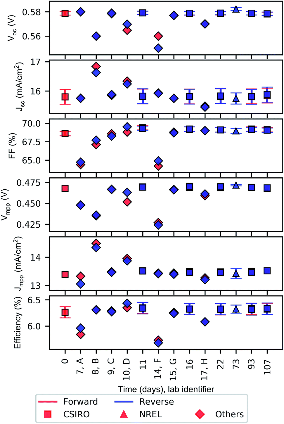 | ||
| Fig. 1 Inter-comparison results for cell C: a KG1-filtered packaged monocrystalline silicon reference cell. Where reported by participants, uncertainty levels are indicated by error bars expressed to a confidence level of approximately 95%. | ||
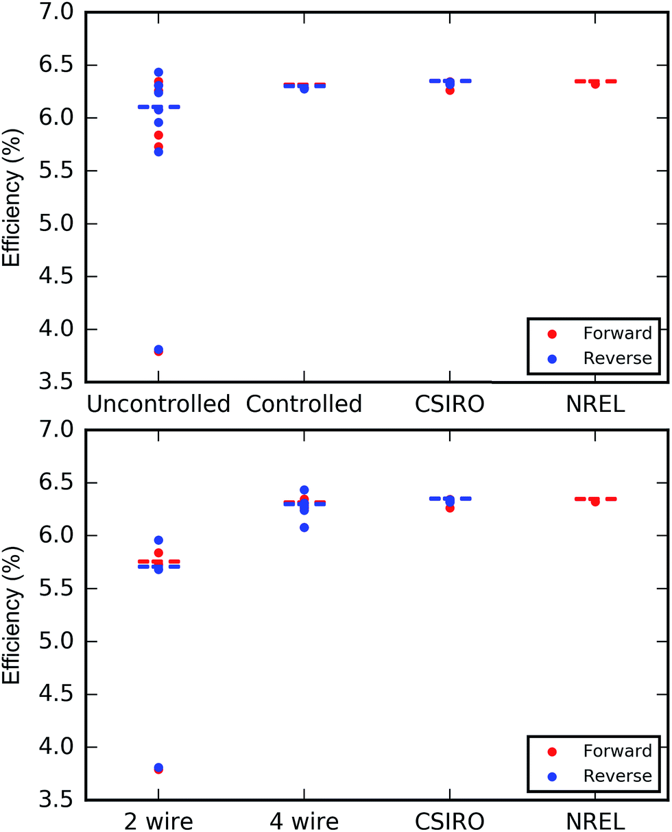
The results reported by the other participants (diamonds) are distributed about the NREL and CSIRO values with varying agreement, which we now attempt to explain based on the measurement technique employed by each participant. The IEC 60904-1 and ASTM E948 standards for PV performance assessment describe measurement procedures which the PV research community uses, to varying degrees of adherence, for efficiency measurements. In Table 1, the adherence of the inter-comparison participants to key good measurement practices within the standard methodology are listed. We identify the most important practices as those, which, when absent, are associated with the largest discrepancies from the results reported by CSIRO and NREL, which followed all practices. From this it follows that the most important practice for this device is using a 4-wire electrical connection, followed by controlling the temperature of the cell to the desired test temperature. The effect of the absence of these practices is shown in Fig. 2. Labs using 2-wire measurements generally reported lower efficiency values. This is expected, as unlike 4-wire connections, a 2-wire connection fails to eliminate the series resistance, R, of the measurement circuit from the I–V curve. The consequence is that for each current value, I, in the I–V curve, the measured voltage is reduced by a voltage drop of IR across the measurement circuit. This voltage drop for each current value in the I–V curve results in an overall reduction in the measured device fill-factor and, hence, efficiency. While this error may not be significant for small-area/low current devices, the use of a 4-wire connection is evidently important for this 4 cm2 filtered silicon reference cell. Laboratory E, which used a two-wire connection, reported a particularly low efficiency. There were two other labs that used two-wire connections, and while they also reported significantly lower FF than all other participants, it is likely the effect was mitigated somewhat compared to Lab E by using lower resistance test leads. Labs that didn't control the cell temperature also reported lower values. Assuming a negative temperature coefficient, typical for silicon solar cells, this observation can be attributed to measurements being performed at temperatures higher than 25 °C, due to, for instance, cell heating during multiple measurements or device alignment under illumination. Excluding Lab E, the inter-laboratory variability expressed to two standard deviations between the non-accredited participants is 2.8 (3.6)% for Voc, 5.2 (4.4)% for Jsc, 5.8 (5.4)% for FF and 7.4 (7.6)% for efficiency as derived from scans in the forward (reverse) direction.
| Measurement practice | CSIRO | NREL | LAB | LAB B | LAB C | LAB D | LAB E | LAB F | LAB G | LAB H |
|---|---|---|---|---|---|---|---|---|---|---|
| Cell temp. controlled | Y | Y | N | N | Y | N | N | N | N | N |
| Cell temp. monitored | Y | Y | N | N | Y | Y | Y | N | N | Y |
| Environment temp. monitored | Y | Y | N | N | Y | Y | N | N | N | Y |
| Light source referenced | Y | Y | Y | Y | Y | Y | Y | N | Y | Y |
| DUT height considered | Y | Y | Y | Y | Y | N | Y | N | Y | Y |
| DUT lateral position considered | Y | Y | Y | Y | Y | Y | Y | Y | N | N |
| 4-Wire electrical contact | Y | Y | N | Y | Y | Y | N | N | Y | Y |
 | ||
| Fig. 2 Two measurement practices were particularly decisive in the measured efficiency for the silicon cell (cell C): the use of a 4-wire electrical connection (bottom) and temperature control of the device (top). Horizontal, dashed lines show the median values for each category. | ||
In Table 2, we compare the variability of the reported short-circuit current (where each value is expressed as the average of the values obtained from forward and reverse scans) to previously reported round-robin results for packaged silicon cells. The results of this study are found to lie within the range of previous inter-comparison results.
| Participants | Samples | I sc variation (2σ) (mean variation of all samples) | Ref. | |
|---|---|---|---|---|
| a Calculated (by the authors of this paper) from data provided in reference. b This result was calculated using a single CSIRO measurement which was performed on day 22: between the completion of measurements by the Australian labs and prior to the NREL measurement. | ||||
| 1986 | The top PV research labs in 8 countries – perhaps the equivalent of what are now accredited test labs | 14 crystalline silicon cells; 2 cm × 2 cm in size; identically packaged behind a quartz window with temperature control | 5.6%a | 32 |
| 1989 | A second round-robin of the key international PV labs – now 9 countries, all recognised as having high end measurement capabilities | Two packaged CZ cells, two packaged multicrystalline cells and one packaged FZ cell | 1.54% | 33 |
| 1993 | Third international round robin – 13 laboratories in 8 countries. Three results were removed because they were not ‘primary’ calibrations | 20 crystalline silicon cells; 2 cm × 2 cm in size; identically packaged behind a quartz window with temperature control (WPVS package) | 7.3%, then results were heavily filtered to achieve 1.9% for establishment of WPVS | 34 |
| 2017 | Four labs (three non-accredited + AIST) | 4 crystalline silicon cells; 2 cm × 2 cm in size; identically packaged behind a quartz window with temperature control (WPVS package) | 0.8%a | 35 |
| 2017 | (i) 8 non-accredited PV research labs in Australia | 1× packaged mono:Si cell (2 × 2 cm, KG1 filter) | (i) 4.8% | This paper |
| (ii) 8 non-accredited PV research labs in Australia + CSIROb and NREL | (ii) 4.4% | |||
Perovskite devices: host measurements
Before we present the inter-comparison results for the perovskite devices, we will describe the approach taken by the host laboratory (CSIRO) to identify appropriate measurement procedures for each cell.Fig. 3 shows the transient behaviour during a trial pre-conditioning treatment at STC with the device held at open-circuit. Device temperature was controlled with a thermoelectric stage, with temperature setpoints chosen so that the stabilised cell temperature was close to 25 °C. This simple test illustrates the different dynamic behaviours of the two perovskite devices (A and B) and the silicon cell (C). The Voc was monitored for 45 minutes, or until stabilisation to a pre-defined criterion occurred. This criterion, which mandated an absolute rate of change of less than 0.025%/min evaluated over the most recent 4 minutes of data, was determined in previous work.22 Whereas the transient behaviour in cell C can be attributed to the increase in temperature that occurs when the shutter is opened (as evident by the linear Voc–T relationship to which the dataset conforms, see inset), the transient response of the perovskite solar cells are slower and more complex. Both perovskite cells exhibit an initial increase in Voc reaching a maximum after approximately 1 and 10 minutes for cells B and A, respectively, followed by a gradual decrease towards the stabilised value. For cell B, the Voc stabilises within 20 minutes, but the Voc for cell A does not meet the stability criterion within the monitoring period. The shape of the purple curve in the inset suggests that for cell B, the transient response to the change in illumination dominates in the first minutes of the measurement, after which the Voc appears to be primarily governed by the device temperature. In contrast, the transient response for cell A persists well after the temperature has stabilised. We note that the absolute temperature change for perovskite solar cells is greater than for the silicon cell due to the thermal properties of the packages being different, resulting in larger differences between the in temperature between the device and the stage.
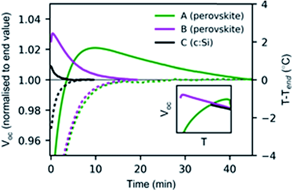 | ||
| Fig. 3 Transient behaviour exhibited by the inter-comparison devices following a transition from ambient room light to full illumination. The open-circuit voltage (full lines) and device temperature (dashed lines) are continuously measured until stabilisation occurs (see text). The inset plot shows the same Voc data, plotted as a function of T. These measurements were performed at CSIRO. | ||
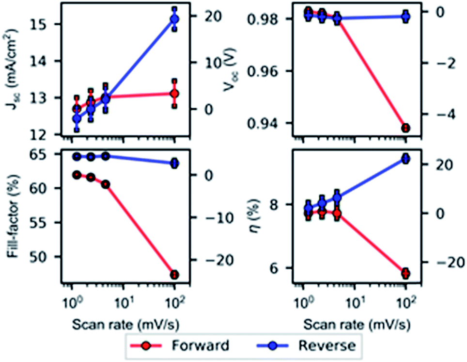
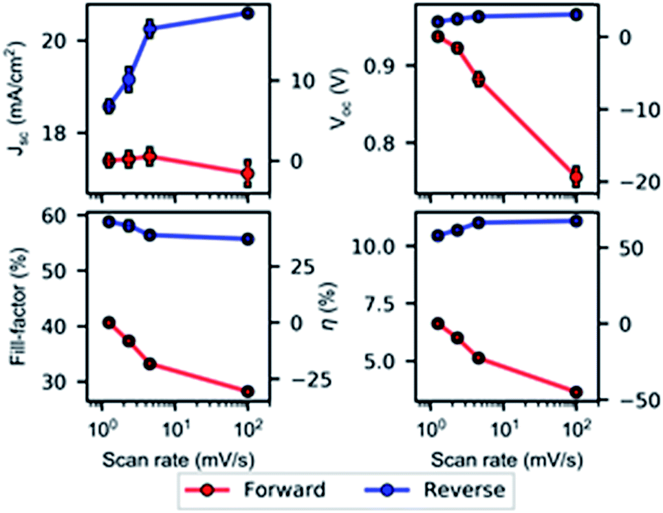
The results in Fig. 3 reveal information on the transient response of the perovskite cells to two kinds of change in conditions: a change in the irradiance (from room light level to near one sun) and a change in cell temperature. A third important change in conditions is the change in voltage bias, as occurs during all I–V scans. To identify suitable I–V scan parameters for the perovskite cells A and B, an investigation of the influence of scan rate on the I–V behaviour was performed. The exact pre-conditioning and measurement sequence is described in the ESI.† We note that to minimise the risk of degradation during investigations prior to the inter-comparison, we limited the investigation to the influence of the scan rate only. The pre-conditioning procedure was chosen based on previous studies.20,22 The scans were performed step-wise with a fixed step of 50 mV and variable dwell times at each voltage equivalent to scan rates of 100, 4.5, 2.3 and 1.3 mV s−1. The scan rates were trialled in decreasing order.
Fig. 4 and 5 show key I–V parameters as a function of scan rate for cells B and A, respectively. We observe a high degree of repeatability (good agreement between two repeat measurements) for each combination of scan direction and rate. For both cells, we observe that the pre-conditioning is sufficient to achieve reasonable stabilisation at the scan starting voltage (i.e. 0 V for the forward scans, Voc for the reverse scans), as demonstrated by a relatively small variation of these parameters with scan rate. In contrast, the I–V parameter measured at the end of the scan (Voc for the forward scan and Jsc for the reverse scan) are under- and over-estimated, respectively for larger scan rates. In general, all 4 parameters converge as the scan rate is reduced, suggesting that the scan parameters are approaching those required to capture steady-state current–voltage dependence.
 | ||
| Fig. 4 Identification of the most suitable scan rate for host measurements of cell B. Scans are performed in forward (SC to OC) and reverse (OC to SC) directions. Four scan rates are chosen with two repeats for each value. Squares indicate individual measurements and circles indicate the corresponding mean. Where two repeat measurements returned very similar results, the squares can be difficult to distinguish individually. The right-hand-side axis shows the difference in percent of values from the mean value of the forward scans at the slowest scan rate. | ||
 | ||
| Fig. 5 Identification of the most suitable scan rate for host measurements of cell A. See main text and caption for Fig. 4. | ||
Cell B (Fig. 4) exhibited a significant discrepancy between I–V parameters extracted from scans in the forward and reverse directions at 100 mV s−1. However, for the three slower scan rates trialled, relatively good agreement was achieved. The I–V curves from which these parameters have been extracted are shown in Fig. SI6 in the ESI.†
For cell A (Fig. 5), significant differences between scan directions are observable even at the slowest scan rate trialled, indicating that these scan rates still fail to provide the device sufficient time for the current to stabilise at each voltage. The corresponding I–V curves (Fig. 6) clearly show the widely observed overshoot in current near MPP for the reverse scans, leading to errors near MPP that reduce slowly with decreasing scan rate. In contrast, the apparent errors near SC decrease more rapidly with decreasing scan rate.
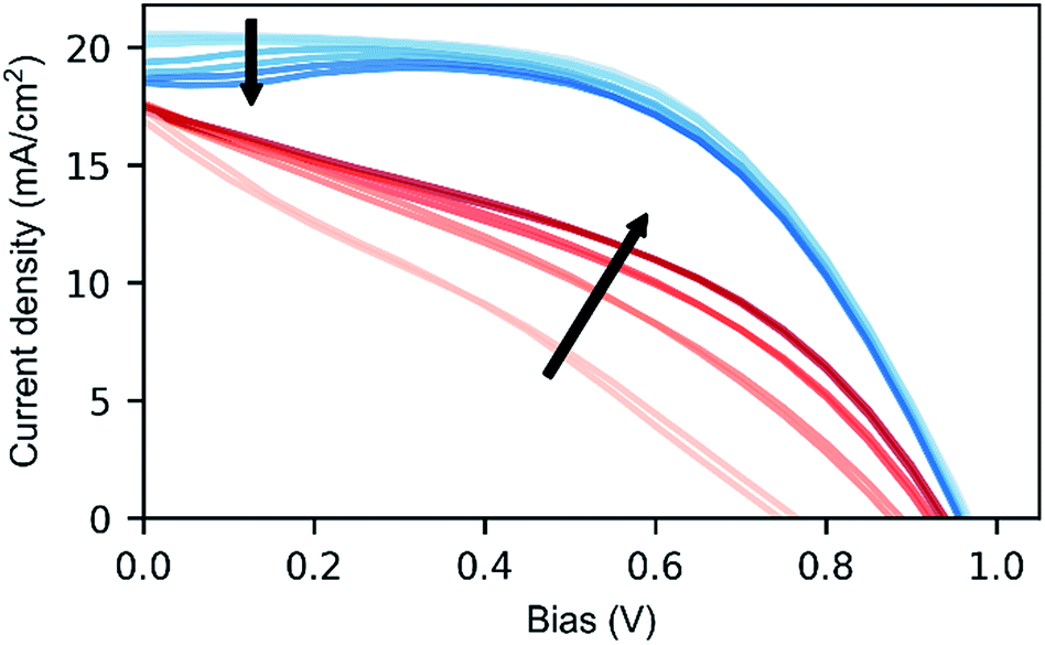 | ||
| Fig. 6 I–V scans for cell A as measured by CSIRO. Arrows indicate decreasing scan speed for each scan direction (blue/upper curves = reverse and red/lower curves = forward). | ||
It is likely that a combination of extending the duration of pre-conditioning and using slower scan speeds would have enabled steady-state behaviour to be more accurately probed for cell A. However, based on Fig. 3 and 5, it seems likely that this would require pre-conditioning and scan times on the timescale of hours. Due to concerns that doing so would increase the risk of the cell not remaining sufficiently stable throughout the inter-comparison, longer measurements were not considered.
Following the initial investigation,¶ a measurement sequence (consisting of steps 1–5 listed in Section 5 of the ESI†) using a scan speed of 2.3 mV s−1 with a step size of 50 mV, was used for both cells for all subsequent CSIRO measurements during the inter-comparison.
Perovskite devices: inter-comparison
The measurement approaches employed by all participants for perovskite devices A and B are summarised in Table 3. These parameters supplement the information on general measurement practices in Table 1.| CSIRO | NRELa | Lab A | Lab B | Lab C | Lab D | Lab E | Lab F | Lab G | Lab H | |
|---|---|---|---|---|---|---|---|---|---|---|
| a At NREL, conventional I–V measurements of perovskite cells, such as those required to be performed for this comparison (red/blue markers in Fig. 7 and 8), are automatically labelled as “bogus” they are believed inappropriate for this device type. Instead, the dynamic approach (cyan markers in Fig. 7 and 8) is preferred. b Cell held at scan start voltage. c Used previous I–V scans to estimate Vmpp to use as fixed voltage. | ||||||||||
| I–V scans | ||||||||||
| Pre-conditioning | ||||||||||
| Treatment | Start Vb | None | r. I–V | V oc | V oc | V oc | r. I–V | 0 V | r. I–V | V oc |
| Light exp. duration (s) | 600 | n/a | 60 | 120 | 600|60 | 360|120 | 600 | 300 | 264|72 | 180 |
| Exp. end condition | Time | n/a | Stable Pmax | Stable Pmax | Time | Stable Voc | Stable Pmax | Max Jsc | Stable Pmax | Time |
|
||||||||||
| Scans | ||||||||||
| Max voltage (V) | 1.0 | 1.0 | 1.1 | 1.0 | 1.05 | 1.1 | 1.1 | 1.1 | 1.2 | 1.2 |
| Min voltage (V) | 0.0 | 0.0 | −0.1 | −0.2 | −0.05 | −0.1 | −0.2 | 0 | −0.2 | −0.2 |
| No. measurement points | 21 | 50 | 100 | 101 | 100 | 120 | 120 | 65 | 100 | 70 |
| Dwell time (s) | 30 | 0.2 | 0.11 | 0.1 | 0.1 | 0.2 | 0.1 | 0.1 | 0.1 | 0.2 |
| 1st scan direction | Fwd | Rev | Rev | Fwd | Rev | Rev | Rev | Rev | Rev | Fwd |
| 2nd light exp. duration (s) | 300 | 0 | 0 | 360|120 | 300|60 | 120|60 | 204|180 | 180 | ||
| 2nd exp. end condition | Time | Stable | Stable | Stable | n/a | Stable | Stable | Max | Stable | Time |
| 2nd scan direction | Rev | Fwd | Fwd | Rev | Fwd | Fwd | Fwd | Fwd | Fwd | Rev |
|
||||||||||
| Additional measurement | ||||||||||
| Method | — | Dyn.IV | — | — | MPPT | SCFVc | SCFVc | SCFVc | — | — |
I–V parameters reported by the participants are shown in Fig. 7 and 8 for cells B and A, respectively. The same marker and colour conventions are used in Fig. 1 with the addition of cyan markers which denote dynamic measurements. We note that some dynamic measurements, such as MPPT, return only a subset of I–V parameters. Full dynamic I–V curves, such as the method employed by NREL – referred to as “Asymptotic Pmax” – acquire Jsc, Voc and the “knee” region of the IV curve containing the MPP.
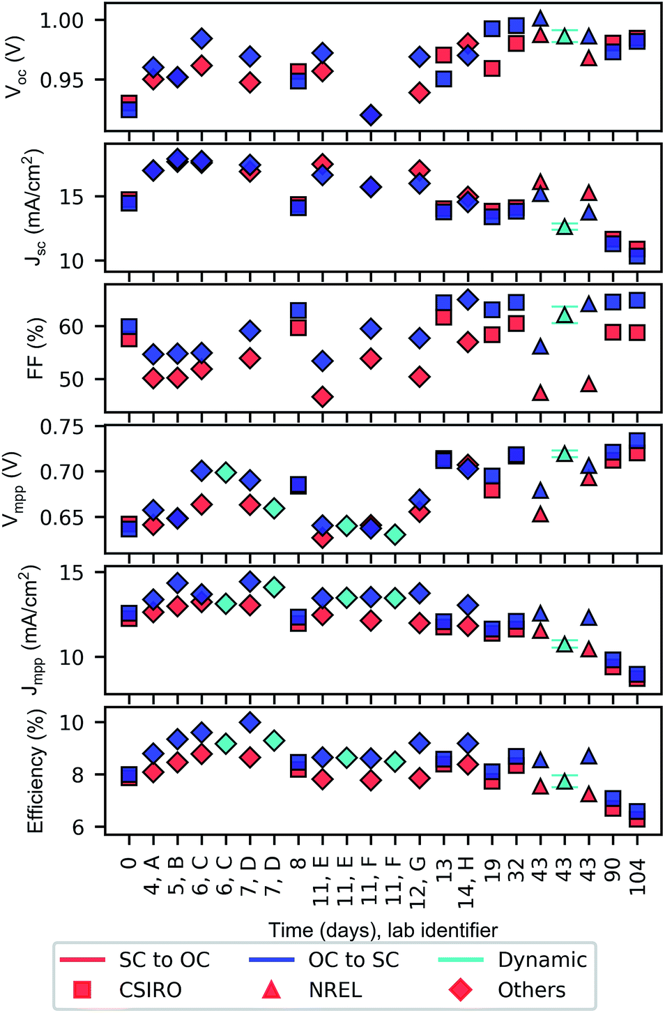 | ||
| Fig. 7 Inter-comparison results for cell B. Where reported by participants, uncertainty levels are indicated by error bars expressed to a confidence level of approximately 95%. | ||
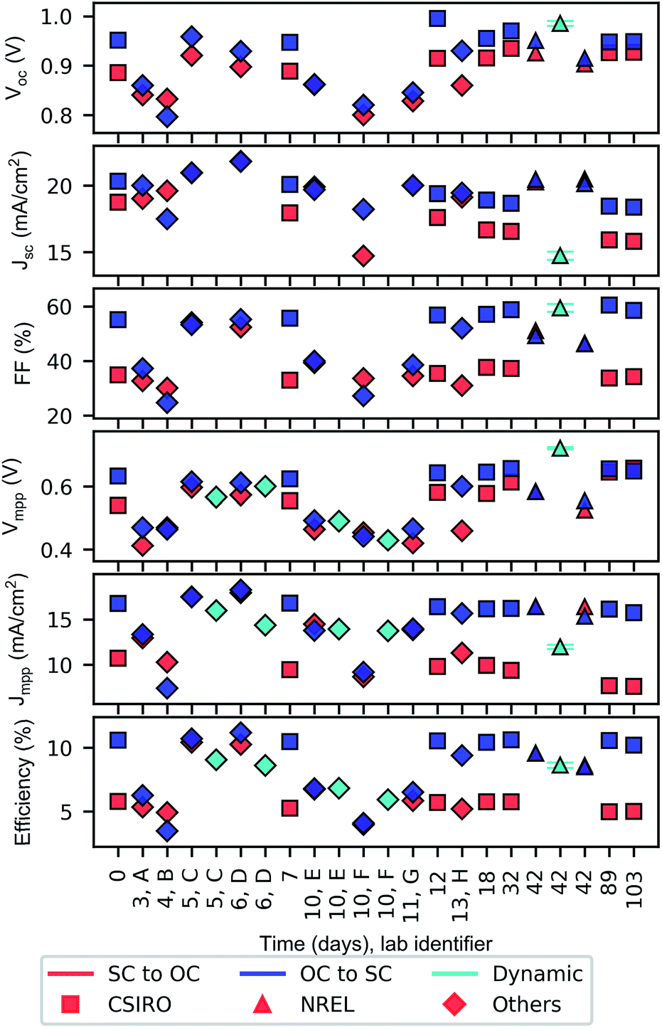 | ||
| Fig. 8 Inter-comparison results for cell A. Where reported by participants, uncertainty levels are indicated by error bars expressed to a confidence level of approximately 95%. | ||
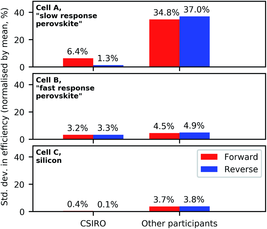
The overall variability (1σ) in reported efficiency is shown in Fig. 9 for two categories: (1) all repeat host measurements and (2) all non-accredited participants. We note that due to the anomalous result reported by Lab E for cell C due to the large series resistance introduced into the measurement, this result is omitted from this figure. Drawing our attention first to cell C in the lowest pane, we see that as expected, the variability is small (<1%) for the repeat host measurements where identical procedures were used by the same operator with the same equipment each time. The variation between the non-accredited participants is somewhat larger (3.7% and 3.8% for the forward and reverse scans, respectively) due to the variation in measurement approaches, equipment and operators as discussed at the start of the Results section.
 | ||
| Fig. 9 1σ variability observed for the repeat host measurements (left) and all non-accredited participants (right) for forward and reverse I–V measurements. The following measurements have been omitted from consideration: cell C – Lab E (anomalous FF due to 2-wire measurement); cell B – two final CSIRO measurements (days 90 and 104), as degradation had clearly occurred prior to these measurements due to international transit. | ||
For cell B, the variability of the host measurements is between 3.2 and 3.3% for both scan directions. This significant variation, which is observed despite the use of identical measurement procedures, is attributed to longer-term (timescale of days) device aging. This will be discussed in detail in the next section. For the non-accredited participants, the variation is between 4.5 and 4.9% for both scan directions. This variation is approximately 1% greater than observed for the stable reference cell (C), which, based on the corresponding host variability, must be due in part to device aging effects. However, given the observation that most labs reported significant discrepancy between I–V parameters from different scan directions, it is also likely to be partially due to the effectiveness of different measurement techniques in the presence of short-term transient processes relevant for the perovskite device.
For cell A, the variability of the host measurements is clearly larger in the forward direction (6.4%) than the reverse direction (1.3%). The reason for this difference is not completely clear, but a contributing factor is likely to be that the forward scans were always performed first, and by the time the reverse scan commenced, the additional illumination during the forward scan may have served to further pre-condition the device and hence reduced the influence of prior device history.
In comparison to the repeat host measurements, the variability between the non-accredited participants is considerably larger: 34.8 and 37.0% for the two scan directions. This result, which serves as a quantitative indication of the general measurement reliability for slowly responding perovskite cells, is one of the key results of this paper. If we compare the average of the variability in both scan directions for each cell, we find the increase in variability compared to cell C is a factor of 1.3 for cell B and 9.6 cell A. The reasons for this large variation observed for the perovskite cells, in particular for cell A, are investigated in detail in the Discussion.
Device stability
Before proceeding to the Discussion, we will briefly comment on the influence of device stability on the interpretation of the inter-comparison results. In Fig. 9, we see for cells A and C, the variation in host measurements over the study was significantly lower than the inter-comparison measurements. It follows that the stability was more than sufficient to enable to impact of variations in measurement technique (and equipment) to be clearly observed. For cell B, the host and inter-laboratory measurement variability are more similar, which makes the role of measurement approach somewhat more difficult to assess. Nevertheless, we find that we are still able to isolate the role of measurement technique (see Fig. S8 in the ESI†).The variation in host laboratory results throughout the intercomparison can be observed in Fig. 7 and 8 (square markers). The corresponding I–V curves are shown in Fig. S7.† Two explanations for the observed variation present themselves. The first is that the true steady-state performance exhibits long-term stability (invariant with device age), but the implemented device pre-conditioning is insufficient to prevent previous device history from affecting the result. The second is that the steady-state performance is not constant, but changes with device age.
For cell B, recalling that the measurement approach appears to capture steady-state behaviour to a good extent (Fig. 4), we attribute the majority of the variability to genuine changes in the device performance over time. As opposed to a gradual decrease, as would be expected if irreversible degradation dominated these changes, the performance appears to both increase and decrease, that is, until a clear sign of degradation appears. This occurs between CSIRO measurements on days 32 and 90, during which time the cell had been shipped internationally to and from NREL. The transit introduced multiple factors, including extended exposure to ambient conditions, extreme temperatures, pressure fluctuations, and mechanical shock, all of which could be expected to promote degradation. It is not known which of these influences were of most importance in causing the observed degradation.
For cell A, the reduction in efficiency during international transit was relatively minor. In contrast to cell B, the shape of the I–V curves changes throughout the inter-comparison (Fig. S7†). Particularly notable is that with age, the bump near MPP for the reverse scan becomes increasingly prominent, which is consistent with previous observations by O'Regan et al.36 This behaviour invites comparison to a similar observation made when performing I–V scans at varying scan rates at a constant device lifetime (see our Fig. 5 and 1a of Tress et al.17). The decrease in the forward short-circuit current with age (also observed by both by O'Regan et al. and Tress et al.), however, must be attributed to gradual degradation, as we are confident that the value as measured in the forward scan is steady-state.
In the next section, we investigate the relationship of measurement approach on the reported values for cell A and attempt to account for the large inter-laboratory variation.
Discussion
Influence of measurement technique
To investigate the role of measurement technique on the results reported by each laboratory, each technique was reproduced under controlled conditions at CSIRO. The implementation of these techniques was matched as closely as possible to the implementation by the roadshow participants. By holding the following factors constant: operator, measurement equipment, spectral irradiance, device age and cell temperature, we were able to isolate and examine the influence of measurement technique. These measurements were performed following the completion of the inter-comparison (day 200).Fig. 10 shows I–V curves measured using four selected techniques of interest. The techniques were: dynamic I–V (used by NREL), slow scans (CSIRO), fast scans following light-soaking at OC (“OC soak”, Labs B, C, D and H) and repeat scans (Labs A, E and F).
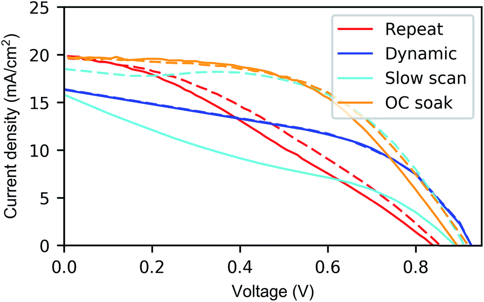 | ||
| Fig. 10 I–V curves measured at CSIRO for cell A using four techniques. Full lines indicate forward scans. Dashed lines indicate reverse scans. The OC soak and repeat scans used a scan rate of 150 mV s−1 (100-point I–V curve between −0.1 and +1.1 V). | ||
The dynamic I–V approach is considered to be the most reliable, as it allows sufficient current stabilisation at each voltage to ensure the curve reflects steady-state behaviour. In the implementation at CSIRO (Fig. 11), the current at a given fixed voltage under illumination is monitored until the rate of change becomes less than 0.2%/min, evaluated over the most recent four minutes of measurements. For this cell, the measurement of one reverse and one forward scan took over 3 hours. This corresponds to an average scan rate of 0.2 mV s−1, although we note that the scan rate is non-constant, and a measurement with a fixed scan rate of this value would be expected to be too fast for some voltage regions and too slow for others. Due to the excellent agreement between the (steady-state) I–V curves we conclude that these results were not significantly affected by degradation. The good agreement between the stabilised current measured in both directions (<1% near Vmpp and <6% for the entire curve) demonstrates that dynamic approaches can achieve accurate steady-state measurements even for slowly responding devices as long as the device is sufficiently stable. Such approaches are likely to be the most suitable for general use, from slowly responding devices similar to cell A to more rapidly responding cells similar to cell B and even cell C, provided their implementation is flexible enough. Method selection will be discussed in more detail in the Recommendations section.
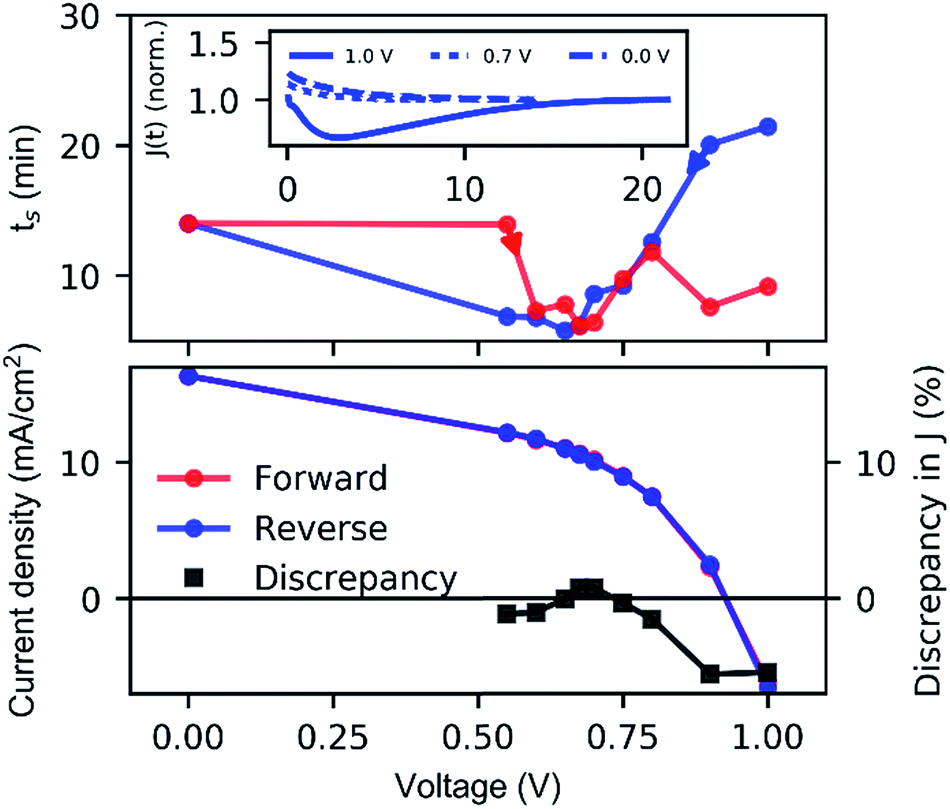 | ||
| Fig. 11 Dynamic I–V curves were measured for cell A at CSIRO, starting with the reverse scan from 1.0 to 0 V, followed immediately by the forward scan. The current at 0 V is measured only once. Top: the stabilisation time required at each voltage value for the reverse scan (blue/left arrow) and forward scan (red/right arrow). Inset: current transients (normalised to end value, time in minutes) in the reverse direction for three voltage values. Bottom: the resulting steady-state I–V curves and the discrepancy (black squares) between the forward and reverse values for each voltage. | ||
The technique that shows the second-best agreement between I–V scans in both directions in Fig. 10 is the light-soak at OC followed by consecutive fast scans (OC soak). Here, the device was held under illumination at OC for ten minutes prior to fast reverse and forward scans in immediate succession. As has been observed in the literature, the extended pre-conditioning of a device at open-circuit/forward-bias in this way can establish a device condition favourable for current generation, which, for a fast subsequent reverse scan, may be maintained to a sufficient extent such that little hysteresis is observed. It is likely that if the scan rate was increased further, even better agreement between the scan directions could have been achieved. However, as evident by comparing these curves to the dynamic I–V curves, the absence of major hysteresis isn't sufficient to claim that a measurement reflects steady-state behaviour.20 Here, the reverse and forward curves obtained using this method over-estimated the current for most of the bias voltage range below the soak voltage. This measurement approach has been referred to as “TEBBing” (temporary enhancement by bias) in the literature.36
In contrast, the approach used by CSIRO during the inter-comparison (slower scans of 2.3 mV s−1 with pre-conditioning for each scan at the start voltage) yields relatively large hysteresis. We note that even though the forward and reverse curves differ significantly, each curve is individually repeatable (Fig. 5 and 6). As was discussed earlier, the pre-conditioning at the scan start voltages ensured good stabilisation at the first voltage values of the scan, however the scan rate, which is evidently too fast to allow the current to stabilise at each voltage, returns erroneous (non-steady-state) current values for the intermediate and final voltage values (Fig. 5). The agreement between scan directions could have been improved by omitting the pre-conditioning between scans. Interestingly, as we will see in Fig. 13, the average of the efficiency values extracted by both scan directions is close to the best estimate of the steady-state value.
 | ||
| Fig. 12 Repeat scan technique results for cell A, measured at CSIRO. The two top plots show the I–V curves for the forward and reverse directions respectively. The bottom plot shows the progression of the derived efficiency as I–V curves are repeatedly measured. | ||
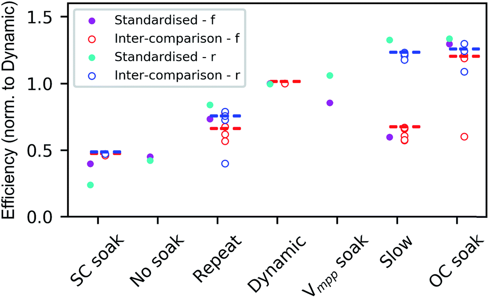 | ||
| Fig. 13 A ranking of trialled I–V measurement techniques applied to cell A, which resulted in under-estimation (left) to over-estimation (right) in the derived efficiency. f = forward and r = reverse scan directions. Each set (standardised and inter-comparison) is plotted relative to the forward dynamic result. The scan rate for the SC soak, no soak, repeat, Vmpp soak and OC soak is the same as described in the caption for Fig. 10. Horizontal lines show the median values for each category. | ||
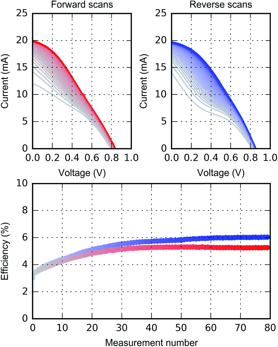
The fourth method shown in Fig. 10, which we refer to as the repeat scan technique, consists of repeatedly scanning the device in one direction until the derived efficiency stabilises. The results obtained from the implementation of this method at CSIRO are shown in Fig. 12. The sequence consisted of pre-conditioning at open-circuit under ambient room light for at least 30 minutes followed by consecutive fast scans in the same direction. For both scan directions, the performance increases sharply for the first 30 measurements, primarily due to increases in Jsc and FF, and starts to stabilise after 50–70 measurements. For the reverse scan, the characteristic bump near MPP is present for the initial scans before the I–V curves gradually become smoother. We note that although the efficiency derived from the respective scan directions does indeed stabilise, the two stabilised values are not the same, demonstrating that this technique does not yield steady-state values. We attribute the cause of this behaviour to be the constant voltage cycling, which does not permit steady-state behaviour to be reached despite the extended light-soaking. As we will see in Fig. 13, both of these stabilised values are under-estimates compared to the most reliable measurement of steady-state performance.
Fig. 13 compares the derived efficiency from all techniques reproduced at CSIRO. We will initially restrict our attention to the standardised measurements, indicated by purple and cyan dots for forward and reverse scans, respectively. The results have been arranged from left to right in order of increasing efficiency as derived from the reverse scan, and normalised relative to the forward scan of the dynamic method, which we consider to be the most reliable.
Remarkably, a difference of over 100% is observed between the results obtained with the various methods. As expected, the extended pre-conditioning at open-circuit immediately followed by a fast reverse and forward scans results in a large over-estimate, which is the largest value of any method reported in this study. The largest under-estimate is obtained by soaking the cell at short-circuit. The two non-dynamic methods which obtain the best agreement with the efficiency reported by the dynamic method are the repeat scan and the Vmpp soak.
Data from the inter-comparison are also included in Fig. 13, plotted with red and blue dots for forward and reverse scans, respectively. The trend exhibited by the inter-comparison data matches the standardised measurements at CSIRO extremely well. This confirms that for this device, the choice of I–V scan method—characterised by pre-conditioning, scan speed, scan direction and dynamic or non-dynamic scanning—is vastly more important than temperature control and irradiance calibration.|| This is in contrast to silicon cells, where the faster device response (<ms) usually means the former measurement properties are less influential, and hence the latter are of primary importance. This is compelling evidence that standardised, accurate, and reliable measurement techniques for perovskite solar cells are necessary.
The influence of the choice of inter-comparison cells
The cells used in this study were found to be very effective in enabling an exploration of the influence of measurement over a large range in device behaviour. For the faster-responding cell (B), the variability in results introduced by different measurement techniques was not significantly greater than the variability due to device aging. In contrast, for the slower-responding cell (A), the choice of measurement technique was the single most important factor in the observed results. Cells A and B were overall highly effective samples for the purposes of (i) examining the role of dynamic behaviour on inter-laboratory agreement and (ii) identifying robust techniques that are effective regardless of device composition. The samples were particularly suitable for these purposes due to the large range of response time spanned by the cells (see, for instance, Fig. 3). An added benefit of cells A and B was the use of MAPbI3, for which an extensive body of literature on ion migration, device hysteresis and light soaking effects is available.37,38 The hole transport layer-free device structures with carbon electrodes29 present in cells A and B, is not as widely investigated in the literature, but can be considered to have been of significant benefit for the stability of the devices. Nevertheless, future inter-comparisons that explore other configurations would be of great value to the research community, and we hope these results serve as a useful baseline for such future studies.Fig. 13 and S8† clearly show that the result of the application of most techniques should be expected to be highly dependent on the cell dynamics and hence on the device's specific perovskite compound and architecture. However, correctly implemented dynamic approaches can be expected to be accurate for any given perovskite solar cell, as they can return steady-state I–V curves regardless of the specifics of the transient behaviour such the form (mono-, bi-exponential or otherwise) and overall stabilisation time of current transients. Further information on this is provided in the Recommendations section. Improvements in the robustness of stabilisation criteria beyond the linear rate-of-change tolerance22 used by CSIRO in this study are likely to improve the method's versatility further, but this is beyond the scope of this study.
We note that cells A and B were selected as devices with the most favourable combination of stability and efficiency available to the host laboratory at the time when this inter-comparison was organised in early 2016. We expect that when a similar inter-comparison is carried out in the future, when higher-stability devices are available, further improvements in understanding the effect of measurement technique will be possible, and the use of faster-responding devices may improve inter-laboratory agreement. Within the literature, there is a large number of different architectures presented that combine different electrodes, electron and hole transport materials, and varying configurations of cations, anions and halides to construct the perovskite layer. Previous reports indicate that faster-responding devices, which tend to exhibit less severe hysteresis under typical measurement sequences, can be fabricated via including fabricating perovskite films with larger grains,39 reducing defect density40,41 and the use of favourable charge transport layers.
A consensus is slowly being developed that the transient behaviour of these devices is most significantly affected by an interplay between the interface trap density and the mobile ion concentration within the perovskite film.11,42 Although these processes occur entirely within the perovskite film, the dynamics are significantly influenced by interfacial properties, which is consistent with observations that the electron transport layer (ETL) and hole transport layer (HTL) both significantly affect the prevalence of hysteresis during device measurements.40,43,44 Reducing the availability of recombination centres at the perovskite/charge selective interface has been shown to decrease the magnitude of hysteresis in I–V curve measurements.
Recently the move away from MAPbI3 to materials including multiple cations including Cs and Rb has yielded improvements in stability of the perovskite crystal structure.28,45,46 The increase in perovskite film quality and stability acts to reduce the incidence and mobility of ions within the film which also acts to diminish the magnitude of observed hysteresis.
Going forward, as the quality of the perovskite layer and the quality of the interface improves, it can be expected that less interaction between mobile ions and interface states will result in further reductions of the hysteresis induced through measurement practices, as observed in recent high efficiency devices. More complex architectures may however lead to unintended consequences and different transient mechanisms such as the phase instability or segregation problem.47,48 Future work will involve the study of devices with mixed perovskite as absorbers and surface/interface passivation layers.
Recommendations
The challenge of identifying the appropriate measurement technique for a given perovskite cell is common to both research and independent laboratories. In this final section we provide recommendations on selecting a measurement technique appropriate for a given device.Required attributes for techniques
Given the complex dynamic behaviour observed for perovskite solar cells, it is instructive to remind ourselves of the objective of indoor performance assessment of PV devices. Although not explicitly stated in the present international standard,10 it is reasonable to infer that the objective is not just to determine device performance at a given temperature and spectral irradiance, e.g. at STC, but also to ensure that the measured response is that which one would observe in an actual application of the device at those conditions i.e. the field stabilised, or steady-state, performance. Thus, the MPP as measured indoors should be as what would be obtained in the field under stable, or at least slowly changing conditions, and not be affected by transient processes associated with the measurement. This applies not just to the MPP. All points on an I–V curve should be field-stabilised.It is also necessary to make a distinction between short-term metastability relevant to the timescale of a measurement (see Fig. 3) and long-term transient processes that take place over significantly larger timescales such as Staebler–Wronski degradation in a:Si and seasonal annealing. In this work, we have restricted our attention to short-term processes, and have thus adopted the definition of “steady-state” in reference to short-term processes only.
Specific considerations for standardised I–V techniques
Of all the I–V methods shown in Fig. 13, the only one that inherently quantitatively verifies steady-state behaviour is the dynamic approach. Therefore, if no restrictions on measurement time are imposed, this must be considered to be the most reliable method for slowly-responding devices.The situation becomes more complex in the presence of degradation. In such a case a compromise between two competing requirements must be made. The first requirement, which typically acts to extend the duration of a measurement, is that the measurement technique must capture the steady-state behaviour such that true voltage-dependence is not confused with reversible transient effects. The second requirement, which typically acts to reduce the duration of a measurement, is that the voltage-dependence is not confused with irreversible degradation.
To obtain the most accurate measurement of the measurand – the stabilised output in the absence of degradation – the stabilisation and degradation dynamic behaviour need to be understood to determine the optimum duration of exposure to test conditions (pre-conditioning) prior to the final, reported measurement.
A simple demonstrative case is presented in Fig. 14, where we consider a “fresh” device that has not undergone previous pre-conditioning or exposure to test conditions. To begin, we restrict our attention to the measurement of current at a fixed voltage near Vmpp. We will extend the discussion to an entire I–V curve afterwards. We represent the J(Vfixed) transient following the onset of exposure to testing conditions as a simple product of an increasing exponential term (slow approach to steady-state) and a decreasing exponential term (degradation). By choosing the respective time constants and coefficients appropriately, transient curves can be constructed for five distinct device classes: (i) ideal (immediate stabilisation and zero degradation); (ii) immediate stabilisation and moderate rate degradation; (iii) moderate rate of stabilisation and zero degradation; (iv) moderate rates of stabilisation and degradation; (v) moderate rate of stabilisation and fast rate of degradation.
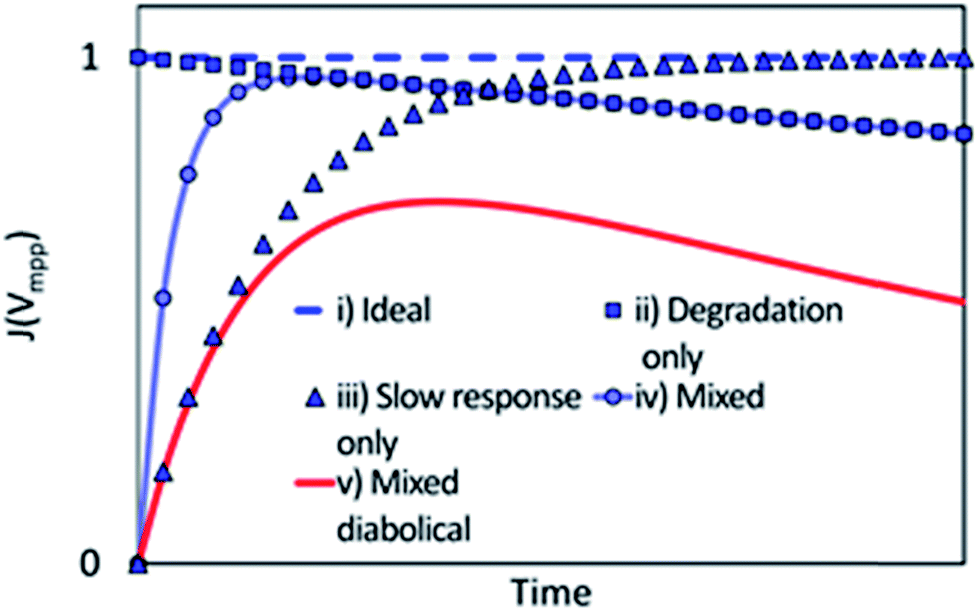 | ||
| Fig. 14 Schematic current transient, at a fixed voltage near Vmpp, arising from various contributions of degradation and slow responding processes. Transients for five device classes are shown, indicated by markers/line styles. Plot colours qualitatively indicate the magnitude of the measurement error, E (see main text and Fig. 15). | ||
Each class demands the measurement to be made within certain ranges of time from the onset of testing. Clearly, device (i) can be measured with high accuracy at any point in time. Devices (ii) and (iii) can also be measured accurately, providing, for (ii) that no practical barriers exist to measuring sufficiently quickly, and for (iii) that no practical barriers exist for sufficiently long pre-conditioning. An accurate measurement of device (v) would be difficult or impossible. Device (iv), the intermediate class, can be measured with moderate accuracy if pre-conditioning of an optimum duration (depending on stabilisation and degradation behaviour) is performed. We now propose a general framework for determining an appropriate measurement approach for a general device type.
We define parameters that provide an indicative measure of the timescale of stabilisation and degradation:
• ts, the timescale of the metastable response to changes in conditions. Following a cell perturbation from the dark state at open-circuit to STC at near Vmpp, ts is the time required for the current to reach within X% of the final steady-state value in the absence of degradation.
• td, the timescale of degradation. Time taken for steady-state value to irreversibly degrade by X% under constant exposure to testing conditions. This parameter may be easiest to estimate once metastable processes have completed.
Here, X is the measurement uncertainty, which includes all contributions present for conventional PV (we refer the reader to a previous report by Emery49 for an introduction to these contributions). An additional contribution (error), E, due to incomplete stabilisation and/or degradation, which we will discuss in general terms below, has a magnitude that depends on the device's transient properties, and once calculated, can be combined with X to obtain the total uncertainty.
The highest measurement accuracy (lowest E) is obtained when ts < td. If ts ≪ td, time will be available for multiple sufficiently pre-conditioned measurements, such as required to construct a full I–V curve. When ts and td are of a similar magnitude, the respective values can dictate the type of measurement and the resulting accuracy. For example, if X = 1%, and we determine ts and td to be 20 and 80 s, respectively, then it is likely that multiple I–V points can be measured using the SCFV method, sufficient to make a good estimate of the MPP. However, if we were to determine ts and td to both be 20 s, then it is likely that only one I–V point can be reliably measured, which will result in a less reliable efficiency measurement that is strongly reliant on a good estimate of Vmpp to use as the fixed voltage.
Fig. 15 illustrates how the respective values of ts and td can be used to determine the appropriate measurement techniques and to identify the magnitude of the error, E, that can be expected. The error due to incomplete stabilisation and/or degradation is indicated by colour, with red, white and blue indicating large, intermediate and small errors, respectively.
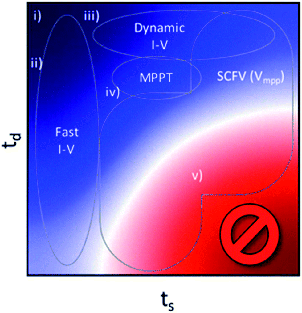 | ||
| Fig. 15 Schematic chart indicating recommended general measurement approaches for devices subject to degradation and extended stabilisation. The colour scale indicates the measurement error, E, associated with incomplete stabilisation and/or degradation for a device with a given combination of ts (indicative stabilisation time) and td (indicative degradation time). Red, white and blue indicate large, intermediate and small errors, respectively. The approaches are: fast I–V curves, maximum-power-point tracking (MPPT), stabilised current at fixed voltage (SCFV) and dynamic I–V. The location on this chart of the five demonstrative device classes shown in Fig. 14 are indicated with labels (i)–(v). | ||
Small ts
For this regime, fast I–V curves are always preferred, as they can capture the entire steady-state I–V dependence in a short amount of time, which is preferred not only for reasons of convenience and throughput, but also because faster measurements can achieve higher accuracy by minimising cell heating and the influence of long-term fluctuations in irradiance and temperature. The speed must be increased as td decreases.Moderate ts
In this regime, fast I–V scans are no longer appropriate, and techniques which permit pre-conditioning prior to measurement (SCFV, MPPT and dynamic I–V) are required. If td is large, full I–V scans (using dynamic I–V) may be possible. If td is moderate, it will only be possible to measure a limited number of I–V points using either dynamic I–V with coarse voltage spacing, or MPPT/SCFV, which only return the MPP.Large ts
In this regime, extended pre-conditioning is required to achieve stabilisation. MPPT is usually not appropriate in this regime unless the routine functions in a way similar to SCFV or dynamic I–V i.e. allowing sufficient time for stabilisation at a fixed voltage before perturbation. For extremely large ts, it is likely impractical to measure entire I–V curves, and hence measuring a limited number of I–V points near MPP using SCFV may be preferred. High accuracy can only be achieved if td is also large. For moderate td, only a limited number of I–V points near MPP using SCFV can be measured. If td is small, an accurate measurement of the steady-state behaviour is unlikely to be possible.We note that degradation and metastable processes are usually more complex than the demonstrative cases shown in Fig. 14. In particular, degradation characteristics of perovskite solar cells should not necessarily be assumed to be independent of voltage. Moreover, the stabilisation at the first voltage value after initial exposure to irradiance typically takes significantly more time than a small subsequent change in voltage without interrupting the irradiance (see the relationship between step size, order in measurement sequence and stabilisation time in Fig. 11).
Therefore, we emphasise that this framework needs to be implemented appropriately to accommodate for the specific behaviour of the devices in question.
It is also not inconceivable the trade-off discussed above can be circumvented somewhat by reducing the time required to capture steady-state behaviour. For measurements of high-efficiency silicon cells, favourably chosen voltage temporal profiles which temporarily over- or under-bias the cell can make stabilisation more rapid.50 Applied to slowly responding perovskite solar cells, this could potentially decrease the time required for efficiency measurements, and in doing so, considerably improve the accuracy.
Conclusions
This study has quantitatively demonstrated that the complex dynamic behaviour of perovskites can lead to a reduced confidence in the reliability of an efficiency measurement. By performing an inter-laboratory comparison between 8 research laboratories and two independent laboratories that hold accreditation for PV cell performance measurements (CSIRO and NREL), we are able to report the inter-laboratory agreement in efficiency measurements for a slowly-responding perovskite cell, a faster responding perovskite cell, and a control silicon cell. It is found, due to the additional complexities of efficiency measurement of perovskite cells, that the inter-laboratory variability for the faster responding perovskite cell was 1.3 times larger than for the silicon cell. For the more slowly responding perovskite cell, the variability was almost 10 times larger. We find that it was the choice of efficiency measurement method rather than temperature control or equipment calibration that was primarily responsible for this large variability. We identify the most reliable I–V technique to be the dynamic approach, followed by light-soaking at near Vmpp and the repeat I–V method. We then propose a framework that can be used to identify the most appropriate technique for a cell with a given stabilisation and degradation behaviour. We are confident that the recommendations we present based on these results, if followed, will lead to important improvements in the reliability of efficiency measurements of perovskite solar cells. This, in turn, will be highly beneficial for the correct identification of potential new materials and fabrication processes that could further accelerate the development of perovskite solar cells.Conflicts of interest
There are no conflicts to declare.Acknowledgements
This work has received funding from the Australian Renewable Energy Agency (ARENA) as part of ARENA's Emerging Renewables Program via grant P159394. This project has also been supported by the Australian Centre for Advanced Photovoltaics.Notes and references
- A. Kojima, K. Teshima, Y. Shirai and T. Miyasaka, J. Am. Chem. Soc., 2009, 131, 6050–6051 CrossRef CAS PubMed.
- M. A. Green, K. Emery, Y. Hishikawa, W. Warta, E. D. Dunlop, D. H. Levi and A. W. Y. Ho-Baillie, Prog. Photovoltaics Res. Appl., 2017, 25, 3–13 CrossRef.
- W. S. Yang, B.-W. Park, E. H. Jung, N. J. Jeon, Y. C. Kim, D. U. Lee, S. S. Shin, J. Seo, E. K. Kim, J. H. Noh and S. Il Seok, Science, 2017, 356, 1376–1379 CrossRef CAS PubMed.
- M. Stolterfoht, C. M. Wolff, Y. Amir, A. Paulke, L. Perdigón-Toro, P. Caprioglio and D. Neher, Energy Environ. Sci., 2017, 10, 1530–1539 CAS.
- G. Grancini, C. Roldán-Carmona, I. Zimmermann, E. Mosconi, X. Lee, D. Martineau, S. Narbey, F. Oswald, F. De Angelis, M. Graetzel and M. K. Nazeeruddin, Nat. Commun., 2017, 8, 15684 CrossRef CAS PubMed.
- Z. Wang, D. P. McMeekin, N. Sakai, S. van Reenen, K. Wojciechowski, J. B. Patel, M. B. Johnston and H. J. Snaith, Adv. Mater., 2017, 29, 1604186 CrossRef PubMed.
- S. S. Shin, E. J. Yeom, W. S. Yang, S. Hur, M. G. Kim, J. Im, J. Seo, J. H. Noh and S. Il Seok, Science, 2017, 356, 167–171 CrossRef CAS PubMed.
- H. Zhang, H. Wang, W. Chen and A. K. Y. Jen, Adv. Mater., 2017, 29, 1–8 Search PubMed.
- M. Gunther, Meteoric rise of perovskite solar cells under scrutiny, https://www.chemistryworld.com/news/meteoric-rise-of-perovskite-solar-cells-under-scrutiny-over-efficiencies/8324.article, accessed 28 June 2017.
- International Electrotechnical Commission 60904-1, Measurement of photovoltaic current–voltage characteristics, 2nd edn, 2006 Search PubMed.
- A. Pockett, G. E. Eperon, N. Sakai, H. J. Snaith, L. M. Peter and P. J. Cameron, Phys. Chem. Chem. Phys., 2017, 19, 5959–5970 RSC.
- G. Bardizza, D. Pavanello, R. Galleano, T. Sample and H. Müllejans, Sol. Energy Mater. Sol. Cells, 2017, 160, 418–424 CrossRef CAS.
- Y. Hishikawa, M. Yanagida and N. Koide, in 31st Photovoltaic Specialists Conference, 2005, pp. 67–70 Search PubMed.
- R. P. Kenny, A. I. Chatzipanagi and T. Sample, Prog. Photovoltaics Res. Appl., 2014, 2, 166–172 CrossRef.
- Y. Hishikawa, H. Shimura and H. Tobita, in 28th European Photovoltaic Solar Energy Conference and Exhibition, 2013, pp. 3159–3162 Search PubMed.
- H. J. Snaith, A. Abate, J. M. Ball, G. E. Eperon, T. Leijtens, N. K. Noel, S. D. Stranks, J. T.-W. Wang, K. Wojciechowski and W. Zhang, J. Phys. Chem. Lett., 2014, 5, 1511–1515 CrossRef CAS PubMed.
- W. Tress, N. Marinova, T. Moehl, S. M. Zakeeruddin, M. K. Nazeeruddin and M. Grätzel, Energy Environ. Sci., 2015, 8, 995–1004 CAS.
- E. L. Unger, E. T. Hoke, C. D. Bailie, W. H. Nguyen, A. R. Bowring, T. Heumuller, M. G. Christoforo and M. D. McGehee, Energy Environ. Sci., 2014, 7, 3690–3698 CAS.
- M. Christoforo, E. Hoke, M. McGehee and E. Unger, Photonics, 2015, 2, 1101–1115 CrossRef CAS.
- R. B. Dunbar, T. W. Jones, K. F. Anderson, G. J. Wilson and C. J. Fell, in 31st European Photovoltaic Solar Energy Conference and Exhibition, 2015, pp. 1077–1079 Search PubMed.
- Y. Hishikawa, H. Shimura, T. Ueda, A. Sasaki and Y. Ishii, Curr. Appl. Phys., 2016, 16, 898–904 CrossRef.
- R. B. Dunbar, W. Moustafa, A. R. Pascoe, T. W. Jones, K. F. Anderson, Y. B. Cheng, C. J. Fell and G. J. Wilson, Prog. Photovoltaics Res. Appl., 2017, 25, 533–544 CrossRef CAS.
- S. D. Stranks, G. E. Eperon, G. Grancini, C. Menelaou, M. J. P. Alcocer, T. Leijtens, L. M. Herz, A. Petrozza and H. J. Snaith, Science, 2013, 342, 341–344 CrossRef CAS PubMed.
- N. Mohammadian, A. Moshaii, A. Alizadeh, S. Gharibzadeh and R. Mohammadpour, J. Phys. Chem. Lett., 2016, 7, 4614–4621 CrossRef CAS PubMed.
- T. Leijtens, G. E. Eperon, N. K. Noel, S. N. Habisreutinger, A. Petrozza and H. J. Snaith, Adv. Energy Mater., 2015, 5, 1–23 Search PubMed.
- J. a. Christians, J. S. Manser and P. V. Kamat, J. Phys. Chem. Lett., 2015, 6, 852–857 CrossRef CAS PubMed.
- E. Zimmermann, K. K. Wong, M. Müller, H. Hu, P. Ehrenreich, M. Kohlstädt, U. Würfel, S. Mastroianni, G. Mathiazhagan, A. Hinsch, T. P. Gujar, M. Thelakkat, T. Pfadler and L. Schmidt-Mende, APL Mater., 2016, 4, 091901 CrossRef.
- M. Saliba, T. Matsui, J.-Y. Seo, K. Domanski, J.-P. Correa-Baena, M. K. Nazeeruddin, S. M. Zakeeruddin, W. Tress, A. Abate, A. Hagfeldt and M. Grätzel, Energy Environ. Sci., 2016, 9, 1989–1997 CAS.
- A. Mei, X. Li, L. Liu, Z. Ku, T. Liu, Y. Rong, M. Xu, M. Hu, J. Chen, Y. Yang, M. Grätzel and H. Han, Science, 2014, 345, 295–298 CrossRef CAS PubMed.
- H. Zhou, Y. Shi, Q. Dong, H. Zhang, Y. Xing, K. Wang, Y. Du and T. Ma, J. Phys. Chem. Lett., 2014, 5, 3241–3246 CrossRef CAS PubMed.
- R. B. Dunbar, A. Barbe and C. J. Fell, IEEE J. Photovolt., 2015, 5, 1422–1427 CrossRef.
- K. Krebs, H. Ossenbrink and R. Van Steenwinkel, The Results of the 1984/1985 Round Robin Calibration of Reference Solar Cells for the Summit Working Group on Technology Growth and Employment, 1986, (EUR 10613 EN). Search PubMed.
- J. Metzdorf, T. Wittchen, K. Heidler, K. Dehne, R. Shimokawa, F. Nagamine, H. Ossenbrink, L. Fornarini, C. Goodbody, M. Davies, K. Emery and R. DeBlasio, in Proc. 21st IEEE PVSC, 1990, pp. 952–959 Search PubMed.
- C. R. Osterwald, S. Anevsky, A. K. Barua, J. Dubard, K. Emery, D. King, J. Metzdorf, F. Nagamine, R. Shimokawa, N. Udayakumar, Y. X. Wang, T. Wititchen, W. Zaaiman, A. Zastrow and J. Zhang, in Proc. 25th IEEE PVSC, 1996, pp. 1263–1266 Search PubMed.
- C. Y. Chen, S. K. Ahn, D. Aoki, J. Kokubo, K. H. Yoon, H. Saito, K. S. Lee, S. Magaino, K. Takagi, L. C. Lin, K. M. Lee, C. G. Wu, H. Zhou and S. Igari, J. Power Sources, 2017, 340, 309–318 CrossRef CAS.
- B. C. O'Regan, P. R. F. Barnes, X. Li, C. Law, E. Palomares and J. M. Marin-Beloqui, J. Am. Chem. Soc., 2015, 137, 5087–5099 CrossRef PubMed.
- M. A. Green and A. Ho-Baillie, ACS Energy Lett., 2017, 2, 822–830 CrossRef CAS.
- Y. Yuan and J. Huang, Acc. Chem. Res., 2016, 49, 286–293 CrossRef CAS PubMed.
- W. Nie, H. Tsai, R. Asadpour, J.-C. Blancon, A. J. Neukirch, G. Gupta, J. J. Crochet, M. Chhowalla, S. Tretiak, M. A. Alam, H.-L. Wang and A. D. Mohite, Science, 2015, 347, 522–525 CrossRef CAS PubMed.
- P. Calado, A. M. Telford, D. Bryant, X. Li, J. Nelson, B. C. O'Regan and P. R. F. Barnes, Nat. Commun., 2016, 7, 13831 CrossRef CAS PubMed.
- S. Van Reenen, M. Kemerink and H. J. Snaith, J. Phys. Chem. Lett., 2015, 6, 3808–3814 CrossRef CAS PubMed.
- B. Chen, M. Yang, S. Priya and K. Zhu, J. Phys. Chem. Lett., 2016, 7, 905–917 CrossRef CAS PubMed.
- L. Kegelmann, C. M. Wolff, C. Awino, F. Lang, E. L. Unger, L. Korte, T. Dittrich, D. Neher, B. Rech and S. Albrecht, ACS Appl. Mater. Interfaces, 2017, 9, 17245–17255 CAS.
- H. S. Kim, I. H. Jang, N. Ahn, M. Choi, A. Guerrero, J. Bisquert and N. G. Park, J. Phys. Chem. Lett., 2015, 6, 4633–4639 CrossRef CAS PubMed.
- M. Saliba, T. Matsui, K. Domanski, J.-Y. Seo, A. Ummadisingu, S. M. Zakeeruddin, J.-P. Correa-Baena, W. R. Tress, A. Abate, A. Hagfeldt and M. Gratzel, Science, 2016, 354, 206–209 CrossRef CAS PubMed.
- M. Zhang, J. S. Yun, Q. Ma, J. Zheng, C. F. J. Lau, X. Deng, J. Kim, D. Kim, J. Seidel, M. A. Green, S. Huang and A. W. Y. Ho-Baillie, ACS Energy Lett., 2017, 2, 438–444 CrossRef CAS.
- P. Gratia, G. Grancini, J. N. Audinot, X. Jeanbourquin, E. Mosconi, I. Zimmermann, D. Dowsett, Y. Lee, M. Grätzel, F. De Angelis, K. Sivula, T. Wirtz and M. K. Nazeeruddin, J. Am. Chem. Soc., 2016, 138, 15821–15824 CrossRef CAS PubMed.
- F. Brivio, C. Caetano and A. Walsh, J. Phys. Chem. Lett., 2016, 7, 1083–1087 CrossRef CAS PubMed.
- K. Emery, NREL/TP-520-45299.
- A. Virtuani, G. Rigamonti, P. Beljean, G. Friesen, M. Pravettoni and D. Chianese, in Conference Record of the IEEE Photovoltaic Specialists Conference, 2012, vol. 115604, pp. 496–500 Search PubMed.
Footnotes |
| † Electronic supplementary information (ESI) available. See DOI: 10.1039/c7ta05609e |
| ‡ We note that in deployed PV systems, MPPT is used to maximise electrical power generation under varying climatic conditions. In contrast, when implemented for efficiency measurements of perovskite solar cells, the motivation is often to identify the steady-state maximum-power-point that is slowly established under non-varying conditions. |
| § All parameters agree to the stated uncertainties, with the exception of Voc where the discrepancy was marginally greater. The agreement between reported values was 0.7%. NREL's value was expressed at 24.7 °C. If this is corrected to 25.0 °C using a temperature coefficient of −3600 ppm/°C (as measured for the cell at CSIRO), the discrepancy is reduced to 0.5%, or 4.1 mV. This value is only 0.4 mV greater than what would be required for agreement at this confidence level. |
| ¶ The measurements presented in Fig. 3–5 were made on day 32 of the inter-comparison, and are extended versions of the initial investigations performed prior to day 1. The initial investigation of cell B consisted of single measurements of the three fastest scan rates only. For cell A, a second device from the same batch was available, and pre-testing was performed on that device. In each case, the general behaviour was the same as observed for the subsequent investigations presented here. |
| || To illustrate this point, the Voc temperature coefficient of this device was −4400 ppm/°C, which we can use as a first-order approximation for the Pmax temperature coefficient (not measured). It follows that to achieve a difference of 100% between two measurements through temperature alone, a temperature difference of hundreds of degrees would be necessary. |
| This journal is © The Royal Society of Chemistry 2017 |