Direct photolithographic patterning of cuprous oxide thin films via photoelectrodeposition†
Abstract
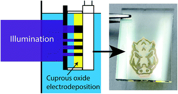
External fields can be used to regulate the morphological and chemical properties of electrochemically synthesized materials. One example is phototropism, where the coaction of light absorption and carrier generation can induce controllable variations in the material as it grows under illumination. Here we describe the photoelectrodeposition of photocathodic cuprous oxide (Cu2O). Illuminating the growing film with photon energies in excess of the band gap of Cu2O results in nanoscale morphological changes in the structure of thin films and intrinsically dopes the material during growth. The result is a ‘black’ Cu2O film that is chemically distinct but crystallographically identical to an ordinary film grown in the dark. The flat band potential of the film is controlled by the growth illumination intensity and the photodoping is reversible under thermal oxidation. We explore the nature of the intrinsic dopant, the emergence of nanocrystalline Cu metal inclusions in the Cu2O matrix, and the potential of for this effect to be used in the fabrication of new semiconductor heterostructures. This chemical distinction between the native and black Cu2O can be exploited to pattern films with a photomask as an example of direct photolithography.


 Please wait while we load your content...