
 Open Access Article
 This Open Access Article is licensed under a
 Creative Commons Attribution 3.0 Unported Licence
Updating the road map to metal-halide perovskites for photovoltaics
Peter D.
Matthews
 a,
David J.
Lewis
*b and
Paul
O'Brien
*ab
a,
David J.
Lewis
*b and
Paul
O'Brien
*ab
aSchool of Chemistry, University of Manchester, Oxford Road, Manchester, M13 9PL, UK. E-mail: paul.o'brien@manchester.ac.uk
bSchool of Materials, University of Manchester, Oxford Road, Manchester, M13 9PL, UK. E-mail: david.lewis-4@manchester.ac.uk
First published on 24th July 2017
Abstract
Metal-halide perovskites have revolutionised photovoltaics in a short space of time due to their large power-conversion efficiencies and flexibility in device processing. However, questions loom over the deployment of these materials in photovoltaic modules including those of long-term stability and reproducibility in performance. In this review we provide an update to this rapidly developing field.
 Peter D. Matthews | Peter D. Matthews studied for his M.Sc. at the University of Cambridge (2008–2012) and completed his Ph.D. (2012–2016) there with Prof. Dominic S. Wright and Prof. Ali Alavi, working on polyoxotitanate cages and heteroatom doped graphites. He has moved to the University of Manchester to take up an EPSRC Doctoral Prize with Paul O'Brien where his work focuses on metal chalcogenides for photovoltaic purposes. |
 David J. Lewis | David J. Lewis is a Lecturer in Functional Ceramic and Inorganic Materials in the School of Materials at the University of Manchester, U.K. He received M.Sc. and Ph.D. degrees in Chemistry at the University of Birmingham, U.K. in 2002 and 2006 respectively. He research interests lie in inorganic nanomaterials and thin films for a range of uses including alternative energy, catalysis and biological applications. He is a member of both the Royal Society of Chemistry (MRSC) and the American Chemical Society. |
 Paul O'Brien | Paul O'Brien CBE FRS FREng is Chair of Inorganic Materials Chemistry in the Schools of Chemistry and Materials at the University of Manchester; he was Research Dean 2000–03, Head of the School of Chemistry 2002–09 and Head of the School of Materials 2011–15. He has held academic positions at Chelsea, Queen Mary and Imperial Colleges in the University of London. He was awarded the Kroll, Sir Colin Humphreys and Platinum Medals of the IoM3 and the 1st Peter Day Award and the Longstaff prize from the RSC. His research centres on developing new chemical processes especially of metal chalcogenides. |
Introduction
The growing worldwide demand for energy security has resulted in an increased focus on finding ways of transforming sunlight into electricity in a sustainable and economically viable way. A number of different photovoltaic (PV) technologies have emerged beyond silicon cells, including dye sensitized solar cells (DSSCs),1,2 organic photovoltaics3 and various transition metal chalcogenide based devices,4 but in recent years a class of materials based on hybrid inorganic–organic materials have become the focus of intense research: metal halide perovskites (MHPs), which have the general stoichiometric formula of ABX3, where A is a monovalent cation, B is divalent metal cation and X is a halide anion.Initial research into MHPs focused on methyl ammonium lead iodide systems, i.e. CH3NH3PbI3, or MAPI for short. However, concerns about the environmental impact and general toxicity of lead have led some research groups to replace it with more benign tin.
Perovskite photovoltaics have enjoyed a rapid rise in development, with the maximum power conversion efficiency (PCE) increasing sharply from 3.8% in 2009 (ref. 5) to a certified 22.1% in 2016.6 In comparison, it took nearly 30 years for silicon PV devices to mature to such high efficiencies. This has inspired a new photovoltaic ‘gold rush’ and according to Thomson ISI's Web of Science there have been more than 1500 papers published on ‘photovoltaic perovskites’ with nearly 800 of those coming in 2016 alone.7
There are number of high quality reviews covering the broad aspects and the history of MHPs,8–20 as well as more detailed reviews on their stability,21–25 underlying physical properties,26,27 improvements in the hole-transport material they are paired with28 and post-synthetic transformations.29 There are also some reviews on synthetic routes to perovskites.30–32 In this short review we shall provide readers with an update on the state of the art in this rapidly evolving field.
Key structures
The chemical and electronic structure of ABX3 perovskite is shown in Fig. 1. The divalent metal cation, B2+, occupies an octahedral coordination site surround by six X− halide ligands, whilst the monovalent cation, A+, sits in a large cuboctahedral site in the middle of this. The idealised structure is a primitive cubic cell of A cations with face-centred X anions and the B-cation occupying the centre of the cube. However, changing the size of the monovalent cation, A, can result in a distortion to orthorhombic, rhombohedral or tetragonal symmetries.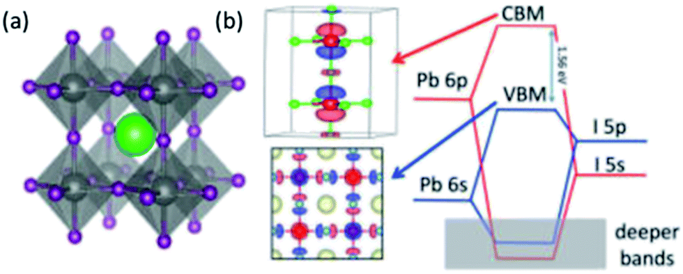 | ||
| Fig. 1 (a) The structure of ABXs perovskites. Green = A (i.e. MA, FA or Cs), grey = B (i.e. Pb or Sn) and purple = X (i.e. Cl, Br or I). (b) The band structure of ABX3 perovskites. Note that the valence and conduction bands are predominantly made up of the Pb-6p and the I-5p orbitals. The monovalent cation does not contribute. Reprinted with permission from ref. 8, ©2017 American Chemical Society. | ||
The band structure for APbI3 is shown in Fig. 1b. This indicates that the valence and conduction bands are predominantly made up of the Pb-6p and I-5p orbitals.8 The monovalent cation is mostly responsible for structural cohesion, but does have a minor direct contribution to the band gap, as well as a major secondary contribution. In the case of methylammonium (MA), there is a small contribution ∼0.5 eV below the valence band maximum (VBM).33 This suggests that there is an interaction between the MA and PbI6 octahedra, which is generally described as a hydrogen bonding interaction.34 The secondary contribution is due to the way in which the size of the monovalent cation can cause the PbI6 octahedra to distort/tilt. In turn, this tilting changes the band structure.18,29,35,36 Indeed, Motta et al. have demonstrated that the orientation of MA can exert strain on the octahedra, changing the band gap by ∼0.1–0.2 eV, depending on orientation.33 Recently, Selig and co-workers have shown that the dynamics of the MA orientation are dependent on the halides in the octahedra. They note that the cation dynamics increase with decreasing halide size, which they ascribe to the polarizability of the halide. They also note that using a mixed halide [i.e. MAPb(BrxI1−x)3] results in partial immobilisation of the cation.37
The stability of the structure, and by extension the size constraints of cation A is governed by the Goldschmidt tolerance factor (t).38 Adapting the tolerance factor to account for molecular ions occupying the A site gives the following equation:
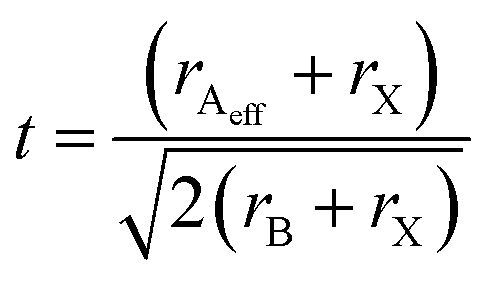 | (1) |
Methyl ammonium (MA) lead halide is by far the most studied system, but the MA is beginning to be replaced by the formamidinium ion (FA), as this results in a slight decrease in the band gap from 1.59 eV to 1.45–1.52 eV (ref. 44 and 45) through a change in the tilt of the PbI6 octahedra. Unfortunately, at room temperature FAPbI3 can easily convert from its photoactive cubic (or pseudocubic) structure to a photoinactive hexagonal structure. The cubic (or pseudocubic) structure can be stabilised by introducing small amounts of MA into the structure, leading to binary systems of (MA)x(FA)1−xPbI3.46–48
One of the great strengths of MHPs is that the electronic properties of the perovskite can be tuned by exchanging some of the iodide in the structure for bromide or chloride. Introducing Br expands the band gap, which can be useful for application in tandem solar cells. However, too much Br can lead to stability and phase segregation.44 The optimum composition for devices that demonstrate up to 21% efficiency is (FA)2/3(MA)1/3PbBr1/3I2/3.44,48,49 This composition is clearly a complex phase and presents significant synthetic challenges in terms of batch to batch reproducibility.
Lead free perovskites have not received the same level of attention, perhaps because the main candidate for the B site metal is divalent Sn, which is readily oxidised from photoactive Sn(II) to photoinactive Sn(IV). The 6s orbital of Pb is much more inert than the 5s of Sn, and so oxidation is not an issue which has been identified for Pb perovskites.50,51 However, there has been some recent interesting work into MASnI3 and CsSnI3, which has indicated that these systems are worthy of future investigation.52–54
Cell architectures
There are a number of different architectures for MHP devices, the four most common of which are summarised in Fig. 2. These can be grouped into two classes. In mesoporous cells (Fig. 2a and b), the MHP is decorated onto a mesoporous metal oxide (usually TiO2 although Al2O3 has also been used). These were the first cells to display the photovoltaic effect and are direct descendants of the Graetzel cell. Planar heterojunctions (Fig. 2c and d), which were later introduced by Snaith and co-workers have the perovskite deposited onto a flat substrate, usually compact TiO2.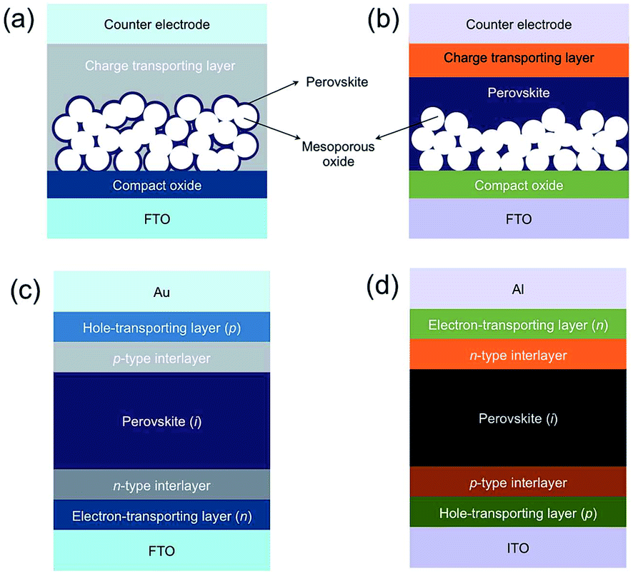 | ||
| Fig. 2 The four most common architectures for perovskite photovoltaic devices. Mesoporous heterojunction cells with (a) no perovskite overlayer and (b) with perovskite overlayer. Planar heterojunction solar cells with (c) conventional “n–i–p” and (d) inverted “p–i–n” configuration. Reprinted with permission from ref. 70, ©2015 Royal Society of Chemistry. | ||
The metal oxide layer acts as an electron transport layer (ETL), and in all cases the perovskite layer is sandwiched between this ETL and a hole transporting layer (HTL). A conventional cell has a “n–i–p” arrangement, i.e. the ETL (n-layer) on the bottom, followed by the perovskite (i-layer) and HTL (p-layer) on the top. In this classical architecture the ETL is typically TiO2, though Al2O3, SnO2, ZnO and La-doped BaSnO3, have also been used.55–59 The HTL is typically 2,2′,7,7′-tetrakis(N,N-di-p-methoxyphenylamine)-9,9′-spirobifluorene (spiro-OMeTAD), though this is very expensive and replacements are being sought. The top contact for devices is usually Au.
Conventional n–i–p cells demonstrate the highest efficiencies, however inverted p–i–n cells offer advantages in other ways. The processing temperature for the metal oxide layer in conventional cells can be quite high, and this can be avoided by using a metal oxide-free ETL in an inverted configuration. It should be noted that some metal oxides can be processed at lower temperatures.60 These systems use a HTL of poly(3,4-ethylenedioxythiophene):poly(styrenesulfonate) (PEDOT:PSS) (or equivalent) and a fullerene based ETL of phenyl-C61-butyric acid methyl ester (PCBM). Avoiding the need to anneal a metal oxide layer means that these systems may be suitable for roll-to-roll processing, making them more suitable for extensive manufacturing. The record PCE for inverted p–i–n systems is 18.2%,61 which lags somewhat behind the 22.1% of a conventional architecture but is nevertheless a promising result.
There have been some difficulties in comparing the maximum power conversion efficiency (PCE) figures for perovskites, as the current density–voltage (J–V) curves are heavily dependent on the scan profile used during the measurement. This manifests as an anomalous hysteresis in the J–V and results in PCEs that are overestimates of the true value.62–66 It appears that this hysteresis is caused by migration of I− ions within the lattice towards the HTL.67 A reduced hysteresis is observed in inverted cells that employ PCBM as a hole-blocking layer, though the origin of this is not yet clear.68,69
Synthetic routes
The range of synthetic routes to perovskite thin films for use in photovoltaics is almost as diverse as the range of compositions that have been studied. However, the main routes can be broken down into four broad categories. These are: one step, two-step, anti-solvent and vapour deposition routes (Fig. 3). Printing of films from nanocrystal inks,71,72 electrochemical deposition73 and gelation are also possible.74 All these routes take place without a special atmospheres, can take place at ambient pressure and temperature and do not require clean rooms or glovebox preparations.75,76 This is perhaps the greatest strength of perovskite photovoltaics; in general, the preparation routes are simple and can be performed by most modestly equipped materials laboratories.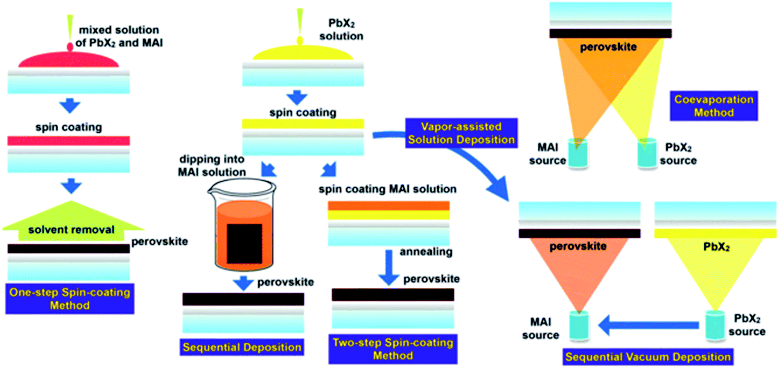 | ||
| Fig. 3 The synthetic routes to photoactive perovskite layers. Reproduced with permission from ref. 31, ©2015 Royal Society of Chemistry. | ||
One step
The one step route has been popularised by the group of Snaith,77 and is perhaps the simplest method for synthesising photoactive lead perovskite layers. In this method, a solution containing both the A cation (i.e. CsX, MAX or FAX, X = halide) and PbI2 is spin coated onto the TiO2 electrode and then annealed. This processing method is suitable for depositing on a mesoporous electrode as well as planar devices,78 but has proven particularly suitable for mesoporous layers as the nanoparticulate scaffold can be included in the precursor solution.79 One potential downside of the one step approach is that it results in poor surface coverage on flat surfaces due to dewetting effects, leading to unsatisfactory performance in planar heterojunction devices.80A typical one step process involves the dissolution of PbI2 and MACl in N,N-dimethylformamide (DMF), in a 1![[thin space (1/6-em)]](https://www.rsc.org/images/entities/char_2009.gif) :1 molar stoichiometric ratio and an approximately 0.1–0.2 M concentration. This is then spun into a film at relatively high rpm (3000–4000 rpm) before being annealed at ∼100 °C. Zhao et al. modified this approach to include tin(II) iodide (and MAI in place of MACl for the tin reactions) and produced a range of materials with the formula MA(PbxSn1−x)I3. They found that the inclusion of Sn allowed them to tune the band gap, with band gaps of 1.19 eV and 1.27 eV for x = 0.2 and 0.4 respectively. These devices, however, gave rise to PCEs of only ∼10%.81
:1 molar stoichiometric ratio and an approximately 0.1–0.2 M concentration. This is then spun into a film at relatively high rpm (3000–4000 rpm) before being annealed at ∼100 °C. Zhao et al. modified this approach to include tin(II) iodide (and MAI in place of MACl for the tin reactions) and produced a range of materials with the formula MA(PbxSn1−x)I3. They found that the inclusion of Sn allowed them to tune the band gap, with band gaps of 1.19 eV and 1.27 eV for x = 0.2 and 0.4 respectively. These devices, however, gave rise to PCEs of only ∼10%.81
The choice of solvent is limited by the poor solubility of lead halides in common organic solvents, and as a result polar, aprotic solvents such as DMF, dimethyl sulfoxide (DMSO), g-butyrolactone (GBL) and dimethylacetamide (DMA) are common.56,82,83 Noel discovered that both MAI and PbI2 could be dissolved in a combination of acetonitrile (MeCN) and methyl ammonia. The use of this composite solution resulted in an extremely smooth, pinhole-free material that exhibited long carrier lifetimes and a PCE of 18%.84
Classically, the ratio of precursors in solution has been 1:1 (for a simple binary system such as MAPbI3), which is the target stoichiometry of the film. However, there is some benefit to increasing either the organic cation or, conversely, using an excess of PbI2. An excess of MAI during the crystallisation process leads to the formation of very large crystalline grains, which should reduce hole–electron recombination at grain boundaries.85–87 Although if these domains grow too quickly there may be voids (often referred to as ‘pinholes’) left in between the crystal grains, resulting in poor surface coverage.88 Chen et al. have suggested that increasing the amount of PbI2 relative to MA gave improved solar cell performance owing to residual PbI2 passivating the grain surfaces.89 These two suggest that there are fine nuances to be considered when choosing the stoichiometry of the precursor solution.
It is important to note that subtle variations in the precursor solution can lead to major differences in device characteristics. These variations can manifest in structural and electronic defects,90 non-uniform film coverage91 and compromised crystallinity,92 which leads to poor performance. Rehman et al. have modified their standard procedure to include a 48 h ‘ageing’ step between preparing the solution and spin coating their electrode – though gave no reason for this.93 It was also found that perovskites with the general formula CsyFA(1−y)Pb(BrxI(1−x))3, have a window of stability for 0.10 < y < 0.30. Within this window, they found that the absorber layers in their devices were highly crystalline, possess high photo-stability against halide segregation and exhibit excellent charge-carrier lifetimes and mobilities.93
Tsai and co-workers investigated the ageing effect further by keeping a solution of MACl and PbI2 in DMF at 70 °C for 1–48 h. They found that the average grain size of the cast crystallites increased with ageing time, as did the overall crystallinity, MAbI3:MAPbCl3 ratio and device performance (Fig. 4).94 It is unclear why ageing the solution has this effect, but it indicates that when reporting research in the literature, care must be taken to report all of the conditions, as even simple one such as the age of the precursor solution have an important influence.
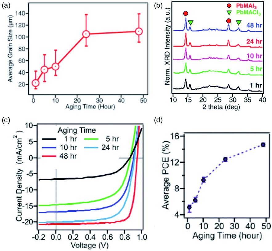 | ||
| Fig. 4 The influence of an aged precursor on the MAPbI3 layer. (a) Average grain size, (b) crystallinity as determined by pXRD, (c) J–V characteristic curves of devices and (d) power conversion efficiency (PCE) of devices. Adapted with permission from ref. 94, ©2017 WILEY-VCH Verlag GmbH & Co. KGaA. | ||
The inclusion of trace amounts of chloride ions has been previously shown to improve the morphology, increase the carrier diffusion length and enhance the overall optoelectronic properties in comparison to pure MAPbI3. Unfortunately, it is difficult to control the amount of chloride incorporated owing to the propensity to phase separate and form MAPbCl3, which has a band gap too wide for photovoltaic applications. Liao et al. have discovered a simple route to avoid these problems, by ‘hot-casting’ their solution, thereby enabling ultrafast crystallisation and encouraging the incorporation of Cl. To do this, they pre-heated their FTO/NiOx electrode (for an inverted cell) to 180 °C on a hot plate and transferred to a coater before quickly dropping 100 μL perovskite solution onto the hot substrate followed by spin-coating at 4000 rpm for 15 s. The film turned black in ∼4–5 s, indicating perovskite crystallization.95 This method, not unsurprisingly, results in small grain sizes.
In contrast to this, Sakai et al.97 have built on work by Nazeeruddin and co-workers,96 who suggested that the formation of larger crystals is directly related to a more relaxed lattice structure to force a more relaxed lattice through the inclusion of minor amounts of chloride. Inclusion of 2 mol% PbCl2 in the precursor solution resulted in monodisperse quadrilaterally-shaped crystallites of tens of micrometers in size. These crystals impinge on each other during growth to give pinhole free films, which could be incorporated into a device that presented a PCE of 19.1%.97
Both Cotella98 and Rao99 have adapted the one step method to a large scale processing procedure, which demonstrates its utility in a manufacturing set up.
A subset of the one step process is the ‘Lewis base’ approach, first suggested by Ahn in 2015,100 and since adopted by others.101,102 In this method, a 1:1:1 equimolar adduct of MAI, PbI2 and DMSO is prepared in DMF. The addition of DMSO as a Lewis base results in significantly smoother films than those prepared without it. If FA+ is to be used instead of MA+, then thiourea is a more appropriate Lewis base, increasing the crystallite size of FAPbI3 by 137%.103
The major challenge of using solvents such as DMF, DMSO and GBL are that they are relatively non-volatile and have both a high boiling point and low vapour pressure. This makes them hard to remove during the spin coating process, which may result in poor film coverage. Hendriks and co-workers have trialled the use of 2-methoxyethanol as an alternative solvent, as it has a much greater volatility than the traditional solvents. They found that this leads to a more rapid drying of perovskite precursor layers, leading to more compact layers of smaller crystals with fewer pinholes after annealing. They note that their method produces small crystal sizes, which results in the formation of multiple grain boundaries between crystallites. However, they found that their PCE increased from 14.1% for a DMF processed device to 15.3% for a 2-methoxyethanol one.104 This can be attributed to the increased surface coverage of their film, which indicates that there is a complex interplay between surface coverage and number of grain boundaries that influences the PCE.
Bai et al. have reported that even though they carry out their depositions in a controlled humidity environment, they still observe visible defects in the coverage of their films. In order to improve the surface of the their films, they have compared ‘air-drying’ with the ‘anti-solvent’ approach, the latter of which is discussed in more detail below.105 They found that adopting a relatively slow two step spinning process (1200 rpm for 25 s followed by 2000 rpm for 12 s) and then gently blowing an inert gas (i.e. ‘air-drying’) onto the film for 30 s accelerated the nucleation process.106 The quality of the film, however, was dependent on the atmospheric condition in the drybox, the distance between substrate and gas inlet, the gas flow rate and the degree to which the substrate was ‘gently rocked by hand’ which suggests a significant degree of subjectivity to the synthesis. They compared this ‘air-drying’ process to the anti-solvent method, and found little differences between the two, though both represented improvements over the standard procedure.
Ding and co-workers have developed a similar technique to that of Bai's ‘air-drying’ method, which they refer to as the gas-flow-induced gas pump method (GGPM). In this method a dynamic vacuum is applied to a freshly deposited film of MA0.9FA0.1PbI3 from above, whilst an inert gas is blown on the sample from the side. They found that the lower pressure systems (100 Pa) gave an extremely uniform film, which they attribute to rapid nucleation and growth owing to very fast solvent evaporation. Their champion cell gave a PCE of 20.24%.107
The one-step approach has also seen innovation in the precursors used. Lead halides have been switched for lead acetate, with MAI and MACl the sources of methyl ammonium and halide.104,108–111 Pb(OAc)2 derived devices have achieved good performance, with Zhao et al. reporting a champion PCE of 18.3%.109 It is interesting to note that Soufiani et al. observe the formation of large grain sizes using Pb(OAc)2.110 An observation that is possibly also related to the fact that they use Pb(OAc)2·3H2O, which seems a little idiosyncratic given their otherwise strict use of anhydrous conditions. However, this does tie in with reports that suggest small amounts of water are beneficial to crystal growth.112,113
Anti-solvent method
The use of an anti-solvent, i.e. the addition of a liquid that the desired product is not soluble in, is a well-known approach to growing crystals in synthetic chemistry. In general, an anti-solvent diffuses into the solvent, gently changing the solubility of the product so that it enters the crystal growth regime. This principle is utilised by many researchers to grow perovskite films, whereby a one-pot solution is deposited and an anti-solvent is dripped onto the substrate during the spin-coating procedure.114,115 This can lead to the formation of an intermediate phase containing the solvent, which is removed upon heating.114 Typical anti-solvents in these procedures are toluene116 or chlorobenzene.117–119 The quality of the obtained film is heavily dependent on the dispensing speed of the anti-solvent.105,106 Although the anti-solvent approach is technically a modification of the one step method, it so ubiquitous that it has become a well-established method, and sub-field of study, in its own right.The use of an anti-solvent has several advantages over the one-step method. Firstly, if a volatile anti-solvent is used, this can help to wash away non-volatile precursor solvents such as DMF or DMSO. Secondly, it aids supersaturation of the precursor solution, which during the conventional one-step method only occurs due to solvent evaporation. This can result in secondary nucleation, leading to poor quality films. The anti-solvent causes supersaturation of the precursor solution, suppressing secondary nucleation and results in high quality, uniform films.
There seems to be little consensus as to the optimum spin speed, volume of anti-solvent addition or rate of addition. Indeed, the volume of anti-solvent used in literature spans a range of over 3 orders of magnitude from 20 μL (ref. 120) to 100 mL.121 It is highly likely that these factors are also linked to the concentration of perovskite precursor, as well as the type of perovskite that is to be deposited.
One strategy that has been used to boost efficiency of MHP devices is to include electron-deficient aromatic compounds such as nitrogen containing polycyclic aromatic hydrocarbons (N-PAH) in the absorber layer, which helps to passivate electron trap states on the surface of the crystals.86 these compounds are not soluble in DMF, but are soluble in diethyl ether/chlorobenzene, which are typical anti-solvents. Recently Ngo et al. have reported a method for passivating their MHP layers by dissolving the N-PAH in their anti-solvent, which lead to a decrease in hole–electron recombination in their films.122 This approach has also been carried out by Kumar and co-workers, who used perylene-3,4,9,10-tetracarboxylic dianhydride as an additive with chloroform as the anti-solvent.123
Ye et al. have attempted to improve upon the method of anti-solvent addition by spraying the anti-solvent onto the precursor solution, instead of dripping it during spin coating. They used a compressed gas system to spray small droplets of anti-solvent during the spinning process, and reported that in doing so they improved the integrity of the film.124 In a standard anti-solvent procedure, the precursors solvent may evaporate too quickly causing cracking,125 or the anti-solvent may cause circular ripples if dripped from too great a height or in too large drops. They claim that spraying smaller droplets across the entire surface can reduce these effects. To do this they used a custom spray equipment consisting of a solution dispersion system with a 10 mL container, a compressor to provide spray droplet carrier air flow, a glass nozzle and air flow as a pump to manage delivery of the solution from the dispersion container into the spray nozzle.124 Whilst this method of delivery may result in an improved film, the very nature of the ad hoc delivery system is not good for inter-lab reproducibility.
Pool and co-workers used the standard procedure to synthesise FAPbI3 with toluene as the anti-solvent, using a hot plate in the annealing step for thermal annealing. This allowed them to study the formation of FAPbI3via in situ pXRD, and they discovered that the commonly used annealing conditions for FAPbI3 of 10 min at 170 °C can be reduced to 40 s at 170 °C without changing the photovoltaic performance, which is a nice result for efficiency of preparation.
Yu et al. have shown that an anti-solvent (hexane) that is immiscible with the precursor solution can lead to controlled morphologies of perovskite layers. They called this the ‘interface precipitation’ (IP) method, as initial nucleation occurs at the interface of the solvent and anti-solvent.120 In their system, the initial nuclei grow at the solvent interface and then drop onto the mesoporous TiO2 scaffold. This decreases the supersaturation and stops further growth. After this, the anti-solvent evaporates first, being more volatile than the precursor solvent, and the mechanism then appears to follow the standard one-step procedure (Fig. 5). This is an interesting take on the anti-solvent procedure, which of course usually requires miscible liquids. One potential benefit is that they demonstrate control over the obtained morphology. Varying the amount of hexane they added they could obtain materials that were fairly porous (small amounts of hexane – growth dominated by evaporation of DMF) to densely packed (large amounts of hexane – growth dominated by primary nucleation).
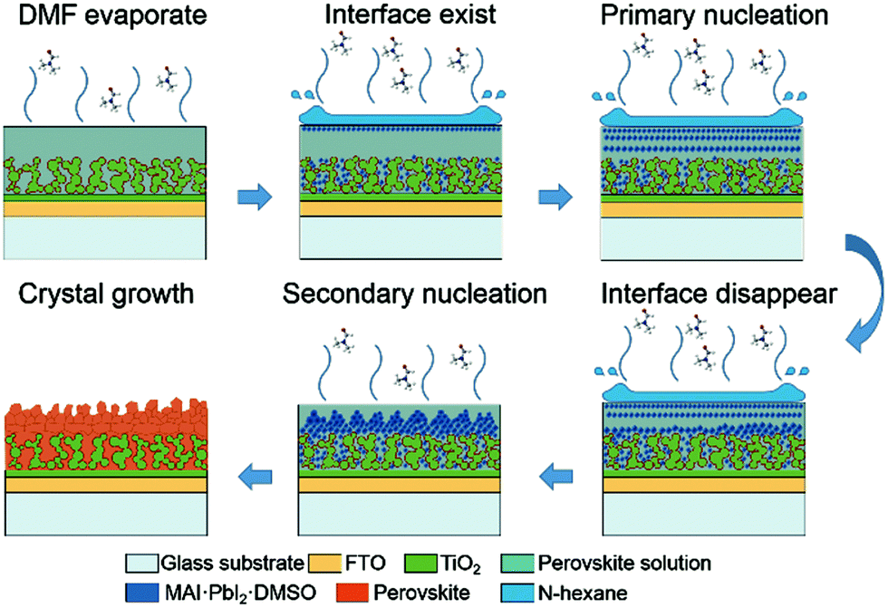 | ||
| Fig. 5 Schematic representation of nucleation and crystal growth during the interface precipitation (IP) method. Note that the first five steps take place during the spin-coating process and the last step takes place during the annealing process. Reprinted with permission from ref. 120, ©2017 Royal Society of Chemistry. | ||
One other anti-solvent that shows promise is ethyl acetate, which appears to act as a moisture absorber during spin-coating. When a hydrophobic anti-solvent such as toluene is dropped onto the MAI-PbI2 layer, this can result in the trapping of atmospheric moisture within the perovskite layer – leading to future degradation. However, ethyl acetate is significantly more hydroscopic and so the authors attribute the improved performance to it absorbing moisture from the surface of the perovskite.126
Two step
The two step method involves the deposition of a layer of PbI2 followed by exposure to the monovalent cation, either in solution127 or in vapour form.128,129 The key feature of this procedure is that the monovalent cation intercalates between the PbI6 octahedra to transform the PbI2 to APbI3 (A = Cs, MA, FA).52,130 As mentioned previously, MA+ is a smaller cation than FA+, and so it intercalates more easily than FA+, which requires a higher temperature.131In a typical procedure, a layer of PbI2 is deposited, either from a solution in DMF (or other appropriate solvent) or sputtered onto the substrate. Next a solution of the chosen monovalent cation halide (i.e. MAI), preferably dissolved in a solvent that PbI2 is not soluble in is then spin coated on top. Alternatively the PbI2 layer may be dipped into a solution containing MAI/FAI.132 The use of solvents such as iso-propanol in this second step prevent any loss of lead iodide.133,134 The bilayer films are then annealed to allow diffusion of the cation into the PbI6 lattice.
There are some disadvantages of the two step method, namely that the PbI2 layer can form a dense layered film, which might lead to incomplete conversion – residual PbI2 results in poor photovoltaic performance.135 Increasing the length of time of the reaction can address this issue, but can also lead to dissolution of the perovskite. Thermal annealing aids conversion to the perovskite form.90
Petrov et al. have combined the Lewis base approach with the two step method to generate MAPbI3 and FAPbI3 nanowires by dipping PbI2 films into solution containing MAI or FAI and DMF.136 They have posit that the size and shape of the nanowires is dictated by a topotactical transformation from the MAI/FAI–PbI2–DMF adduct obtained from the dipping procedure. This control over the morphology opens up the possibility of further compositional modification via ion-exchange to form MAPbBr3, MAPbCl3, and FAPbBr3 nanowires.136
A recent kinetic study of the two step method by Ko et al. investigated the effect of the processing conditions on the morphology of the perovskite layer. They found that the transformation from the two separate layers of PbI2 and MAI occurred in two distinct steps. First, MAPbI3 nucleated on the lead iodide surface and continued to grow until the surface was covered. This step is key to determining the surface morphology of the final product. The second step consisted of the remaining conversion of the PbI2 underneath the top layer. Overall, they found that the average grain size (R) is related to the rate of the initial growth (r) by R ∝ r−1/3, which is an important relationship that should help guide future work.137
Hsieh et al. have investigated the effect of the length of time spent dipping the PbI2 layer into a solution of MAI has on the final layer.138 In agreement with Ko, they report that the formation of MAPbI3 crystals from PbI2 and MAI involves an initial period of interfacial reaction. This is then followed by a period of dissolution–recrystallization (Fig. 6). The best material for photovoltaic devices is found at the transition between these two periods because the perovskite has been fully formed and the perovskite grains in the mesoporous TiO2 have yet to be dissolved. Longer dipping times lead to the formation of large crystals of MAP, but these demonstrate poor electron transport and are therefore suboptimal for devices.138
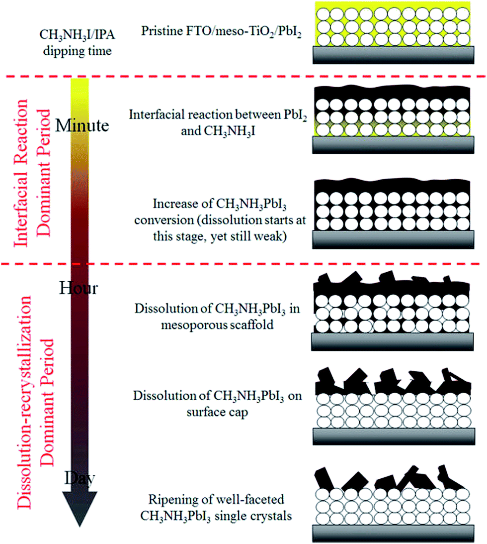 | ||
| Fig. 6 Crystal growth during the dipping of a PbI2 layer into a solution of MAI in iso-propanol. Reprinted with permission from ref. 138, ©2017 American Chemical Society. | ||
Zhang et al. proposed a two step route to high quality films that avoid both long reaction times and an annealing step by exposing the PbI2 film to pyridine vapour.139 This vapour induces the formation of nanostructured PbI2·(pyridine)2 films, which easily transformed to MAPbI3 by dipping into a solution of MAI in iso-propanol. They reported that their champion device had a PCE of 17.1%, which is very good for a room-temperature solution processed device.
Chiang and co-workers have discovered that the inclusion of small amounts of H2O in the MAI/iso-propanol solution gives rise to a H2O-rich perovskite phase after first treatment. If this material is annealed then the result is medium-sized grains of MAPbI3. However, if the film is treated with DMF vapour prior to being annealed then very large grains of MAPbI3 are formed (Fig. 6). This synergistic effect of a H2O/DMF treatment gave p–i–n inverted cells a PCE of 16.7%.140
Vapour deposition
In this context, vapour deposition is taken to cover a broad range of techniques that have each acquired their own acronym and following. Here we will discuss vacuum deposition techniques, as well as atmospheric vapour deposition processes.Vacuum deposition for perovskites is not as common as solution processing routes, but it is a technique that is widely used for the deposition of other semi-conductors.141,142 Thermal vapour evaporation (TVE) involves subliming a compound under a vacuum and with heating, and then allowing the desired phase to condense onto a target surface. There are two ways of generating MAPbI3 with this technique: co-evaporation involving the simultaneous evaporation of MAI and PbI2 (ref. 91) and a two step evaporation with the precursors evaporated and deposited sequentially.143 TVE allows the simultaneous deposition of perovskite films of identical composition on multiple devices, which Patel et al. utilised to investigate how different device architectures affect the J–V characteristics of a device.144 They found that the interface between the perovskite and the electron transport layer (ETL) is key, whilst the choice of ETL is critical in preventing hysteresis in the J–V curves. Their devices which had a layer of [6,6]-phenyl-C61-butyric acid methyl ester (PCBM) on top of TiO2 as the ETL, showed minimal hysteresis.
Chen et al. have extended the co-deposition TVE process to include CsPbI3 and CsPbI2Br, using films of PbI2 and CsI or CsBr as the precursors. In this case their perovskite films required an annealing step of 325 °C to form a crystalline material.145 Their device PCE was 11.5%, which was slightly greater than Frolova and co-workers, who followed a similar procedure.146
Tavakoli has adapted the co-evaporation method into a layer-by-layer approach, whereby alternating layers of PbI2 and MAI are vacuum deposited.147 They report that this method led to an improvement in carrier lifetime and a device with a PCE of 16.6%.
Non-vacuum vapour deposition processes include aerosol assisted chemical vapour deposition (AACVD) and spray deposition. In these techniques the relevant precursors are dissolved in a solvent and then atomised by a spray or ultrasonication before being deposited onto a hot substrate.148–152 The advantage of AACVD techniques are that they proceed at ambient pressure and are potentially scalable.
Stability
The most significant barrier to widespread implantation of MHP devices is the instability of the perovskite absorber layer in standard operating conditions. The major causes of decomposition are moisture, temperature, oxygen and UV light.22,153–155Water is a complex issue for OHPs. It is clear that water damages the perovskite layer, however it has also been reported that films grown in ∼30% humidity have improved morphology (larger grain sizes, fewer pinholes) and optoelectronic properties than films annealed in dry, O2-free gloveboxes.75,156,157 Water-catalysed degradation of MAPbI3 it thought to proceed through two main models: (i) the loss of nitrogen in the form of ammonia (eqn (2))158,159 and (ii) the decomposition of MAPbI3 into MAI and PbI2 (eqn (3)).160
 | (2) |
 | (3) |
In a recent study Ke et al. have shown through a near ambient pressure X-ray photoelectron spectroscopy (NAPXPS) study that water vapour induces a complete transformation of MAPbI3 to a mixture of Pb, PbI2 and hydrocarbon species, with the complete loss of N from the surface. This is consistent with the first degradation pathway, demonstrated in eqn (2), which clarifies the debate between the two models.24
Whilst there is an apparent benefit to growing films in a mildly humid environment,75,156 it is also clear that water is bad for the long term stability and functioning of a device. There have been a variety of interesting approaches to prevent water degradation, such as applying hydrophobic coatings or using hydrophobic hole transport layers (HTLs).161–167 Salado et al. have measured the water contact angle (WCA) for poly(3-hexylthiophene-2,5-diyl) (P3HT) and 2,2′,7,7′-tetrakis(N,N-di-p-methoxyphenylamine)-9,9′-spirobifluorene (spiro-OMeTAD), two of the more common HTLs. They report that MAPBI3/P3HT system has a WCA of > 100°, and is therefore hydrophobic, whereas MAPBI3/spiro-OMeTAD has one of <80° and is hydrophilic.168 This would indicate that simply choosing an appropriate HTL can improve the moisture stability of a MHP device. Likewise, when comparing stability reports in the literature it is important to consider the entire composition of the device. Salado also reported that the mesoporous triple cation system of Saliba,169i.e. Cs/MA/FA, in their case with the formula (Cs0.05(MAPbBr3)0.15(FAPbI3)0.85), has a lower rate of degradation than the classic MAPbI3. The added stability derives from the lower volatility of Cs+ compared to MA.
Other approaches to improving water stability are to exchange the iodide anions for thiocyanate pseudohalides. These are considerably more tolerant to water stability, and although initially had a relatively poor efficiency, they have recently improved to 16% PCE by introducing a mixed cation (Fa0.9Cs0.1) system.170,171
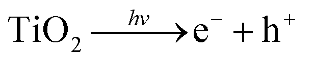
Water, oxygen and UV degradation pathways are most certainly interlinked with each other.172 Under UV irradiation the TiO2 electron transport layer (ETL) can promote an electron into its conduction band (eqn (4)), which facilitates the formation of hydroxyl radicals from ambient oxygen and water (eqn (5) and (6)). These hydroxyl radicals, as well as the holes in the TiO2 valence band can oxidise I− in the perovskite lattice (eqn (7) and (8)), leading to loss of I2 (eqn (9)). Iodine vapour has an additional negative impact by causing a chain reaction of perovskite degradation.173 Complete replacement of iodide for bromide (i.e. MAPbBr3) has a major stability benefit,25,172 though it should be remembered that it has a much wider band gap and as such is less suited for photovoltaic applications.174
 | (4) |
| CH3NH3+ + H2O ⇌ CH3NH2 + H3O+ | (5) |
| 3e− + O2 + 3H+ → H2O + HO˙ | (6) |
| HO˙ + I− → I˙ + HO− | (7) |
| h+ + I− → I˙ | (8) |
| 2I˙ → I2 | (9) |
Doping a MAPbI3 layer with CsX (X = Cl, Br) can have a remarkable benefit to the UV stability, as well as the aforementioned increase in moisture tolerance. CsCl or CsBr can work as a blocking layer between the TiO2 and MAPbI3 layers (Fig. 7), preventing the titania inducing radical formation.175,176
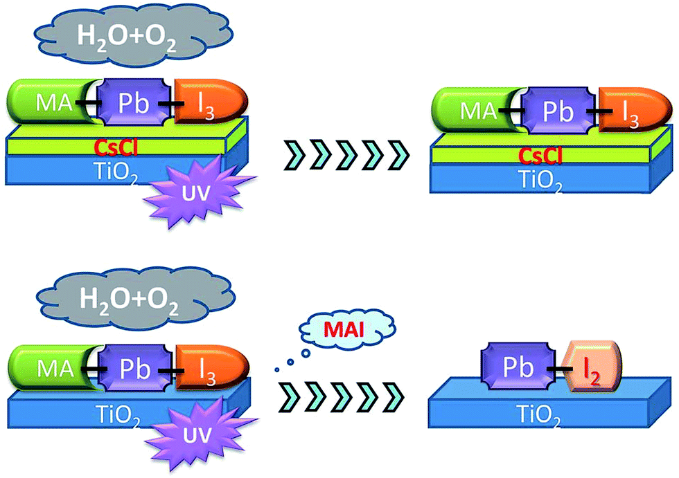 | ||
| Fig. 7 Schematic showing how CsCl can prevent the TiO2 ETL inducing radical formation under UV irradiation. Reprinted with permission from ref. 175, ©2016 Royal Society of Chemistry. | ||
Other options to improve stability under intense UV soaking are to exchange the mesoporous titania for a mesoporous Al2O3 scaffold155 or mesoporous SnO2.177 In comparison to TiO2, the latter has a wider band gap (3.6 V 3.2 eV),178,179 better electron injection from MHPs56 and higher electron mobility.180 However, SnO2 mounted on FTO leads to F− migration into the tin oxide layer, reducing electron selectivity. On the other hand, SnO2 based devices have demonstrated low open circuit voltages (VOC) and their max PCE leaves a lot of room for improvement.177
A certain amount of heat will accumulate in MHP devices during the course of standard operation, which can prove challenging to reduce. It is expected that the internal temperature of a device might reach 85 °C.181 This is most unfortunate, as MAPbI3 has been shown to decompose to PbI2 with the loss of gaseous MeNH2 and HI when heated to temperatures >85 °C.182,183 There have been various attempts to prevent thermal degradation by exchanging the Au top contact for carbon nanotubes184 or other carbon materials.185,186
It is likely that thermal (in)stability is also related to the water and oxygen derived decomposition processes described above. Niu et al. have shown that Cs doping can aid in thermal stability – though they note that their Cs-free MAPbI3 films are stable when heated under an inert N2 atmosphere.187 This would seem to indicate that the Cs prevented degradation in a manner as seen previously.188
A similar observation was noted by Zhao et al., who described that their MAPbI3 layer was intrinsically stable when heated to 120 °C in an inert atmosphere. However, they also observed substantial degradation when spiro-MeOTAD was used as the HTL.189 This is also possibly related to the hydrophilic nature of spiro-MeOTAD explained earlier.
Device optimisation
The architecture of perovskite solar cells is fairly complex (Fig. 2), and there are a lot of variables that can be improved upon to optimise device performance. In terms of the perovskite layer, we have discussed in length some of the techniques that have been used to improve PCE, but it is important to draw out some of the themes present, as well as the challenges that remain.In considering the composition of the perovskite, it is apparent that the acidity of the proton on the ammonium cation (both MA+ and FA+) is partly responsible for degradation processes. These can be mitigated by the use of inorganic cations such as Cs+, but this comes at a reduction in the dielectric constant, wider band gap and the photoactive form of CsPbI3 is not stable at room temperature.190–192 It would appear that the optimum combination of stability and electronic structure is a material that has the general formula: CsxMAyFA1−x−yPb(IzBr1−z)3.
Secondly, the morphology of the MHP layer. There are two factors at play here: (i) film coverage (i.e. pinhole free material) and (ii) grain boundaries. The best devices are pinhole free, as this represents the best surface coverage. However, this may be achieved by a rapid nucleation, with small, densely packed crystallites, or a slow crystal growth where the crystals impinge upon each other but continue to grow. Fewer grain boundaries means fewer trap/recombination sites, and is generally seen with larger crystal domains. However, large crystals sometimes pack poorly, resulting in pinholes. The upshot of this is that there is that coverage and number of grain boundaries is often traded off against each other.
The perovskite absorber layer is of course highly important, but equally so are the electron and hole transport layers (ETL and HTL). These layers act to prevent charge recombination and aid current flow.
Numerous HTL materials have been explored, including organic small molecules and conjugated polymers. The most common is 2,2′,7,7′-tetrakis[N,N-di-p-methoxyphenylamine]-9,9′-spirobifluorene (spiro-OMeTAD) for conventional n–i–p devices, with polytriarylamine, 2′,7′-bis(bis(4-methoxyphenyl)amino)spiro-[cyclopenta[2,1-b:3,4-b′]dithiophene-4,9′-flurene] (FDT) being used in some of the highest efficiency devices. For inverted p–i–n devices poly(3,4-ethylenedioxythiophene) polystyrene sulfonate (PEDOT:PSS) is the most used HTL. The HTL is one of the most expensive layers in a device, as substrates such as spiro-OMeTAD are extremely expensive.49,169,193,194
Huang et al. have sought to improve upon PEDOT:PSS by including DMSO into the PEDOT:PSS layer, which they find increases the charge extraction and photocurrent.195
Xi and co-workers have reported that the inclusion of a redox active dopant, in their case either lithium bis(trifluoromethane)sulfonimide or a cobalt based dopant into spiro-OMeTAD, improved hole mobility.196 However, other authors note that this severely impacts the lifetime of the spiro-OMeTAD.163
Spiro-OMeTAD features in most of the highly efficient MHP devices, but it is a relatively expensive material, owing to its challenging synthesis. It has often been described as the best HTL,197 but as we have discussed above, it promotes degradation of the perovskite layer and replacements should be sought. Nazeeruddin et al. have recently developed a new class of HTL based on a benzo[1,2-b:3,4-b′:5,6-b′′]tri-thiophene core with electron-donor groups attached, which they use in devices with PCE >18%.198,199
Ahmadi et al. have trialled a different HTL that also features a thiophene core, thieno[3,4-b]-thiophene-alt-benzodithiophene (PTB7), which they compared to poly(3-hexylthiophene) (P3HT). PTB7, unlike P3HT, has a photoinduced dipole, and the authors demonstrate that this can decrease charge recombination in the perovskite layer. Additionally, the photoinduced dipole decreases charge accumulation at the electrode interface.200
Organic HTLs may be simple to process, but it is highly likely that they will degrade over time under the operating conditions of a photovoltaic cell. To this end, inorganic HTLs offer superior long-term stability, and a number of different species have been assessed for conventional p–i–n cells, including CuGaO2, CuSCN, Co-doped NiOx, SnO2, and ZnO.201–206 Amongst these, CuSCN has achieved PCEs >11%,202,207 NiOx has reached a PCE of 16.1% (ref. 206) and recently Zhang et al. have improved this to 18.5% with CuGaO2.201 These inorganic HTLs are not without problems, as CuSCN can induce degradation of MHPs,208 and the NiOx usually requires a high temperature annealing step, limiting its use to inverted devices. Recently, Cao et al. have reported the use of a NiOx nanoparticulate ink, which does not require an annealing step and therefore allows the deposition of the NiOx HTL at room temperature, allowing its use in conventional cells.209 It is worth noting though that the stabilising ligands on the surface of the nanoparticles can act as charge carrier insulators, which is detrimental to the performance of thin films derived from nanoparticulate inks.210
The electron transport layer (ETL) is predominantly based upon TiO2, with the main difference being whether the metal oxide is mesoporous or planar (Fig. 2). One method to encourage a good contact between a metal oxide ETL and the perovskite layer is to place a self-assembled monolayer of bifunctionalised organic molecules that can bond to both the metal oxide and the MHP.211,212 This approach is typified by Zuo et al., who used 4-pyridinecarboxylic acid (PA) as a SAM between an SnO2 electrode and MAPbI3, resulting in a PCE improvement of 10% for their devices.213
For inverted architectures, there are few ETL candidates that are not metal oxides, with the majority that are being based around fullerene (C60) or its derivatives such as [6,6]-phenyl-C61-butyric acid methyl ester (PCBM). The benefit of an organic ETL is that it can be processed at a much lower temperature than the metal oxide, and is far more useful in the context of flexible devices. Small organic molecules have a further advantage over PCBM owing to their simple synthesis. If they have sulfur in their structure then this might improve the interfacial interaction between the ETL and perovskite through an S–Pb bond.214 Gu et al. have used this reasoning to develop 10,14-bis(5-(2-ethylhexyl)thiophen-2-yl)-dipyrido[3,2-a:20,30-c][1,2,5]thiadiazolo[3,4-i]phenazine (TDTP) as the ETL with a PCE of 18.2%.61
Bai and co-workers have revisited fullerene polymers as the ETL in an inverted planar device, but this time they crosslinked the fullerenes with a siloxane that also featured a hydrophobic tail (Fig. 8). Not only did their device perform admirably, with a PCE of 19.5%, but the dual function ETL enhanced the perovskite stability to moisture. The hydrophobic tail of the ETL ensured that their devices retained nearly 90% efficiency after 30 days exposure to an ambient environment, which represents remarkable progress.215 Combining an ETL (for inverse) of HTL (for conventional) with a hydrophobic coating represents good progress in terms of device processing simplicity and efficient material usage. This seems an appropriate goal for ‘green’ energy devices such as solar cells.
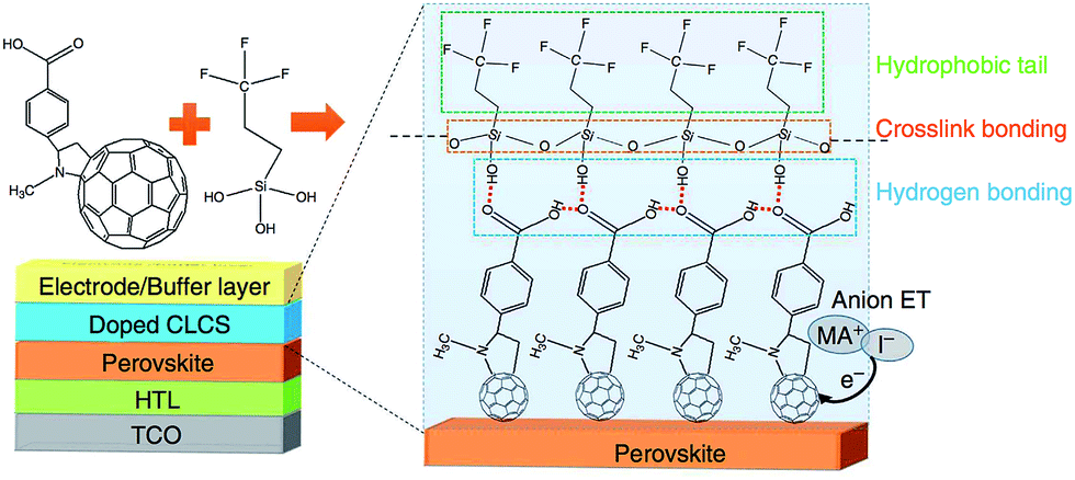 | ||
| Fig. 8 A fullerene based ETL with a hydrophobic backbone that aids stability towards moisture-based degradation in an inverted p–i–n device. Reprinted with permission from ref. 215, ©2016 Nature Publishing Group. | ||
One area that has been much studied is how the presence of additional PbI2 affects the overall performance of a perovskite solar cell. If there is a poor conversion of PbI2 to the desired perovskite phase then this can have a detrimental effect, as the remaining PbI2 is photoinactive.216 However, a thin veneer of lead iodide on the surface of the perovskite grains passivates their surface and results in improved carrier transport,89 as defects in the surface act as trap states.217 Shih et al. have recently applied light-modulated scanning tunnelling microscopy (LM-STM) to study the interface between MAPbI3 crystals and a PbI2 passivation layer. From this work, they conclude that a passivation layer of <20 nm is desirable for the optimum reduction in charge carrier recombination.218 This was echoed by a study from Du and co-workers.219
The crystal orientation in the MHP layer is not something widely considered, but Bae et al. have reported that it can have a dramatic impact on the performance of devices. For an inverted planar heterojunction device the (112) and (200) planes should be parallel to the substrate for optimum performance, whereas for a normal planar heterojunction then the (002) and (110) planes should be parallel to the substrate.220
Finally, there have been numerous attempts to modulate the perovskite film morphology by including organic molecules,221 polymers,222 or silica.223 Zhang et al. have taken this one step further by seeking to include a polyoxometallate (POM) into their MAPbI3 layer. This resulted in Ostwald ripening during the crystal growth period, i.e. larger grains merged with the smaller grains. Their device showed a respectable PCE of 11.35%, which is notable as they did not include a HTL as the POM should perform that function.224
To improve the overall performance and stability of perovskites, a number of researchers have looked away from lead and tin to study other options such as bismuth iodide225–227 and chalcogenide perovskites.228 Zhao et al. have performed a computational screen of Pb-free halide perovskites by considering exchanging one divalent Pb2+ for one monovalent MA+ and one trivalent MB3+, giving the quaternary compound A2MAMBX6. The two most promising compounds they found were Cs2InSbCl6 and Cs2InBiCl6, which both have a direct band gap of 1.0 eV and show theoretical maximum solar cell efficiencies comparable to that of MAPbI3.229 It will be very interesting to see if the compounds can be synthesised and tested to compare the experimental data to this very promising theoretical result.
In an experiment that is similar to what Zhao suggested, Klug et al. have experimentally replaced small amounts of Pb in MAPbI3 with nine divalent metal ions (Co, Cu, Fe, Mg, Mn, Ni, Sn, Sr, and Zn). They found that the perovskite structure is reasonably tolerant to partial substitution, with the best PCE coming when <6% of the Pb2+ is replaced with Co2+.230 This offers another opportunity to fine tune the electronic properties of the perovskite, in addition to substituting the halide and the monovalent cation.
Future outlook
This short perspective has sought to summarise some of the most recent key results in what is perhaps the fastest moving materials science area aside from graphene. Major areas of recent interest include significant advances in the synthetic protocols that give rise to devices of ever increasing quality. What is clear from a review of the literature is that the rapidly moving nature of the field has been its major downfall in some respects; the PCEs reported have risen so rapidly to levels which may allow commercialisation, but the materials science and chemistry, often crucial in defining the underlying physical principles which guides subsequent research, has at times lagged behind. As a result phenomena such as instability in humid atmospheres and the anomalous hysteresis in the J–V curves, discovered post-fact, are still not fully understood though consensus seems to be emerging. It is also clear that there is not yet an optimum device composition, as variations in perovskite/ETL/HTL all have remarkable effects on device efficiency and life time.Future directions in the field will potentially focus on producing stable materials that may resist decomposition in humid atmospheres, understanding and eliminating the anomalous hysteresis effects that have plagued device quantification and reporting of PCEs as well as focusing on elimination of toxic lead in the formulations. All of this whilst maintaining high PCEs, ensures that this field has many challenges ahead.
Acknowledgements
The authors acknowledge funding from the EPSRC with grants EP/K010298/1 and EP/K039547/1 (POB) and a Doctoral Prize for PDM (grant EP/M507969/1). POB also thanks The Royal Society DFID Africa Capacity Building Schemes for their financial support. This review is dedicated to the memory of Russell Binions (QMUL).Notes and references
- B. O'Regan and M. Grätzel, Nature, 1991, 353, 737–740 CrossRef.
- K. Meng, G. Chen and K. R. Thampi, J. Mater. Chem. A, 2015, 3, 23074–23089 CAS.
- W. R. Mateker and M. D. McGehee, Adv. Mater., 2017, 29, 1603940 CrossRef PubMed.
- P. D. Matthews, P. D. McNaughter, D. J. Lewis and P. O'Brien, Chem. Sci., 2017, 8, 4177–4187 RSC.
- A. Kojima, K. Teshima, Y. Shirai and T. Miyasaka, J. Am. Chem. Soc., 2009, 131, 6050–6051 CrossRef CAS PubMed.
- M. A. Green, K. Emery, Y. Hishikawa, W. Warta and E. D. Dunlop, Prog. Photovoltaics, 2016, 24, 905–913 Search PubMed.
- Web Sci. search with search terms ‘photovoltaic perovskite’, accessed 24-04-2017.
- M. Grätzel, Acc. Chem. Res., 2017, 50, 487–491 CrossRef.
- M. Grätzel, Nat. Mater., 2014, 13, 838–842 CrossRef PubMed.
- J.-P. Correa-Baena, A. Abate, M. Saliba, W. Tress, T. J. Jacobsson, M. Gratzel and A. Hagfeldt, Energy Environ. Sci., 2017, 10, 710–727 CAS.
- H. S. Jung and N. G. Park, Small, 2015, 11, 10–25 CrossRef CAS PubMed.
- N. G. Park, Mater. Today, 2015, 18, 65–72 CrossRef CAS.
- M. He, D. Zheng, M. Wang, C. Lin and Z. Lin, J. Mater. Chem. A, 2014, 2, 5994–6003 CAS.
- M. A. Green, A. Ho-Baillie and H. J. Snaith, Nat. Photonics, 2014, 8, 506–514 CrossRef CAS.
- S. D. Stranks and H. J. Snaith, Nat. Nanotechnol., 2015, 10, 391–402 CrossRef CAS PubMed.
- S. D. Stranks, P. K. Nayak, W. Zhang, T. Stergiopoulos and H. J. Snaith, Angew. Chem., Int. Ed., 2015, 54, 3240–3248 CrossRef CAS PubMed.
- H. J. Snaith, J. Phys. Chem. Lett., 2013, 4, 3623–3630 CrossRef CAS.
- A. R. Bin, M. Yusoff and M. K. Nazeeruddin, J. Phys. Chem. Lett., 2016, 7, 851–866 CrossRef PubMed.
- W. Li, Z. Wang, F. Deschler, S. Gao, R. H. Friend and A. K. Cheetham, Nat. Rev. Mater., 2017, 2, 16099 CrossRef.
- Q. Wang, M. Lyu, M. Zhang, J.-H. Yun and L. Wang, J. Mater. Chem. A, 2017, 5, 902–909 CAS.
- G. Niu, X. Guo and L. Wang, J. Mater. Chem. A, 2015, 3, 8970–8980 CAS.
- T. A. Berhe, W.-N. Su, C.-H. Chen, C.-J. Pan, J.-H. Cheng, H.-M. Chen, M.-C. Tsai, L.-Y. Chen, A. A. Dubale and B.-J. Hwang, Energy Environ. Sci., 2016, 9, 323–356 CAS.
- J. Yang and T. L. Kelly, Inorg. Chem., 2017, 56, 92–101 CrossRef CAS PubMed.
- C.-R. Ke, A. Walton, D. J. Lewis, A. A. Tedstone, P. O'Brien, A. Thomas and W. Flavell, Chem. Commun., 2017, 53, 5231–5234 RSC.
- S. Pont, D. Bryant, C.-T. Lin, N. Aristidou, S. Wheeler, X. Ma, R. Godin, S. A. Haque, J. R. Durrant, S. A. Haquea and J. R. Durrant, J. Mater. Chem. A, 2017, 5, 9553–9560 CAS.
- K. T. Butler, J. M. Frost and A. Walsh, Energy Environ. Sci., 2015, 8, 838–848 CAS.
- T. C. Sum and N. Mathews, Energy Environ. Sci., 2014, 7, 2518–2534 CAS.
- S. Ameen, A. Rub, S. A. Kosa, K. A. Alamry, M. S. Akhtar, H.-S. Shin, H.-K. Seo, A. M. Asiri and M. K. Nazeeruddin, ChemSusChem, 2016, 9, 10–27 CrossRef CAS PubMed.
- I. C. Smith, M. D. Smith, A. Jaffe, Y. Lin and H. I. Karunadasa, Chem. Mater., 2017, 29, 1868–1884 CrossRef CAS.
- Z. Song, A. B. Phillips, M. J. Heben, Z. Song, S. C. Watthage, A. B. Phillips, M. J. Heben, Z. Song, S. C. Watthage and A. B. Phillips, J. Photonics Energy, 2016, 6, 22001 CrossRef.
- L. Zheng, D. Zhang, Y. Ma, Z. Lu, Z. Chen, S. Wang, L. Xiao and Q. Gong, Dalton Trans., 2015, 44, 10582–10593 RSC.
- C. Chueh, C. Li and A. K. Jen, Energy Environ. Sci., 2015, 8, 1160–1189 CAS.
- C. Motta, F. El Mellouhi, S. Kais, N. Tabet, F. Alharbi and S. Sanvito, Nat. Commun., 2014, 6, 7026 CrossRef PubMed.
- J.-H. Lee, N. C. Bristowe, P. D. Bristowe and A. K. Cheetham, Chem. Commun., 2015, 51, 6434–6437 RSC.
- J. L. Knutson, J. D. Martin and D. B. Mitzi, Inorg. Chem., 2005, 44, 4699–4705 CrossRef CAS PubMed.
- M. R. Filip, G. E. Eperon, H. J. Snaith and F. Giustino, Nat. Commun., 2014, 5, 5757 CrossRef CAS PubMed.
- O. Selig, A. Sadhanala, C. Müller, R. Lovrincic, Z. Chen, Y. L. A. Rezus, J. M. Frost, T. L. C. Jansen and A. A. Bakulin, J. Am. Chem. Soc., 2017, 139, 4068–4074 CrossRef CAS PubMed.
- V. M. Goldschmidt, Naturwissenschaften, 1926, 14, 477–485 CrossRef CAS.
- O. A. Syzgantseva, M. Saliba, M. Grätzel and U. Rothlisberger, J. Phys. Chem. Lett., 2017, 8, 1191–1196 CrossRef CAS PubMed.
- G. Kieslich, S. Sun and A. K. Cheetham, Chem. Sci., 2015, 6, 3430–3433 RSC.
- W. Travis, E. N. K. Glover, H. Bronstein, D. O. Scanlon and R. G. Palgrave, Chem. Sci., 2016, 7, 4548–4556 RSC.
- G. R. Berdiyorov, A. Kachmar, F. El-Mellouhi, M. A. Carignano and M. El-Amine Madjet, J. Phys. Chem. C, 2016, 120, 16259–16270 CAS.
- J. M. Frost, K. T. Butler, F. Brivio, C. H. Hendon, M. Van Schilfgaarde and A. Walsh, Nano Lett., 2014, 14, 2584–2590 CrossRef CAS PubMed.
- M. Saliba, K. Schenk, M. Gratzel and A. Hagfeldt, Energy Environ. Sci., 2016, 9, 1706–1724 Search PubMed.
- J. W. Lee, D. J. Seol, A. N. Cho and N. G. Park, Adv. Mater., 2014, 26, 4991–4998 CrossRef CAS PubMed.
- Z. Li, M. Yang, J. S. Park, S. H. Wei, J. J. Berry and K. Zhu, Chem. Mater., 2016, 28, 284–292 CrossRef CAS.
- A. Binek, F. C. Hanusch, P. Docampo and T. Bein, J. Phys. Chem. Lett., 2015, 6, 1249–1253 CrossRef CAS PubMed.
- N. J. Jeon, J. H. Noh, W. S. Yang, Y. C. Kim, S. Ryu, J. Seo and S. Il Seok, Nature, 2015, 517, 476–480 CrossRef CAS PubMed.
- D. Bi, W. Tress, M. I. Dar, P. Gao, J. Luo, C. Renevier, K. Schenk, A. Abate, F. Giordano, J. C. Baena, J. Decoppet, S. M. Zakeeruddin, M. K. Nazeeruddin, M. Grätzel and A. Hagfeldt, Sci. Adv., 2016, 2, e1501170 Search PubMed.
- P. Pyykko, Chem. Rev., 1988, 88, 563–594 CrossRef CAS.
- P. P. Boix, S. Agarwala, T. M. Koh, N. Mathews and S. G. Mhaisalkar, J. Phys. Chem. Lett., 2015, 6, 898–907 CrossRef CAS PubMed.
- N. K. Noel, S. D. Stranks, A. Abate, C. Wehrenfennig, S. Guarnera, A.-A. Haghighirad, A. Sadhanala, G. E. Eperon, S. K. Pathak, M. B. Johnston, A. Petrozza, L. M. Herz and H. J. Snaith, Energy Environ. Sci., 2014, 7, 3061–3068 CAS.
- K. P. Marshall, M. Walker, R. I. Walton and R. A. Hatton, Nat. Energy, 2016, 1, 16178 CrossRef CAS.
- T. Song, T. Yokoyama, C. C. Stoumpos, J. Logsdon, D. H. Cao, M. R. Wasielewski, S. Aramaki and M. G. Kanatzidis, J. Am. Chem. Soc., 2017, 139, 836–842 CrossRef CAS PubMed.
- S. S. Shin, W. S. Yang, J. H. Noh, J. H. Suk, N. J. Jeon, J. H. Park, J. S. Kim, W. M. Seong and S. Il Seok, Nat. Commun., 2015, 6, 7410 CrossRef CAS PubMed.
- J. P. C. Baena, L. Steier, W. Tress, M. Saliba, S. Neutzner, T. Matsui, F. Giordano, T. J. Jacobsson, A. R. S. Kandada, S. M. Zakeeruddin, A. Petrozza, A. Abate, M. K. Nazeeruddin, M. Gratzel, A. Hagfeldt, M. Grätzel, A. Hagfeldt, J. P. Correa Baena, L. Steier, W. Tress, M. Saliba, S. Neutzner, T. Matsui, F. Giordano, T. J. Jacobsson, A. R. Srimath Kandada, S. M. Zakeeruddin, A. Petrozza, A. Abate, M. K. Nazeeruddin, M. Grätzel and A. Hagfeldt, Energy Environ. Sci., 2015, 8, 2928–2934 Search PubMed.
- D.-Y. Son, J.-H. Im, H.-S. Kim and N.-G. Park, J. Phys. Chem. C, 2014, 118, 16567–16573 CAS.
- S. S. Shin, E. J. Yeom, W. S. Yang, S. Hur, M. G. Kim, J. Im, J. Seo, J. H. Noh and S. Il Seok, Science, 2017, 356, 167–171 CrossRef CAS PubMed.
- S. S. Shin, W. S. Yang, E. J. Yeom, S. J. Lee, N. J. Jeon, Y.-C. Joo, I. J. Park, J. H. Noh and S. Il Seok, J. Phys. Chem. Lett., 2016, 7, 1845–1851 CrossRef CAS PubMed.
- J. M. Ball, M. M. Lee, A. Hey and H. J. Snaith, Energy Environ. Sci., 2013, 6, 1739–1743 CAS.
- P.-Y. Gu, N. Wang, C. Wang, Y. Zhou, G. Long, M. Tian, W. Chen, X. W. Sun, M. G. Kanatzidis and Q. Zhang, J. Mater. Chem. A, 2017, 5, 7339–7344 CAS.
- H. J. Snaith, A. Abate, J. M. Ball, G. E. Eperon, T. Leijtens, N. K. Noel, S. D. Stranks, J. T. W. Wang, K. Wojciechowski and W. Zhang, J. Phys. Chem. Lett., 2014, 5, 1511–1515 CrossRef CAS PubMed.
- R. S. Sánchez, V. Gonzalez-pedro, J. Lee, N. Park, Y. S. Kang, I. Mora-sero and J. Bisquert, J. Phys. Chem. Lett., 2014, 5, 2357–2363 CrossRef PubMed.
- E. L. Unger, E. T. Hoke, C. D. Bailie, W. H. Nguyen, A. R. Bowring, T. Heumüller, M. G. Christoforo and M. D. McGehee, Energy Environ. Sci., 2014, 7, 3690–3698 CAS.
- W. Tress, N. Marinova, T. Moehl, S. M. Zakeeruddin, N. K. Mohammad, M. Grätzel, M. K. Nazeeruddin and M. Grätzel, Energy Environ. Sci., 2015, 8, 995–1004 CAS.
- T. C. Sum, S. Chen, G. Xing, X. Liu and B. Wu, Nanotechnology, 2015, 26, 342001 CrossRef PubMed.
- G. Richardson, S. E. J. O'Kane, R. G. Niemann, T. A. Peltola, J. M. Foster, P. J. Cameron and A. B. Walker, Energy Environ. Sci., 2016, 9, 1476–1485 CAS.
- Y. Shao, Z. Xiao, C. Bi, Y. Yuan and J. Huang, Nat. Commun., 2014, 5, 5784 CrossRef CAS PubMed.
- C. Tao, S. Neutzner, L. Colella, S. Marras, A. R. Srimath Kandada, M. Gandini, M. De Bastiani, G. Pace, L. Manna, M. Caironi, C. Bertarelli and A. Petrozza, Energy Environ. Sci., 2015, 8, 2365–2370 CAS.
- T. Salim, S. Sun, Y. Abe, A. Krishna, A. C. Grimsdale and Y. M. Lam, J. Mater. Chem. A, 2015, 3, 8943–8969 CAS.
- Q. A. Akkerman, M. Gandini, F. Di Stasio, P. Rastogi, F. Palazon, G. Bertoni, J. M. Ball, M. Prato, A. Petrozza and L. Manna, Nat. Energy, 2017, 2, 16194 CrossRef CAS.
- S. K. Balakrishnan and P. V. Kamat, ACS Energy Lett., 2017, 2, 88–93 CrossRef CAS.
- F. Zhou, H. Liu, X. Wang and W. Shen, Adv. Funct. Mater., 2017, 1606156 CrossRef.
- S. Masi, A. Rizzo, R. Munir, A. Listorti, A. Giuri, C. E. Corcione, N. D. Treat, G. Gigli, A. Amassian, N. Stingelin and S. Colella, Adv. Energy Mater., 2017, 1602600 CrossRef.
- H. Zhou, Q. Chen, G. Li, S. Luo, T. Song, H.-S. Duan, Z. Hong, J. You, Y. Y. Liu and Y. Yang, Science, 2014, 345, 542–546 CrossRef CAS PubMed.
- A. Dubey, N. Kantack, N. Adhikari, K. M. Reza, S. Venkatesan, M. Kumar, D. Khatiwada, S. Darling and Q. Qiao, J. Mater. Chem. A, 2016, 4, 10231–10240 CAS.
- M. M. Lee, J. Teuscher, T. Miyasaka, T. N. Murakami and H. J. Snaith, Science, 2011, 338, 648–653 Search PubMed.
- J. Albero, M. Asiri and H. Garcia, J. Mater. Chem. A, 2016, 4, 4353–4364 CAS.
- M. J. Carnie, C. Charbonneau, M. L. Davies, J. Troughton, T. M. Watson, K. Wojciechowski, H. Snaith and D. A. Worsley, Chem. Commun., 2013, 49, 7893–7895 RSC.
- V. M. Burlakov, G. E. Eperon, H. J. Snaith, S. J. Chapman and A. Goriely, Appl. Phys. Lett., 2014, 104, 91602 CrossRef.
- B. Zhao, M. Abdi-jalebi, M. Tabachnyk, H. Glass, V. S. Kamboj, W. Nie, A. J. Pearson, Y. Puttisong, K. C. Gödel, H. E. Beere, D. A. Ritchie, A. D. Mohite, S. E. Dutton and R. H. Friend, Adv. Mater., 2017, 29, 1604744 CrossRef PubMed.
- M. M. Lee, J. Teuscher, T. Miyasaka, T. N. Murakami and H. J. Snaith, Science, 2012, 338, 643–647 CrossRef CAS PubMed.
- D. Shen, X. Yu, X. Cai, M. Peng, Y. Ma, X. Su, L. Xiao and D. Zou, J. Mater. Chem. A, 2014, 2, 20454–20461 CAS.
- N. K. Noel, S. N. Habisreutinger, B. Wenger, M. T. Klug, T. H. Maximilian, M. B. Johnston, R. J. Nicholas, D. T. Moore and H. J. Snaith, Energy Environ. Sci., 2017, 10, 145–152 CAS.
- K. W. Tan, D. T. Moore, M. Saliba, H. Sai, L. A. Estroff, T. Hanrath, H. J. Snaith and U. Wiesner, ACS Nano, 2014, 8, 4730–4739 CrossRef CAS PubMed.
- D. W. DeQuilettes, S. M. Vorpahl, S. D. Stranks, H. Nagaoka, G. E. Eperon, M. E. Ziffer, H. J. Snaith and D. S. Ginger, Science, 2015, 348, 683–686 CrossRef CAS PubMed.
- G. Grancini, D. Viola, M. Gandini, D. Altamura, E. Arianna, A. Pogna, V. D. Innocenzo, I. Bargigia, C. Giannini, G. Cerullo and A. Petrozza, ACS Energy Lett., 2017, 2, 265–269 CrossRef CAS.
- G. Grancini, S. Marras, M. Prato, C. Giannini, C. Quarti, F. De Angelis, M. De Bastiani, G. E. Eperon, H. J. Snaith, L. Manna and A. Petrozza, J. Phys. Chem. Lett., 2014, 5, 3836–3842 CrossRef CAS PubMed.
- Q. Chen, H. Zhou, T. Song, S. Luo and Z. Hong, Nano Lett., 2014, 14, 4158–4163 CrossRef CAS PubMed.
- G. E. Eperon, V. M. Burlakov, P. Docampo, A. Goriely and H. J. Snaith, Adv. Funct. Mater., 2014, 24, 151–157 CrossRef CAS.
- M. Liu, M. B. Johnston and H. J. Snaith, Nature, 2013, 501, 395–398 CrossRef CAS PubMed.
- W. Nie, H. Tsai, R. Asadpour, J.-C. Blancon, A. J. Neukirch, G. Gupta, J. J. Crochet, M. Chhowalla, S. Tretiak, M. A. Alam, H. Wang and A. D. Mohite, Science, 2015, 347, 522–525 CrossRef CAS PubMed.
- W. Rehman, D. P. Mcmeekin, J. B. Patel, R. L. Milot, M. B. Johnston, H. J. Snaith and L. M. Herz, Energy Environ. Sci., 2017, 10, 361–369 CAS.
- H. Tsai, W. Nie, Y. Lin, J. C. Blancon, S. Tretiak, J. Even, G. Gupta, P. M. Ajayan and A. D. Mohite, Adv. Energy Mater., 2017, 1602159 CrossRef.
- H. Liao, P. Guo, C. Hsu, M. Lin, B. Wang, L. Zeng, W. Huang, C. Myae, M. Soe, W. Su, M. J. Bedzyk, M. R. Wasielewski, A. Facchetti, R. P. H. Chang, M. G. Kanatzidis and T. J. Marks, Adv. Energy Mater., 2017, 1601660 CrossRef.
- C. Roldan-Carmona, P. Gratia, I. Zimmermann, G. Grancini, P. Gao, M. Graetzel and M. K. Nazeeruddin, Energy Environ. Sci., 2015, 8, 3550–3556 CAS.
- N. Sakai, Z. Wang, V. M. Burlakov, J. Lim, D. McMeekin, S. Pathak and H. J. Snaith, Small, 2017, 1602808 CrossRef PubMed.
- G. Cotella, J. Baker, D. Worsley, F. De Rossi, C. Pleydell-Pearce, M. Carnie and T. Watson, Sol. Energy Mater. Sol. Cells, 2017, 159, 362–369 CrossRef CAS.
- H. Rao, W. Li, B. Chen, D. Kuang and C. Su, Adv. Mater., 2017, 1602639 CrossRef PubMed.
- N. Ahn, D. Y. Son, I. H. Jang, S. M. Kang, M. Choi and N. G. Park, J. Am. Chem. Soc., 2015, 137, 8696–8699 CrossRef CAS PubMed.
- J. Yoon, H. Sung, G. Lee, W. Cho, N. Ahn, H. S. Jung and M. Choi, Energy Environ. Sci., 2017, 10, 337–345 CAS.
- W. Zhu, L. Kang, T. Yu, B. Lv, Y. Wang, X. Chen, X. Wang, Y. Zhou and Z. Zou, ACS Appl. Mater. Interfaces, 2017, 9, 6104–6113 CAS.
- J. W. Lee, H. S. Kim and N. G. Park, Acc. Chem. Res., 2016, 49, 311–319 CrossRef CAS PubMed.
- K. H. Hendriks, J. J. Van Franeker, B. J. Bruijnaers, J. A. Anta, M. M. Wienk and R. A. J. Janssen, J. Mater. Chem. A, 2017, 5, 2346–2354 CAS.
- S. Bai, N. Sakai, W. Zhang, Z. Wang, J. T. Wang, F. Gao and H. J. Snaith, Chem. Mater., 2017, 29, 462–473 CrossRef CAS.
- N. Sakai, S. Pathak, H.-W. Chen, A. A. Haghighirad, S. D. Stranks, T. Miyasak and H. J. Snaith, J. Mater. Chem. A, 2016, 4, 4464–4471 CAS.
- B. Ding, Y. Li, S. Huang, Q. Chu, C. Li, C. Li and G. Yang, J. Mater. Chem. A, 2017, 5, 6840–6848 CAS.
- D. Forgács, M. Sessolo, H. J. Bolink, D. Forgacs, M. Sessolo and H. J. Bolink, J. Mater. Chem. A, 2015, 3, 14121–14125 Search PubMed.
- L. Zhao, D. Luo, J. Wu, Q. Hu, W. Zhang, K. Chen, T. Liu, Y. Liu, Y. Zhang, F. Liu, T. P. Russell, H. J. Snaith, R. Zhu and Q. Gong, Adv. Funct. Mater., 2016, 26, 3508–3514 CrossRef CAS.
- A. M. Soufiani, Z. Yang, T. Young, A. Miyata, R. Brenes, J. Urban, N. Zhang, V. Bulovic, O. Portugall, Y.-B. Cheng, R. J. Nicholas, A. Ho-Baillie, M. A. Green, P. Plochocka and S. D. Stranks, Energy Environ. Sci., 2017, 10, 1358–1366 Search PubMed.
- J. Qing, H.-T. Chandran, Y.-H. Cheng, X.-K. Liu, H.-W. Li, S.-W. Tsang, M.-F. Lo and C.-S. Lee, ACS Appl. Mater. Interfaces, 2015, 7, 23110–23116 CAS.
- X. Gong, M. Li, X.-B. Shi, H. Ma, Z.-K. Wang and L.-S. Liao, Adv. Funct. Mater., 2015, 25, 6671–6678 CrossRef CAS.
- Y. Rong, X. Hou, Y. Hu, A. Mei, L. Liu, P. Wang and H. Han, Nat. Commun., 2017, 8, 14555 CrossRef PubMed.
- N. J. Jeon, J. H. Noh, Y. C. Kim, W. S. Yang, S. Ryu and S. Il Seok, Nat. Mater., 2014, 13, 897–903 CrossRef CAS PubMed.
- Y. Rong, Z. Tang, Y. Zhao, X. Zhong, S. Venkatesan, H. Graham, M. Patton, Y. Jing, A. M. Guloy and Y. Yao, Nanoscale, 2015, 7, 10595–10599 RSC.
- S. Wozny, M. Yang, A. M. Nardes, C. C. Mercado, S. Ferrere, M. O. Reese, W. Zhou and K. Zhu, Chem. Mater., 2015, 27, 4814–4820 CrossRef CAS.
- X. Yin, Z. Yao, Q. Luo, X. Dai, Y. Zhou, Y. Zhang, Y. Zhou, S. Luo, J. Li, N. Wang and H. Lin, ACS Appl. Mater. Interfaces, 2017, 9, 2439–2448 CAS.
- J. Correa-Baena, R. Carmona, G. Richardson, J. M. Foster, F. De Angelis, J. M. Ball, A. Petrozza, N. Mine, M. K. Nazeeruddin, W. Tress, U. Steiner, A. Hagfeldt and A. Abate, Energy Environ. Sci., 2017, 10, 604–613 Search PubMed.
- D. Bi, J. Luo, F. Zhang, A. Magrez, E. N. Athanasopoulou, A. Hagfeldt and M. Gratzel, ChemSusChem, 2017, 10, 1624–1630 CrossRef CAS PubMed.
- Y. Yu, S. Yang, L. Lei and Y. Liu, Nanoscale, 2017, 9, 2569–2578 RSC.
- T. Ye, S. Peng, J. Lee, K. Yoong, C. Vijila and S. Ramakrishna, ACS Appl. Mater. Interfaces, 2017, 9, 2358–2368 CAS.
- T. T. Ngo, I. Suarez, G. Antonicelli, D. Cortizo-Lacalle, J. P. Martinez-Pastor, A. Mateo-Alonso and I. Mora-Sero, Adv. Mater., 2017, 29, 1604056 CrossRef PubMed.
- P. Kumar, B. Zhao, R. H. Friend, A. Sadhanala and K. S. Narayan, ACS Appl. Mater. Interfaces, 2017, 2, 81–87 CAS.
- J. Ye, X. Zhang, L. Zhu, H. Zheng, G. Liua, H. Wang, T. Hayat, X. Pan and S. Da, Sustainable Energy Fuels, 2017, 1, 907–914 Search PubMed.
- Z. Xiao, Q. Dong, C. Bi, Y. Shao, Y. Yuan and J. Huang, Adv. Mater., 2014, 26, 6503–6509 CrossRef CAS PubMed.
- J. Troughton, K. Hooper and T. M. Watson, Nano Energy, 2017, 39, 60–68 CrossRef CAS.
- J. Burschka, N. Pellet, S.-J. Moon, R. Humphry-Baker, P. Gao, M. K. Nazeeruddin and M. Grätzel, Nature, 2013, 499, 316–320 CrossRef CAS PubMed.
- Q. Chen, H. P. Zhou, Z. R. Hong, S. Luo, H. S. Duan, H. H. Wang, Y. S. Liu, G. Li and Y. Yang, J. Am. Chem. Soc., 2014, 136, 622–625 CrossRef CAS PubMed.
- R. Sheng, A. Ho-Baillie, S. Huang, S. Chen, X. Wen, X. Hao and M. A. Green, J. Phys. Chem. C, 2015, 119, 3545–3549 CAS.
- J. S. Manser, M. I. Saidaminov, J. A. Christians, O. M. Bakr and P. V. Kamat, Acc. Chem. Res., 2016, 49, 330–338 CrossRef CAS PubMed.
- B. Saparov and D. B. Mitzi, Chem. Rev., 2016, 116, 4558–4596 CrossRef CAS PubMed.
- K. Liang, D. B. Mitzi and M. T. Prikas, Chem. Mater., 1998, 10, 403–411 CrossRef CAS.
- Z. Xiao, C. Bi, Y. Shao, Q. Dong, Q. Wang, Y. Yuan, C. Wang, Y. Gao and J. Huang, Energy Environ. Sci., 2014, 7, 2619–2623 CAS.
- F. Fu, T. Feurer, T. P. Weiss, S. Pisoni, E. Avancini, C. Andres, S. Buecheler and A. N. Tiwari, Nat. Energy, 2017, 2, 16190 CrossRef CAS.
- H. Zhang, J. Mao, H. He, D. Zhang, H. L. Zhu, F. Xie, K. S. Wong, M. Gratzel and W. C. H. Choy, Adv. Energy Mater., 2015, 5, 1501354 CrossRef.
- A. A. Petrov, N. Pellet, J.-Y. Seo, N. A. Belich, D. Y. Kovalev, A. V Shevelkov, E. A. Goodilin, S. M. Zakeeruddin, A. B. Tarasov and M. Gratzel, Chem. Mater., 2017, 29, 587–594 CrossRef CAS.
- H. Ko, D. H. Sin, M. Kim and K. Cho, Chem. Mater., 2017, 29, 1165–1174 CrossRef CAS.
- T. Hsieh, C. Huang, T. Su, C. Hong and T. Wei, ACS Appl. Mater. Interfaces, 2017, 9, 8623–8633 CAS.
- H. Zhang, J. Cheng, D. Li, F. Lin, J. Mao, C. Liang, A. K. Jen, M. Grätzel and W. C. H. Choy, Adv. Mater., 2017, 29, 1604695 CrossRef PubMed.
- C. Chiang, M. K. Nazeeruddin, M. Gratzel and C.-G. Wu, Energy Environ. Sci., 2017, 10, 808–817 CAS.
- J. S. Park, W. J. Maeng, H. S. Kim and J. S. Park, Thin Solid Films, 2012, 520, 1679–1693 CrossRef CAS.
- N. Selvakumar and H. C. Barshilia, Sol. Energy Mater. Sol. Cells, 2012, 98, 1–23 CrossRef CAS.
- J. B. Patel, R. L. Milot, A. D. Wright, L. M. Herz and M. B. Johnston, J. Phys. Chem. Lett., 2016, 7, 96–102 CrossRef CAS PubMed.
- J. B. Patel, J. Wong-leung, S. Van Reenen, N. Sakai, J. Tse, W. Wang, E. S. Parrott, M. Liu, H. J. Snaith, L. M. Herz and M. B. Johnston, Adv. Electron. Mater., 2017, 3, 1600470 CrossRef.
- C. Chen, H. Lin, K. Chiang, W. Tsai, Y. Huang, C. Tsao and H. Lin, Adv. Mater., 2017, 29, 1605290 CrossRef PubMed.
- L. A. Frolova, D. V Anokhin, A. A. Piryazev, S. Y. Luchkin, N. N. Dremova, K. J. Stevenson and P. A. Troshin, J. Phys. Chem. Lett., 2017, 8, 67–72 CrossRef CAS PubMed.
- M. M. Tavakoli, A. Simchi, X. Mo and Z. Fan, Mater. Chem. Front., 2017 10.1039/C6QM00379F.
- D. J. Lewis and P. O'Brien, Chem. Commun., 2014, 50, 6319–6321 RSC.
- C. Rocks, V. Svrcek, P. Maguire and D. Mariotti, J. Mater. Chem. C, 2017, 5, 902–916 RSC.
- W.-C. Chang, D.-H. Lan, K.-M. Lee, X.-F. Wang and C.-L. Lu, ChemSusChem, 2017, 10, 1405–1412 CrossRef CAS PubMed.
- S. Chen, J. Briscoe, Y. Shi, K. Chen, R. M. Wilson, S. Dunn and R. Binions, CrystEngComm, 2015, 17, 7486–7489 RSC.
- D. S. Bhachu, D. O. Scanlon, E. J. Saban, H. Bronstein, I. P. Parkin, C. J. Carmalt and R. G. Palgrave, J. Mater. Chem. A, 2015, 3, 9071–9073 CAS.
- B. Li, Y. Li, C. Zheng, D. Gao and W. Huang, RSC Adv., 2016, 6, 38079–38091 RSC.
- Z. Wang, Z. Shi, T. Li, Y. Chen and W. Huang, Angew. Chem., Int. Ed., 2017, 56, 1190–1212 CrossRef CAS PubMed.
- T. Leijtens, G. E. Eperon, S. Pathak, A. Abate, M. M. Lee and H. J. Snaith, Nat. Commun., 2013, 4, 2885 Search PubMed.
- J. You, Y. M. Yang, Z. Hong, T.-B. Song, L. Meng, Y. Liu, C. Jiang, H. Zhou, W.-H. Chang, G. Li and Y. Yang, Appl. Phys. Lett., 2014, 105, 183902 CrossRef.
- S. Venkatesan, F. Hao, J. Kim, Y. Rong, Z. Zhu, Y. Liang, J. Bao and Y. Yao, Nano Res., 2017, 10, 1413–1422 CrossRef CAS.
- Y. Li, X. Xu, C. Wang, C. Wang, F. Xie, J. Yang and Y. Gao, J. Phys. Chem. C, 2015, 119, 23996–24002 CAS.
- A. Dualeh, P. Gao, S. Il Seok and M. K. Nazeeruddin, Chem. Mater., 2014, 26, 6160–6164 CrossRef CAS.
- B. Philippe, B.-W. W. Park, R. Lindblad, J. Oscarsson, S. Ahmadi, E. M. J. Johansson and H. H. H. Rensmo, Chem. Mater., 2015, 27, 1720–1731 CrossRef CAS.
- S. M. Kang, N. Ahn, J.-W. Lee, M. Choi and N.-G. Park, J. Mater. Chem. A, 2014, 2, 20017–20021 CAS.
- S. Guarnera, A. Abate, W. Zhang, J. M. Foster, G. Richardson, A. Petrozza and H. J. Snaith, J. Phys. Chem. Lett., 2015, 6, 432–437 CrossRef CAS PubMed.
- L. Zheng, Y.-H. Chung, Y. Ma, L. Zhang, L. Xiao, Z. Chen, S. Wang, Q. Gong, B. Qu and Q. Gong, Chem. Commun., 2014, 50, 11196–11199 RSC.
- I. Hwang, I. Jeong, J. Lee, M. J. Ko and K. Yong, ACS Appl. Mater. Interfaces, 2015, 7, 17330–17336 CAS.
- F. Bella, G. Griffini, J.-P. Correa-Baena, G. Saracco, M. Grätzel, A. Hagfeldt, S. Turri and C. Gerbaldi, Science, 2016, 354, 203–206 CrossRef CAS PubMed.
- Y. S. Kwon, J. Lim, H.-J. Yun, Y.-H. Kim and T. Park, Energy Environ. Sci., 2014, 7, 1454–1460 CAS.
- M. Salado, F. J. Ramos, V. M. Manzanares, P. Gao, K. Nazeeruddin, P. J. Dyson and S. Ahmad, ChemSusChem, 2016, 9, 2708–2714 CrossRef CAS PubMed.
- M. Salado, L. Contreras-Bernal, A. Todinova, L.-S. Carmen, S. Ahmad, A. Borras, J. Idigoras and J. A. Anta, J. Mater. Chem. A, 2017, 5, 10917–10927 CAS.
- M. Saliba, T. Matsui, J.-Y. Seo, K. Domanski, J.-P. Correa-Baena, M. K. Nazeeruddin, S. M. Zakeeruddin, W. Tress, A. Abate, A. Hagfeldt and M. Gratzel, Energy Environ. Sci., 2016, 9, 1989–1997 CAS.
- Q. Jiang, D. Rebollar, J. Gong, E. L. Piacentino, C. Zheng and T. Xu, Angew. Chem., Int. Ed., 2015, 54, 7617–7620 CrossRef CAS PubMed.
- Y.-H. Chiang, M.-H. Li, H.-M. Cheng, P.-S. Shen and P. Chen, ACS Appl. Mater. Interfaces, 2017, 9, 2403–2409 CAS.
- D. Bryant, N. Aristidou, S. Pont, I. Sanchez-Molina, T. Chotchunangatchaval, S. Wheeler, R. Durrant and S. A. Haque, Energy Environ. Sci., 2016, 9, 1655–1660 CAS.
- S. Wang, Y. Jiang, E. J. Juarez-Perez, L. K. Ono and Y. Qi, Nat. Energy, 2017, 2, 16195 CrossRef CAS.
- A. M. A. Leguy, P. Azarhoosh, M. I. Alonso, M. Campoy-Quiles, O. J. Weber, J. Yao, D. Bryant, M. T. Weller, J. Nelson, A. Walsh, M. van Schilfgaarde and P. R. F. Barnes, Nanoscale, 2016, 8, 6317–6327 RSC.
- W. Li, J. Li, G. Niu and L. Wang, J. Mater. Chem. A, 2016, 4, 11688–11695 CAS.
- W. Li, W. Zhang, S. Van Reenen, R. J. Sutton, J. Fan, A. A. Haghighirad, M. B. Johnston, H. J. Snaith, L. Wang and H. J. Snaith, Energy Environ. Sci., 2016, 9, 490–498 CAS.
- B. Roosea, J.-P. C. Baena, K. C. Gödel, M. Graetzel, A. Hagfeldt, U. Steinera and A. Abate, Nano Energy, 2016, 30, 517–522 CrossRef.
- A. M. Ganose and D. O. Scanlon, J. Mater. Chem. C, 2016, 4, 1467–1475 RSC.
- P. D. Matthews, T. C. King and D. S. Wright, Chem. Commun., 2014, 50, 12815–12823 RSC.
- Q. Wali, A. Fakharuddin and R. Jose, J. Power Sources, 2015, 293, 1039–1052 CrossRef CAS.
- C. R. Osterwald and T. J. Mcmahon, Prog. Photovoltaics, 2009, 17, 11–33 Search PubMed.
- B. Brunetti, C. Cavallo, A. Ciccioli, G. Gigli and A. Latini, Sci. Rep., 2016, 6, 31896 CrossRef CAS PubMed.
- B. Conings, J. Drijkoningen, N. Gauquelin, A. Babayigit, J. D. Haen, L. D. Olieslaeger, A. Ethirajan, J. Verbeeck, J. Manca, E. Mosconi, F. De Angelis and H. Boyen, Adv. Energy Mater., 2015, 5, 1500477 CrossRef.
- K. Aitola, K. Domanski, K. Sveinbjörnsson, M. Saliba, A. Abate, M. Grätzel, E. Kauppinen, E. M. J. Johansson, W. Tress, A. Hagfeldt and G. Boschloo, Adv. Mater., 2017, 29, 1606398 CrossRef PubMed.
- A. K. Baranwal, S. Kanaya, T. A. N. Peiris, G. Mizuta, T. Nishina, H. Kanda, T. Miyasaka, H. Segawa and S. Ito, ChemSusChem, 2016, 9, 2604–2608 CrossRef CAS PubMed.
- X. Li, M. Tschumi, H. Han, S. S. Babkair, R. A. Alzubaydi, A. A. Ansari, S. S. Habib, M. K. Nazeeruddin, S. M. Zakeeruddin and M. Gratzel, Energy Technol., 2015, 3, 551–555 CrossRef CAS.
- G. Niu, W. Li, J. Li, X. Liang and L. Wang, RSC Adv., 2017, 7, 17473–17479 RSC.
- R. J. Sutton, G. E. Eperon, L. Miranda, E. S. Parrott, B. A. Kamino, J. B. Patel, M. T. Hörantner, M. B. Johnston, A. A. Haghighirad, D. T. Moore and H. J. Snaith, Adv. Energy Mater., 2016, 6, 1502458 CrossRef.
- X. Zhao, H.-S. Kim, J.-Y. Seo and N.-G. Park, ACS Appl. Mater. Interfaces, 2017, 9, 7148–7153 CAS.
- C. Yi, J. Luo, S. Meloni, A. Boziki, N. Ashari-Astani, C. Grätzel, S. M. Zakeeruddin, U. Röthlisberger and M. Grätzel, Energy Environ. Sci., 2016, 9, 656–662 CAS.
- M. Kulbak, D. Cahen and G. Hodes, J. Phys. Chem. Lett., 2015, 6, 2452–2456 CrossRef CAS PubMed.
- D. M. Trots and S. V. Myagkota, J. Phys. Chem. Solids, 2008, 69, 2520–2526 CrossRef CAS.
- W. S. Yang, J. H. Noh, N. J. Jeon, Y. C. Kim, S. Ryu, J. Seo and S. Il Seok, Science, 2015, 348, 1234–1237 CrossRef CAS PubMed.
- M. Saliba, S. Orlandi, T. Matsui, S. Aghazada, M. Cavazzini, J.-P. Correa-Baena, P. Gao, R. Scopelliti, E. Mosconi, K.-H. Dahmen, F. De Angelis, A. Abate, A. Hagfeldt, G. Pozzi, M. Graetzel and M. K. Nazeeruddin, Nat. Energy, 2016, 1, 15017 CrossRef CAS.
- D. Huang, T. Goh, J. Kong, Y. Zheng, S. Zhao, Z. Xu and A. D. Taylor, Nanoscale, 2017, 9, 4236–4243 RSC.
- H. Xi, S. Tang, J. Chang, D. Chen, Z. Lin, P. Zhong, H. Wang and C. Zhang, ACS Omega, 2017, 2, 326–336 CrossRef CAS.
- T. Malinauskas, D. Tomkute-Luksiene, R. Sens, M. Daskeviciene, R. Send, H. Wonneberger, V. Jankauskas, I. Bruder and V. Getautis, ACS Appl. Mater. Interfaces, 2015, 7, 11107–11116 CAS.
- A. Molina-Ontoria, I. Zimmermann, I. Garcia-Benito, P. Gratia, C. Roldan-Carmona, S. Aghazada, M. Graetzel, M. K. Nazeeruddin and N. Martin, Angew. Chem., Int. Ed., 2016, 55, 6270–6274 CrossRef CAS PubMed.
- I. Garcia-Benito, I. Zimmermann, J. Urieta-Mora, J. Arago, A. Molina-Ontoria, E. Orti, N. Martin and M. K. Nazeeruddin, J. Mater. Chem. A, 2017, 5, 8317–8324 CAS.
- M. Ahmadi, Y. Hsiao, T. Wu, Q. Liu, W. Qin and B. Hu, Adv. Energy Mater., 2017, 7, 1601575 CrossRef.
- H. Zhang, H. Wang, W. Chen and A. K. Y. Jen, Adv. Mater., 2017, 29, 1604984 CrossRef PubMed.
- Q. Xi, G. Gao, H. Zhou, Y. Zhao, C. Wu, L. Wang, P. Guo and J. Xu, Nanoscale, 2017, 6136–6144 RSC.
- M. Cheng, Y. Li, M. Safdari, C. Chen, P. Liu, L. Kloo and L. Sun, Adv. Energy Mater., 2017, 1602556 CrossRef.
- Z. Zhu, Y. Bai, X. Liu, C.-C. Chueh, S. Yang and A. K.-Y. Jen, Adv. Mater., 2016, 6478–6484 CrossRef CAS PubMed.
- A. B. Huang, J. T. Zhu, J. Y. Zheng, Y. Yu, Y. Liu, S. W. Yang, S. H. Bao, L. Lei and P. Jin, J. Mater. Chem. C, 2016, 4, 10839–10846 RSC.
- J. You, L. Meng, T.-B. Song, T.-F. Guo, Y. M. Yang, W.-H. Chang, Z. Hong, H. Chen, H. Zhou, Q. Chen, Y. Liu, N. De Marco and Y. Yang, Nat. Nanotechnol., 2015, 11, 75–81 CrossRef PubMed.
- P. Qin, S. Tanaka, S. Ito, N. Tetreault, K. Manabe, H. Nishino, M. K. Nazeeruddin and M. Grätzel, Nat. Commun., 2014, 5, 3834 CAS.
- J. Liu, S. K. Pathak, N. Sakai, R. Sheng, S. Bai, Z. Wang and H. J. Snaith, Adv. Mater. Interfaces, 2016, 3, 1600571 CrossRef.
- J. Cao, H. Yu, S. Zhou, M. Qin, T.-K. Lau, X. Lu, N. Zhao and C.-P. Wong, J. Mater. Chem. A, 2017, 5, 11071–11077 CAS.
- L. Korala, J. T. McGoffin and A. L. Prieto, ACS Appl. Mater. Interfaces, 2016, 8, 4911–4917 CAS.
- C.-Y. Chang, Y.-C. Chang, W.-K. Huang, W.-C. Liao, H. Wang, C. Yeh, B.-C. Tsai, Y.-C. Huang and C.-S. Tsao, J. Mater. Chem. A, 2016, 4, 7903–7913 CAS.
- L. Zuo, Z. Gu, T. Ye, W. Fu, G. Wu, H. Li and H. Chen, J. Am. Chem. Soc., 2015, 137, 2674–2679 CrossRef CAS PubMed.
- L. Zuo, Q. Chen, N. De Marco, Y.-T. Hsieh, H. Chen, P. Sun, S.-Y. Chang, H. Zhao, S. Dong and Y. Yang, Nano Lett., 2017, 17, 269–275 CrossRef CAS PubMed.
- N. K. Noel, A. Abate, S. D. Stranks, E. S. Parrott, V. M. Burlakov, A. Goriely and H. J. Snaith, ACS Nano, 2014, 8, 9815–9821 CrossRef CAS PubMed.
- Y. Bai, Q. Dong, Y. Shao, Y. Deng, Q. Wang, L. Shen, D. Wang, W. Wei and J. Huang, Nat. Commun., 2016, 7, 12806 CrossRef CAS PubMed.
- H.-Y. Wang, M.-Y. Hao, J. Han, M. Yu, Y. Qin, P. Zhang, Z.-X. Guo, X.-C. Ai and J.-P. Zhang, Chem.–Eur. J., 2017, 23, 3986–3992 CrossRef CAS PubMed.
- S. P. Sarmah, V. M. Burlakov, E. Yengel, B. Murali, E. Alarousu, A. M. El-zohry, C. Yang, M. S. Alias, A. A. Zhumekenov, M. I. Saidaminov, N. Cho, N. Wehbe, S. Mitra, I. Ajia, S. Dey, A. E. Mansour, M. Abdelsamie, A. Amassian, I. S. Roqan, B. S. Ooi, A. Goriely, O. M. Bakr and O. F. Mohammed, Nano Lett., 2017, 17, 2021–2027 CrossRef CAS PubMed.
- M. Shih, S. Li, C. Hsieh, Y. Wang, H. Yang, Y. Chiu, C. Chang and C. Chen, Nano Lett., 2017, 17, 1154–1160 CrossRef CAS PubMed.
- T. Du, C. H. Burgess, J. Kim, J. Zhang, R. Durrant and M. A. Mclachlan, Sustainable Energy Fuels, 2017, 1, 119–126 Search PubMed.
- S. Bae, J. Park, I. K. Han, T. J. Shin and W. H. Jo, Sol. Energy Mater. Sol. Cells, 2017, 160, 77–84 CrossRef CAS.
- P. W. Liang, C. Y. Liao, C. C. Chueh, F. Zuo, S. T. Williams, X. K. Xin, J. Lin and A. K. Y. Jen, Adv. Mater., 2014, 26, 3748–3754 CrossRef CAS PubMed.
- J. H. Heo, M. H. Jang, M. H. Lee, H. J. Han, M. G. Kang, M. L. Lee and S. H. Im, J. Mater. Chem. A, 2016, 4, 16324–16329 CAS.
- Y. Zhang, Z. Zhang, W. Yan, B. Zhang, Y. Feng, A. M. Asiri, M. K. Nazeeruddin and P. Gao, J. Mater. Chem. A, 2017, 5, 1415–1420 CAS.
- Y. Zhang, Y. Wang, Z. Sun, F. Li, R. Tao and Z. Jin, Chem. Commun., 2017, 53, 2290–2293 RSC.
- H. C. Sansom, G. F. S. Whitehead, M. S. Dyer, M. Zanella, T. D. Manning, M. J. Pitcher, T. J. Whittles, V. R. Dhanak, J. Alaria, J. B. Claridge and M. J. Rosseinsky, Chem. Mater., 2017, 29, 1538–1549 CrossRef CAS.
- A. Kulkarni, T. Singh, M. Ikegami and T. Miyasaka, RSC Adv., 2017, 7, 9456–9460 RSC.
- Z. Xiao, D. B. Mitzi and Y. Yan, Mater. Horiz., 2017, 4, 206–216 RSC.
- Y. Y. Sun, M. L. Agiorgousis, P. Zhang and S. Zhang, Nano Lett., 2015, 15, 581–585 CrossRef CAS PubMed.
- X. Zhao, J. Yang, Y. Fu, D. Yang, Q. Xu, L. Yu, S. Wei and L. Zhang, J. Am. Chem. Soc., 2017, 139, 2630–2638 CrossRef CAS PubMed.
- M. T. Klug, A. Osherov, A. A. Haghighirad, S. D. Stranks, P. R. Brown, S. Bai, J. T. Wang, X. Dang, V. Bulovic, H. J. Snaith and A. M. Belcher, Energy Environ. Sci., 2017, 10, 236–246 CAS.
| This journal is © The Royal Society of Chemistry 2017 |