
 Open Access Article
 This Open Access Article is licensed under a
 Creative Commons Attribution 3.0 Unported Licence
Tuning electrochemical catalytic activity of defective 2D terrace MoSe2 heterogeneous catalyst via cobalt doping†
Xiaoshuang
Chen
ab,
Yunfeng
Qiu
a,
Guangbo
Liu
a,
Wei
Zheng
a,
Wei
Feng
a,
Feng
Gao
a,
Wenwu
Cao
c,
YongQing
Fu
*d,
Wenping
Hu
*be and
PingAn
Hu
 *af
*af
aKey Lab of Microsystem and Microstructure of Ministry of Education, Harbin Institute of Technology, Harbin 150080, China. E-mail: hupa@hit.edu.cn
bDepartment of Physics, Harbin Institute of Technology, Harbin 150080, China
cCondensed Matter Science and Technology Institute, Harbin Institute of Technology, Harbin 150080, China
dFaculty of Engineering & Environment, Northumbria University, Newcastle upon Tyne, NE1 8ST, UK. E-mail: richard.fu@northumbria.ac.uk
eKey Laboratory of Organic Solids, Institute of Chemistry, Chinese Academy of Sciences, Beijing 100190, China. E-mail: huwp@iccas.ac.cn
fAcademy of Fundamental and Interdisciplinary Science, Harbin Institute of Technology, Harbin 150080, China
First published on 12th May 2017
Abstract
This study presents the successful growth of defective 2D terrace MoSe2/CoMoSe lateral heterostructures (LH), bilayer and multilayer MoSe2/CoMoSe LH, and vertical heterostructures (VH) nanolayers by doping metal cobalt (Co) element into MoSe2 atomic layers to form a CoMoSe alloy at high temperatures (∼900 °C). After the successful introduction of metal Co heterogeneity in the MoSe2 thin layers, more active sites can be created to enhance hydrogen evolution reaction (HER) activities combining with metal Co catalysis through mechanisms such as (1) atomic arrangement distortion in CoMoSe alloy nanolayers, (2) atomic level coarsening in LH interfaces and terrace edge layer architecture in VH, and (3) formation of defective 2D terrace MoSe2 nanolayers heterogeneous catalyst via metal Co doping. The HER investigations indicated that the obtained products with LH and VH exhibited an improved HER activity in comparison with those from pristine 2D MoSe2 electrocatalyst and LH type MoSe2/CoMoSe. The present work shows a facile yet reliable route to introduce metal ions into ultrathin 2D transition metal dichalcogenides (TMDCS) and produce defective 2D alloy atomic layers for exposing active sites, eventually improving their electrocatalytic performance.
Introduction
Semiconductor heterostructures are the critical platform for many applications such as field effect transistors (FET), photodetectors, solar cells, light-emitting diodes, hydrogen evolution reaction (HER), and lasers.1–6 Traditional heterostructures are principally based on groups IV, II–VI, or III–V semiconductor materials by covalent bonds among atoms at the heterointerfaces.7 The atomic interfacial diffusion during the reaction process will lead to atomic level coarsening or distortion on the boundary of the heterostructures and ingredient modification at the heterostructure interfaces to generate defects. This will be favorable to create more active sites spontaneously for improving the performance of semiconductor heterostructures materials, particularly as the thickness of the materials is reduced to atomic layers.7,8 Similar to conventional heterostructures, 2D layered transition metal dichalcogenides (TMDCS) heterostructures can be projected and constructed to produce lateral heterostructures (LH) through covalent bonding between atoms on the boundary.9,10 Moreover, vertical heterostructures (VH) can also be fabricated by assembling different and independent 2D TMDCS nanolayer materials into functional and terrace multilayer architectures with van der Waals (vdW) forces, with dangling bonds on the edges of 2D TMDCS materials.11,12 The terrace multilayer 2D TMDCS heterostructures will provide more active sites to develop the HER performance; as a result, the edge of pure 2D TMDCS are the main catalytic sites.13,14Under normal circumstances, importing heterogeneous spin states in 2D atomic layers, or doping exotic metal atoms in 2D TMDCS nanolayers crystal lattice, could develop a regional unbalanced Coulomb force. Therefore, the accidental but micromechanically formative chaos will guide slight distortion and defects in the atomic layers due to atomic re-arrangement, further creating more active sites in 2D materials. These will guarantee the primitive electron conjugated structures on the 2D plane and are beneficial to fast electron transfer for optimizing the HER performance.15–17 Clearly, the introduction of metal heterogeneous element in 2D TMDCS atomic layers is deemed to be an effective method to promote the HER activity of 2D TMDCS materials. Among these 2D TMDCS materials, MoSe2, as a representative 2D material, possesses outstanding electronic and optoelectronic properties.18–20 In addition, our group has successfully grown MoSe2 atomic layers by a conventional chemical vapor deposition (CVD) technique on SiO2/Si substrates, offering an additional platform to realize the above-proposed new idea.21 Moreover, functional nanomaterials22–30 such as Co catalyst have been broadly applied as a category of electrocatalysts because of the intrinsically high conductivity of the metal Co element.
Based on the above discussions, we proposed a method, for the first time, to form defective 2D terrace MoSe2/CoMoSe LH and bilayer and multilayer MoSe2/CoMoSe LH and VH nanolayers by heterogeneously doping Co element in MoSe2 nanolayers at a high temperature. The mechanisms of Co doping can be explained by (1) distortion and defect generation in the MoSe2 nanolayers, (2) atomic level coarsening and diffusion in LH boundaries, and (3) formation of terrace edge layers in VH with the help of metal Co catalysis. Therefore, we have found a new strategy to create more active sites and enhance the conductivity of materials for improving the HER activity through the successful introduction of metal Co element in MoSe2 atomic layers. MoSe2/CoMoSe LH and VH shows outstanding HER performance. The obtained MoSe2/CoMoSe LH and VH yields a low overpotential of ∼305 mV at 10 mA cm−2, smaller Tafel slope of ∼95.2 mV dec−1, and good stability, which are comparable to those of the reported HER electrocatalysts made of non-noble-metal 2D TMDCS atomic layers.6,13,31–33 Even more significant, we believe that this work can help create a new manufacturing route to dope other metal ions into 2D TMDCS atomic layers in order to fabricate defective 2D terrace alloy nanolayers for further developing LH or VH on different substrates for wider applications.
Experimental
Growth of defective 2D terrace MoSe2/CoMoSe LH and VH on SiO2/Si substrate
A mixture of MoO3 powder (150 mg, 99.9%, Aladdin) and Co3O4 powder (300 mg, 99.9%, Aladdin) was placed on the high temperature zone in a quartz furnace for CVD. Then, this high temperature zone was heated to ∼750 °C. Simultaneously, selenium (Se) powder (0.6 g, 99.99%, Aladdin) was placed in the low temperature zone of the furnace and heated to ∼300 °C and kept for 30 min to obtain triangular MoSe2 monolayers on a 300 nm SiO2/Si substrate. During the growth process, the substrate was placed down-facing onto the mixture of MoO3 powder and Co3O4 powder. Then, the high temperature zone is increased to ∼900 °C and maintained for different reaction durations to grow CoMoSe alloy along the edge or on the surfaces of the MoSe2 triangles. During the entire reaction process, a gas mixture of Ar/H2 (45/15 sccm) was used as the gas carrier and a reducing gas. In the end, different types of defective 2D terrace MoSe2/CoMoSe LH and LH and VH nanolayers were successful obtained and the furnace was naturally cooled down to room temperature. A schematic illustration of the growth process of the nanolayers is shown in Fig. S1.†Characterization
Defective 2D terrace MoSe2/CoMoSe LH and LH and VH nanolayers and triangular MoSe2 monolayers were characterized by optical microscopy (Leica DM4500P), scanning electron microscope (SEM, Hitachi SU-800, accelerating voltage of 10 kV), Raman spectroscopy (with a wavelength of 532 nm), photoluminescence (PL) spectroscopy (LabRAM XploRA, incident power of 1 mW and excitement wavelength 532 nm), atomic force microscopy (AFM, Nanoscope IIIa Vecco), X-ray diffraction (XRD, Diffractometer-6000 with Cu Kα radiation with a wavelength λ of 0.1542 nm), X-ray photoelectron spectroscopy (XPS, Thermo Scientific K-Alpha with Al Ka radiation as a probe), and transmission electron microscopy (TEM, Tacnai-G2 F30 with an accelerating voltage of 300 kV).Electrochemical measurements
All the HER measurements were performed in a three-electrode system on an electrochemical station (CHI 660D, Chenhua, China) at room temperature, where 50 mL of 0.5 M sulfuric acid (H2SO4) was used as the electrolyte solution. A piece of platinum, Ag/AgCl electrode, and products on glassy carbon (GC) electrode using a solution of polymethyl methacrylate (PMMA) to transfer from the SiO2/Si substrate were used as the counter electrode, reference electrode, and working electrode, respectively. The electrolyte solution was deaerated by nitrogen gas (99.999% N2) for 30 min throughout the electrochemical tests, except for the Ag/AgCl electrode calibration measurement. Linear sweep voltammetry (LSV) measurements were conducted between 0.2 V and −0.8 V vs. reversible hydrogen electrode (RHE) with a scan rate of 5 mV s−1. Cyclic voltammetry (CV) was performed between 0 and –0.5 V vs. RHE at 50 mV s−1 to evaluate the HER stability. All the potentials were calibrated with respect to the RHE.Transfer of defective 2D terrace MoSe2/CoMoSe LH and VH nanolayers from SiO2/Si substrate to Cu TEM grid or GC electrode
The PMMA solution was evenly spin-coated on a 300 nm SiO2/Si substrate grown with the samples at a spinning speed of 2500 rpm for 35 s. When heated at 80 °C for 15 min, the SiO2/Si substrate with PMMA thin film was immersed in 4% HF liquid. Then, the samples with the PMMA thin film were separated from the substrate using the etching function via the HF liquid. Subsequently, the independent PMMA thin film with the products was washed with deionized water and covered on the Cu TEM grid or GC electrode. In the end, the PMMA thin film was removed by acetone, leaving only the samples on Cu TEM grid or GC electrode.Results and discussion
Fig. 1 displays the schematic illustrations of defective 2D terrace MoSe2/CoMoSe LH and LH and VH nanolayers. At the first stage, triangular MoSe2 monolayers were grown on a 300 nm SiO2/Si substrate by the CVD method. After MoSe2 growth, the high temperature zone of the furnace was heated to 900 °C. Co3O4 powder and MoO3 powder were simultaneously evaporated to react with the Se powder to form CoMoSe alloy nanolayers. The CoMoSe alloy nanolayers were grown along the MoSe2 triangle margin to form defective 2D lateral heterostructures of MoSe2/CoMoSe nanolayers. This is because the edge of the MoSe2 triangle possesses rich dangling bonds to encourage the growth of nanolayers. With the increase of reaction time, CoMoSe alloy nanolayers grow on the surface of the MoSe2 triangles to generate 2D terrace bilayers or multilayer VH of MoSe2/CoMoSe nanolayers. The experimental details are discussed in the Experimental section.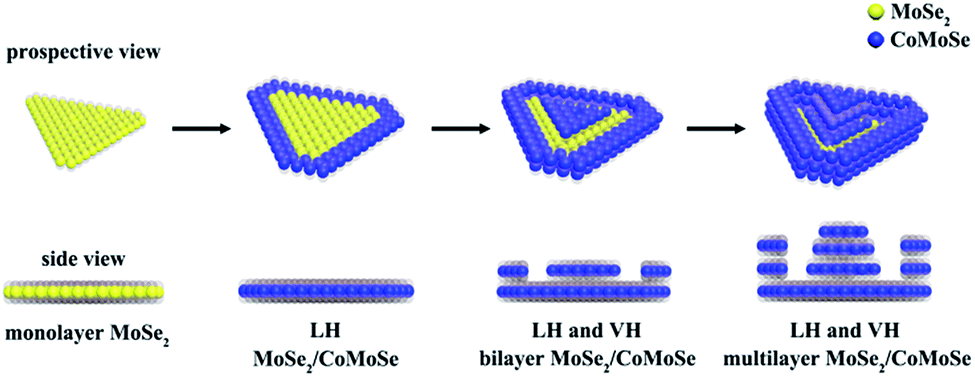 | ||
| Fig. 1 Schematic illustrations of the formation of defective 2D terrace MoSe2/CoMoSe LH and LH and VH nanolayers. | ||
Optical images in Fig. 2a and b display hexagonal MoSe2/CoMoSe LH nanolayers with dimensions ranging from ∼15 μm to 100 μm. The optical image (Fig. 2b) clearly reveals the MoSe2/CoMoSe LH through optical contrast diversity, with triangular MoSe2 monolayers displaying a pink color and CoMoSe alloy nanolayers, a purple color. The CoMoSe alloy nanolayers were grown along the MoSe2 triangle margins at ∼900 °C for 10 min to produce hexagonal MoSe2/CoMoSe LH nanolayers. However, the smaller optical image hardly shows the existence of the MoSe2/CoMoSe LH, due to less CoMoSe alloys along the edges of the triangular MoSe2. Fig. 2c exhibits bilayer (blue color in the middle) and multilayer (light white color in the middle) MoSe2/CoMoSe LH and VH optical images with a dimension of ∼15 μm. Low magnification SEM images (Fig. 2d and f) of MoSe2/CoMoSe LH and bilayer or multilayer LH and VH nanolayers measuring ∼15 μm are consistent with the results of the optical images. Individual high magnification SEM images of MoSe2/CoMoSe LH and bilayer or multilayer LH and VH nanolayers are shown in Fig. 2e, g, and f with different grayscale contrasts, respectively. Fig. 2i shows the Raman mapping image of 2D MoSe2/CoMoSe LH with the A1g characteristic peak of MoSe2. The edge of CoMoSe alloy demonstrates a weaker intensity of A1g Raman peak than that in the center of MoSe2 because of the Co doping in the margin of MoSe2/CoMoSe LH nanolayers.
 | ||
| Fig. 2 Optical, SEM, and Raman mapping of defective 2D terrace MoSe2/CoMoSe LH and LH and VH nanolayers. (a and b) Optical images of 2D MoSe2/CoMoSe LH nanolayers. (c) Optical image of 2D MoSe2/CoMoSe LH and VH nanolayers. (d and e) SEM images of 2D MoSe2/CoMoSe LH nanolayers. (f–h) SEM images of 2D MoSe2/CoMoSe LH and VH nanolayers. (i) Raman mapping of 2D MoSe2/CoMoSe LH nanolayers. | ||
Fig. 3a displays the Raman spectra of 2D LH center (MoSe2 region), LH edge (CoMoSe region), and bilayer and multilayer (MoSe2/CoMoSe) VH, which reveal two typical Raman characteristic peaks of MoSe2 at low wavenumber (A1g mode, out-plane vibration) and high wavenumber (E2g mode, in-plane vibration). The MoSe2 monolayer region exhibits the A1g mode at 240.3 cm−1 and the E2g mode at 288.2 cm−1, respectively. However, as the Co doping and thickness increase, the A1g mode displays a blue shift to high wavenumber side, suggesting the possible effects of Co doping and/or thickness variation on a 2D thin layer structure. According to the reports of the literatures, the Raman spectra of the hexagonal single-crystal MoS2 possess two major peaks E12g and A1g modes (which correspond to the vibrational motions of Mo and S atoms in the x–y layered plane and two S atoms along the z-axis of the unit cell, respectively). The exact peak positions depend on the layer thickness of the samples. As the thickness decreased, the frequencies of the E12g and A1g modes increased and decreased, respectively. These trends can be ascribed to the coulombic interactions and possible stacking-induced changes in the intralayer bonding.34,35 2D TMDCS MoSe2 and MoS2 materials have a very similar structure and both are assigned to the same kind of material. Therefore, the blue shift of the A1g mode in our samples may also be assigned to the thickness variation of the layer structure. With the increase of Co doping and the number of layers, the PL peak exhibits a red shift phenomenon. Generally, Raman and PL spectra indicate the high quality of the as-obtained atomic layers of 2D MoSe2/CoMoSe heterostructures.
 | ||
| Fig. 3 Raman, PL, and AFM characterization of defective 2D terrace MoSe2/CoMoSe LH and LH and VH nanolayers. (a) Raman and (b) PL spectra in 2D MoSe2/CoMoSe LH center, edge, bilayer, and multilayer MoSe2/CoMoSe VH. (c–e) AFM height and (f–h) the corresponding AFM phase images of 2D MoSe2/CoMoSe LH, bilayer, and multilayer MoSe2/CoMoSe LH and VH nanolayers. | ||
The thicknesses of 2D MoSe2/CoMoSe heterostructures are shown in Fig. 3c–e obtained using the AFM technique. The results exhibit that the interior MoSe2 is a monolayer of ∼0.7 nm and the CoMoSe alloy outside possesses a higher thickness of ∼1.8 nm (Fig. 3c) in the MoSe2/CoMoSe LH because Co doping can act as a metal catalyst and, hence, facilitate the growth rate of MoSe2 during the reaction process. Bilayer and multilayer MoSe2/CoMoSe LH and VH nanolayers with the heights of ∼1.4 nm (bilayer MoSe2/CoMoSe VH) and 18.9 nm (multilayer MoSe2/CoMoSe VH) are also shown in Fig. 3d and e, respectively. The AFM measurement results also show 2D terrace structural patterns with more edge layers. Fig. 3f–h display the corresponding AFM phase images of different types of MoSe2/CoMoSe heterostructures, demonstrating that distinct phases by the difference of the color contrast are in different regions with various (MoSe2 or CoMoSe) ingredients. These results further prove the successful doping of Co element in MoSe2 atomic layers.
The XRD pattern of 2D MoSe2/CoMoSe LH atomic layers (Fig. 4a, in dark) only displays a hexagonal structure of MoSe2 regardless of the Co composition, simply because the content of Co element is very low in the MoSe2/CoMoSe LH. However, the XRD pattern of the MoSe2/CoMoSe LH and VH atomic layers (Fig. 4a, in red) exhibits a hexagonal structure of MoSe2 and Co0.85Se, indicating the successful introduction of Co element into the MoSe2 thin layers. Fig. 4b–d exhibit the XPS spectra of the 2D MoSe2/CoMoSe LH (in black) and MoSe2/CoMoSe LH and VH (in red) atomic layers. The Mo 3d peaks (3d5/2, 228.3 eV; 3d3/2, 231.4 eV) and Se 3d peaks (3d5/2, 53.9 eV; 3d3/2, 54.7 eV) in Fig. 4b and d, respectively, are attributed to MoSe2 in accordance with the reported values.36,37 The Co 2p core-level peaks of Co2+ 2p3/2, Co3+ 2p3/2, Co2+ 2p1/2, and Co3+ 2p1/2 are located at ∼780.8, 779.0, 797.2, and 794.0 eV, respectively, as shown in Fig. 4c, which are close to the previous reports of Co0.85Se materials.38,39 The Co doping levels of 2D terrace MoSe2/CoMoSe LH and LH and VH nanolayers are 1.3 and 5.3 wt%, respectively. The Co content in MoSe2/CoMoSe LH is obviously lower than those in MoSe2/CoMoSe LH and VH. These results are consistent with the XRD results. The existence of Co 2p peaks in the products further manifest the successful Co doping in MoSe2 atom layers.
 | ||
| Fig. 4 XRD and XPS characterization of defective 2D terrace MoSe2/CoMoSe LH and LH and VH nanolayers. (a) XRD patterns, (b) Mo 3d, (c) Co 2p, and (d) Se 3d XPS spectra. | ||
For comparison, triangular MoSe2 monolayers (Fig. S2†) were also grown and characterized using various techniques. Fig. S2a† exhibits high density triangular MoSe2 with the size of ∼10 μm, which displays homogeneous color contrast in the optical image. Homogeneous color indicates the high quality crystal and uniform thickness of the grown MoSe2 triangles. These results are in agreement with the SEM image shown in Fig. S2b.† The thickness of MoSe2 triangles is ∼0.7 nm, indicating that the grown MoSe2 triangles are monolayers. The AFM phase image (the inset of Fig. S2f†) exhibits the single MoSe2 phase due to the same color contrast. The XPS spectra of Mo 3d (Fig. S2d†) and Se 3d (Fig. S2e†) and the Raman (Fig. S2g†) and PL (Fig. S2h†) spectra of MoSe2 triangles are consistent with the previous results of MoSe2 region in MoSe2/CoMoSe heterostructures. The Co 2p peaks are absent in Fig. S2f,† as expected. The schematic illustration of prospective and side views of triangular MoSe2 monolayers is shown in Fig. S2i.†
Different magnification TEM images of defective 2D terrace MoSe2/CoMoSe LH (Fig. 5a and d) and bilayer (Fig. 5b and e) and multilayer (Fig. 5c and f) MoSe2/CoMoSe LH and VH nanolayers clearly show the different types of MoSe2/CoMoSe heterostructures with diverse number of layers through contrasting the light and dark regions of the images. With the increase of the number of layers, the image color becomes darker. High magnification TEM image (Fig. 5f) of multilayer MoSe2/CoMoSe LH and VH nanolayers clearly displays the terrace structures of the products with more edge layers. The black nanoparticles in the TEM images are the residual impurities during the transfer procedure for the as-grown nanolayers from the SiO2/Si substrate to Cu TEM grid. The elemental composition obtained from the TEM-EDX characterization (Fig. S3†) of multilayer MoSe2/CoMoSe LH and VH in the thick core region exhibits the existence of Mo, Co, and Se elements in the products. The crystalline structure of 2D MoSe2/CoMoSe heterostructures was further investigated using SAED. All the SAED patterns in the regions of MoSe2 monolayer (Fig. 5g), bilayer MoSe2/CoMoSe VH (Fig. 5h), and multilayer MoSe2/CoMoSe VH (Fig. 5i) apparently display a single set of hexagonally arranged diffraction spots that can be attributed to the six-fold symmetry of the [001] zone axis of the MoSe2 lattice structure. These results reveal that there is no change of the crystalline structure of MoSe2, although the doping of the Co element into the MoSe2 atom layers results in the formation of the CoMoSe alloy. The HRTEM images in Fig. 5j–l show a lattice plane spacing of 0.28 nm that can be assigned to the (100) plane of MoSe2, which is consistent with the previous reports.5,40 It is worth noting that slight atomic arrangement distortions and point defects are observed and marked with the red circles in Fig. 5k, l and S4† in some regions of the HRTEM images of MoSe2/CoMoSe heterostructures (dark circles display the perfect crystal structure (nondefect form)), which still preserve the pristine 2D MoSe2 crystalline arrangement. Slight distortions and point defects in the basal plane of 2D TMDCS atomic layers will generate more active sites to activate the inert 2D basal plane for improving the HER activity, since the active sites of perfect 2D TMDCS atomic layers only exist at the edges. The corresponding schematic illustration is shown in Fig. S5.†
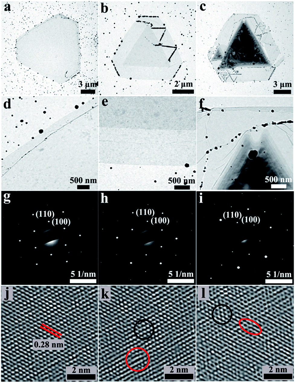 | ||
| Fig. 5 TEM characterization of defective 2D terrace MoSe2/CoMoSe LH and LH and VH nanolayers. Different magnification TEM images, SAED patterns, and HRTEM images of 2D MoSe2/CoMoSe LH (a, d, g and j), bilayer MoSe2/CoMoSe LH and VH (b, e, h and k), and multilayer MoSe2/CoMoSe LH and VH (c, f, i and l) nanolayers. | ||
Based on the successful heterogeneous doping of Co in the MoSe2 atomic layers, there could be more active sites to be produced due to the atomic distortion in the CoMoSe alloy nanolayers; therefore, it could be beneficial for HER applications to combine with Co catalysis. From the literature, the heterogeneous spin states lead to a distorted atomic arrangement, and the metal ions inserted into the TMDCS atomic layers provide the fresh desired nanomaterial for optimizing the HER active sites.15 Moreover, the formation of 2D TMDCS atomic layers is crucial for the primitive electron conjugated structure on the 2D plane and beneficial to fast electron transfer for optimizing the HER performance.15
In order to prove the above discussions, the electrocatalytic HER performance of defective 2D terrace MoSe2/CoMoSe LH and LH and VH nanolayers was investigated, and the results are shown in Fig. 6. The HER measurements were performed in a three-electrode system with a 0.5 M H2SO4 solution. The 2D atomic layer products were transferred from the SiO2/Si substrate to the GC electrode using PMMA solution as the working electrode. A schematic diagram of the 2D atomic layer materials on the GC electrode is shown in Fig. 6a. The electrons are shifted from the GC electrode to the 2D atomic layer materials and finally acquired by hydrogen ions. The polarization curves for triangular MoSe2 monolayers, MoSe2/CoMoSe LH, and MoSe2/CoMoSe LH and VH nanolayers, along with those of commercial Pt/C (∼0.57 mg cm−2; Pt 10%, Aladdin) and bare GC electrode for comparison, are shown in Fig. 6b. All of the 2D TMDCS atomic layers exhibit low overpotentials to steer the electrode reaction: among them, MoSe2/CoMoSe LH and VH presents the lowest current density of 305 mV at 10 mA cm−2, suggesting the best HER activity. In contrast, triangular MoSe2 monolayers and MoSe2/CoMoSe LH displayed inadequate HER performance with larger overpotentials of 378 mV and 339 mV at 10 mA cm−2 current density, respectively. Tafel slope was used to further assess the HER activity of the products, which is a crucial parameter that exhibits hydrogen evolution reaction dynamics. As shown in Fig. 6c, the smallest Tafel slope of ∼95.2 mV dec−1 was calculated for the MoSe2/CoMoSe LH and VH, and the obtained value is clearly smaller than those of MoSe2/CoMoSe LH (∼122.3 mV dec−1) and triangular MoSe2 monolayers (∼134.2 mV dec−1). As far as we have searched in the literature, the HER activity of MoSe2/CoMoSe LH and VH is comparable to the most reported value from 2D noble-metal-free TMDCS atomic layer electrocatalysts (Table S1†).
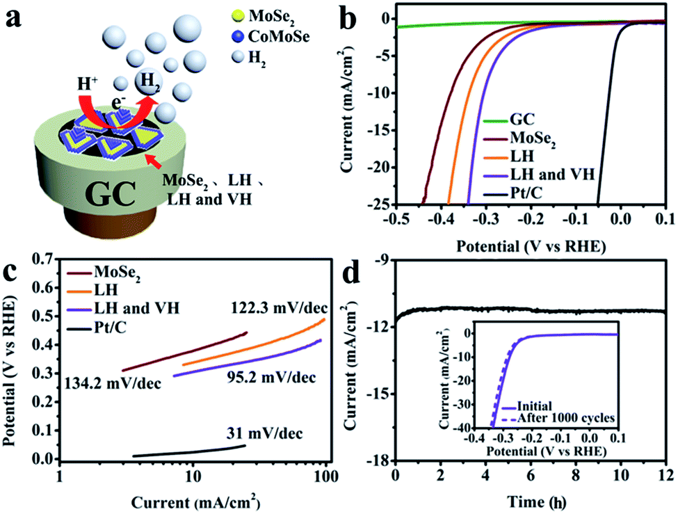 | ||
| Fig. 6 Electrochemical catalytic performance of 2D triangular MoSe2 monolayers, defective 2D terrace MoSe2/CoMoSe LH, and LH and VH nanolayers on GC electrode. (a) Schematic illustration, (b) polarization curves after iR correction, (c) Tafel plots, and (d) stability testing. | ||
The Nyquist plots (Fig. S6†) show that the charge-transfer resistances (Rct) of 2D triangular MoSe2 monolayers, defective 2D terrace MoSe2/CoMoSe LH, and LH and VH nanolayers are ∼239.7, 89.5, and 35.2 Ω at 310 mV overpotential (vs. RHE), respectively. The MoSe2/CoMoSe LH and VH nanolayers exhibit the lowest Rct; therefore, they are the best catalyst with the highest rate of charge transfer for all the products in this study. Apart from the HER activity and conductivity, the stability of the materials is also a significant factor for the best performance of the electrocatalyst. To confirm the long-term durability of MoSe2/CoMoSe LH and VH when preserved under a strong-acid condition, the MoSe2/CoMoSe LH and VH electrocatalyst was kept in 0.5 M sulfuric acid with an overpotential of 310 mV for 12 h and cycled for 1000 cycles. As shown in Fig. 6d, a minor degradation in the current density and overpotential after the stability test suggests that this electrocatalyst has excellent stability. Further, the microstructure of MoSe2/CoMoSe LH and VH catalyst after the long-term test has slightly altered, as shown in Fig. S7 and S8.†
Based on the electrocatalytic measurement, the combination of good electrocatalytic parameters of the small overpotential at 10 mA cm−2 current density, low Tafel slope, large current density, and good stability for the MoSe2/CoMoSe LH and VH electrocatalyst clearly proves that the formation of distorted atomic structures, 2D terrace edge layered architecture, and using more Co element catalyst in MoSe2/CoMoSe LH and VH enhance the additional HER activity sites and improve the HER performance.
Conclusions
In conclusion, defective 2D terrace MoSe2/CoMoSe LH and bilayer and multilayer MoSe2/CoMoSe LH and VH nanolayers have been successfully grown on SiO2/Si substrates using the CVD method. The Co element was inserted into MoSe2 atomic layers at a high temperature of ∼900 °C to fabricate CoMoSe nanolayers, and then the 2D MoSe2/CoMoSe LH and VH were obtained by the growth of CoMoSe alloy along the edge and on the surface of the MoSe2 monolayers. As a result of the heterogeneous doping of Co in MoSe2, more active sites were created through the atomic re-arrangement and distortion in the CoMoSe alloy thin layers, atomic level coarsening in LH abutments, and added terrace edge layers in VH enhancing the HER performance accompanying with metal Co element catalysis. 2D MoSe2/CoMoSe LH and VH nanolayers display the lowest overpotential (305 mV) at a current density of 10 mA cm−2, the smallest Tafel slope (95.2 mV dec−1), and good stability of the obtained devices under a strong-acid condition, which are comparable with those reported for 2D TMDCS thin layer materials. It is believed that the present method is a facile yet trustworthy technique to doping other metal ions into 2D TMDCS atomic layers to generate novel types of alloy nanolayers for obtaining new LH or VH on diverse substrates, and it can open our mind toward the development of the next generation of HER electrocatalysts.Acknowledgements
This work is supported by the National Natural Science Foundation of China (NSFC, no. 61172001, 61390502, and 21373068), and the National Key Basic Research Program of China (973 Program) under Grant no. 2013CB632900, and by the Foundation for Innovative Research Groups of the National Natural Science Foundation of China (Grant no. 51521003) and by Self-Planned Task (no. SKLRS201607B) of State Key Laboratory of Robotics and System (HIT), as well as the UK Engineering and Physical Sciences Research Council (EPSRC) EP/P018998/1, and Newton Mobility Grant (IE161019) through Royal Society and the NSFC.Notes and references
- M. Mahjouri-Samani, M. W. Lin, K. Wang, A. R. Lupini, J. Lee, L. Basile, A. Boulesbaa, C. M. Rouleau, A. A. Puretzky, I. N. Ivanov, K. Xiao, M. Yoon and D. B. Geohegan, Nat. Commun., 2015, 6, 7749 CrossRef CAS PubMed.
- W. Zheng, W. Feng, X. Zhang, X. S. Chen, G. B. Liu, Y. F. Qiu, T. Hasan, P. H. Tan and P. A. Hu, Adv. Funct. Mater., 2016, 26, 2648–2654 CrossRef CAS.
- X. S. Chen, G. B. Liu, W. Zheng, W. Feng, W. W. Cao, W. P. Hu and P. A. Hu, Adv. Funct. Mater., 2016, 26, 8537–8544 CrossRef CAS.
- W. Zheng, J. H. Lin, W. Feng, K. Xiao, Y. F. Qiu, X. S. Chen, G. B. Liu, W. W. Cao, S. T. Pantelides, W. Zhou and P. A. Hu, Adv. Funct. Mater., 2016, 26, 6371–6379 CrossRef CAS.
- X. D. Duan, C. Wang, J. C. Shaw, R. Cheng, Y. Chen, H. L. Li, X. P. Wu, Y. Tang, Q. L. Zhang, A. L. Pan, J. H. Jiang, R. Q. Yu, Y. Huang and X. F. Duan, Nat. Nanotechnol., 2014, 9, 1024–1030 CrossRef CAS PubMed.
- J. M. Woods, Y. Jung, Y. J. Xie, W. Liu, Y. H. Liu, H. H. Wang and J. J. Cha, ACS Nano, 2016, 10, 2004–2009 CrossRef CAS PubMed.
- H. Fang, C. Battaglia, C. Carraro, S. Nemsak, B. Ozdol, J. S. Kang, H. A. Bechtel, S. B. Desai, F. Kronast, A. A. Unal, G. Conti, C. Conlon, G. K. Palsson, M. C. Martin, A. M. Minor, C. S. Fadley, E. Yablonovitch, R. Maboudian and A. Javey, Proc. Natl. Acad. Sci. U. S. A., 2014, 111, 6198–6202 CrossRef CAS PubMed.
- D. Voiry, H. Yamaguchi, J. W. Li, R. Silva, D. C. B. Alves, T. Fujita, M. W. Chen, T. Asefa, V. B. Shenoy, G. Eda and M. Chhowalla, Nat. Mater., 2013, 12, 850–855 CrossRef CAS PubMed.
- B. L. Liu, Y. Q. Ma, A. Y. Zhang, L. Chen, A. N. Abbas, Y. H. Liu, C. F. Shen, H. C. Wan and C. W. Zhou, ACS Nano, 2016, 10, 5153–5160 CrossRef CAS PubMed.
- H. L. Li, Q. L. Zhang, X. D. Duan, X. P. Wu, X. P. Fan, X. L. Zhu, X. J. Zhuang, W. Hu, H. Zhou, A. L. Pan and X. F. Duan, J. Am. Chem. Soc., 2015, 137, 5284–5287 CrossRef CAS PubMed.
- Y. Liu, N. O. Weiss, X. D. Duan, H. C. Cheng, Y. Huang and X. F. Duan, Nat. Rev. Mater., 2016, 1, 16042 CrossRef CAS.
- L. Samad, S. M. Bladow, Q. Ding, J. Q. Zhuo, R. M. Jacobberger, M. S. Arnold and S. Jin, ACS Nano, 2016, 10, 7039–7046 CrossRef CAS PubMed.
- Q. Fu, L. Yang, W. H. Wang, A. Han, J. Huang, P. W. Du, Z. Y. Fan, J. Y. Zhang and B. Xiang, Adv. Mater., 2015, 27, 4732–4738 CrossRef CAS PubMed.
- X. S. Chen, Z. G. Wang, Y. F. Qiu, J. Zhang, G. B. Liu, W. Zheng, W. Feng, W. W. Cao, P. A. Hu and W. P. Hu, J. Mater. Chem. A, 2016, 4, 18060–18066 CAS.
- Y. W. Liu, X. M. Hua, C. Xiao, T. F. Zhou, P. C. Huang, Z. P. Guo, B. C. Pan and Y. Xie, J. Am. Chem. Soc., 2016, 138, 5087–5092 CrossRef CAS PubMed.
- Y. Zhang, X. S. Chen, Y. Huang, C. Zhang, F. Li and H. B. Shu, J. Phys. Chem. C, 2017, 121, 1530–1536 CAS.
- L. X. Lin, N. H. Miao, Y. Wen, S. W. Zhang, P. Ghosez, Z. M. Sun and D. A. Allwood, ACS Nano, 2016, 10, 8929–8937 CrossRef CAS PubMed.
- M. Mahjouri-Samani, L. B. Liang, A. Oyedele, Y. S. Kim, M. K. Tian, N. Cross, K. Wang, M. W. Lin, A. Boulesbaa, C. M. Rouleau, A. A. Puretzky, K. Xiao, M. Yoon, G. Eres, G. Duscher, B. G. Sumpter and D. B. Geohegan, Nano Lett., 2016, 16, 5213–5220 CrossRef CAS PubMed.
- X. F. Li, M. W. Lin, L. Basile, S. M. Hus, A. A. Puretzky, J. Lee, Y. C. Kuo, L. Y. Chang, K. Wang, J. C. Idrobo, A. P. Li, C. H. Chen, C. M. Rouleau, D. B. Geohegan and K. Xiao, Adv. Mater., 2016, 28, 8240 CrossRef CAS PubMed.
- H. J. Chuang, B. Chamlagain, M. Koehler, M. M. Perera, J. Q. Yan, D. Mandrus, D. Tomanek and Z. X. Zhou, Nano Lett., 2016, 16, 1896–1902 CrossRef CAS PubMed.
- X. S. Chen, Y. F. Qiu, H. H. Yang, G. B. Liu, W. Zheng, W. Feng, W. W. Cao, W. P. Hu and P. A. Hu, ACS Appl. Mater. Interfaces, 2017, 9, 1684–1691 CAS.
- J. Staszak-Jirkovsky, C. D. Malliakas, P. P. Lopes, N. Danilovic, S. S. Kota, K. C. Chang, B. Genorio, D. Strmcnik, V. R. Stamenkovic, M. G. Kanatzidis and N. M. Markovic, Nat. Mater., 2016, 15, 197–204 CrossRef CAS PubMed.
- N. Kornienko, J. Resasco, N. Becknell, C. M. Jian, Y. S. Liu, K. Q. Nie, X. H. Sun, J. H. Guo, S. R. Leone and P. D. Yang, J. Am. Chem. Soc., 2015, 137, 7448–7455 CrossRef CAS PubMed.
- Y. Ito, W. T. Cong, T. Fujita, Z. Tang and M. W. Chen, Angew. Chem., 2015, 54, 2131–2136 CrossRef CAS PubMed.
- X. D. Yan, L. H. Tian, M. He and X. B. Chen, Nano Lett., 2015, 15, 6015–6021 CrossRef CAS PubMed.
- D. S. Kong, H. T. Wang, Z. Y. Lu and Y. Cui, J. Am. Chem. Soc., 2014, 136, 4897–4900 CrossRef CAS PubMed.
- G. B. Liu, Z. H. Li, T. Hasan, X. S. Chen, W. Zheng, W. Feng, D. C. Jia, Y. Zhou and P. A. Hu, J. Mater. Chem. A, 2017, 5, 1989–1995 CAS.
- Y. Li, L. Zhang, X. Xiang, D. P. Yan and F. Li, J. Mater. Chem. A, 2014, 2, 13250–13258 CAS.
- L. Zhang, W. H. He, X. Xiang, Y. Li and F. Li, RSC Adv., 2014, 4, 43357–43365 RSC.
- W. H. He, R. R. Wang, L. Zhang, J. Zhu, X. Xiang and F. Li, J. Mater. Chem. A, 2015, 3, 17977–17982 CAS.
- J. P. Shi, D. L. Ma, G. F. Han, Y. Zhang, Q. Q. Ji, T. Gao, J. Y. Sun, X. J. Song, C. Li, Y. S. Zhang, X. Y. Lang, Y. F. Zhang and Z. F. Liu, ACS Nano, 2014, 8, 10196–10204 CrossRef CAS PubMed.
- Y. F. Yu, S. Y. Huang, Y. P. Li, S. N. Steinmann, W. T. Yang and L. Y. Cao, Nano Lett., 2014, 14, 553–558 CrossRef CAS PubMed.
- L. Yang, Q. Fu, W. H. Wang, J. Huang, J. L. Huang, J. Y. Zhang and B. Xiang, Nanoscale, 2015, 7, 10490–10497 RSC.
- W. Park, J. Baik, T. Y. Kim, K. Cho, W. K. Hong, H. J. Shin and T. Lee, ACS Nano, 2014, 8, 4961–4968 CrossRef CAS PubMed.
- C. Lee, H. Yan, L. E. Brus, T. F. Heinz, J. Hone and S. Ryu, ACS Nano, 2010, 4, 2695–2700 CrossRef CAS PubMed.
- G. W. Shim, K. Yoo, S. B. Seo, J. Shin, D. Y. Jung, I. S. Kang, C. W. Ahn, B. J. Cho and S. Y. Choi, ACS Nano, 2014, 8, 6655–6662 CrossRef CAS PubMed.
- X. L. Wang, Y. J. Gong, G. Shi, W. L. Chow, K. Keyshar, G. L. Ye, R. Vajtai, J. Lou, Z. Liu, E. Ringe, B. K. Tay and P. M. Ajayan, ACS Nano, 2014, 8, 5125–5131 CrossRef CAS PubMed.
- Z. X. Zhang, X. W. Wang, K. L. Wu, Y. X. Yue, M. L. Zhao, J. Cheng, J. Ming, C. J. Yu and X. W. Wei, New J. Chem., 2014, 38, 6147–6151 RSC.
- Z. H. Wang, Q. Sha, F. W. Zhang, J. Pu and W. Zhang, CrystEngComm, 2013, 15, 5928–5934 RSC.
- J. Xia, X. Huang, L. Z. Liu, M. Wang, L. Wang, B. Huang, D. D. Zhu, J. J. Li, C. Z. Gu and X. M. Meng, Nanoscale, 2014, 6, 8949–8955 RSC.
Footnote |
| † Electronic supplementary information (ESI) available. See DOI: 10.1039/c7ta02327h |
| This journal is © The Royal Society of Chemistry 2017 |