A type-II GeSe/SnS heterobilayer with a suitable direct gap, superior optical absorption and broad spectrum for photovoltaic applications
Congxin
Xia
 *a,
Juan
Du
a,
Wenqi
Xiong
a,
Yu
Jia
b,
Zhongming
Wei
 c and
Jingbo
Li
c
aCollege of Physics and Material Science, Henan Normal University, Xinxiang 453007, China. E-mail: xiacongxin@htu.edu.cn
bKey Laboratory for Special Functional Materials of Ministry of Education, Henan University, Kaifeng 475004, China
cInstitute of Semiconductors, Chinese Academy of Sciences, Beijing 100083, China
First published on 27th April 2017
Abstract
Van der Waals (vdW) heterobilayers are emerging as unique structures for next-generation electronic and optoelectronic devices. In this work, we predict that the GeSe/SnS heterobilayer has a direct band structure with a gap value of about 1.519 eV and typical type-II band alignment. Moreover, it possesses the characteristics of superior optical absorption (∼105) and a broad absorption spectrum from the visible light to the near ultraviolet region. In addition, the GeSe/SnS heterobilayer also exhibits obviously anisotropic electronic transport and optical properties with larger current and stronger optical absorption along the zigzag direction. Meanwhile, interlayer coupling and applying an external electric field are identified to be effective methods to modify its electronic and optical properties. Thus, these predicted results indicate that the GeSe/SnS heterobilayer will have promising applications in photovoltaic devices.
1. Introduction
In recent years, more and more two-dimensional (2D) nanomaterials have been attracting tremendous attention due to their novel properties, originating from quantum size effects and special structure characteristics, and they have also been applied successfully in nanoelectronics and optoelectronic devices, such as photodetectors1,2 and field-effect transistors.3–7 Nevertheless, studies show that no single 2D material possesses perfect properties for practical applications. For example, the zero band gap of graphene limits its optoelectronic applications.8,9 Thus, the modulation of electronic structures and properties is always an open question for the studies of 2D nanomaterials by using doping, strain and electric field. Among these used methods, constructing van der Waals (vdW) heterobilayers is intensely carried out to combine together the advantages of building monolayers in experiment and theory.10–14More recently, another kind of 2D nanomaterial, group-IV monochalcogenides (SnS, SnSe, GeS and GeSe), has been attracting considerable attention because they possess puckered structures similar to that of phosphorene, displaying obvious anisotropic characteristics.15,16 Moreover, they are earth-abundant and environmentally friendly materials with suitable band gap values (1.1–1.5 eV) and superior photovoltaic performances.17–19 As prototypes, 2D SnS and GeSe materials have been identified to have promising applications in optoelectronic devices. For 2D GeSe, the fundamental band gap is found to be direct and it also possesses a small carrier effective mass. In addition, 2D SnS nanosheets also possess obviously anisotropic electronic characteristics and they can be tuned effectively by strain20 and layer numbers.21 Moreover, 2D SnS and GeSe monolayers are intrinsic multiferroic materials with coupled ferroelectricity and ferroelasticity at room temperature, which is useful for potential applications in information storage.22–24 The exciton binding energy was investigated theoretically in 2D GeS and GeSe monolayers.25 In experiments, SnS and GeSe 2D atomic crystals were also fabricated by using liquid-phase exfoliation.26 These studies show that 2D SnS and GeSe materials are considered to be promising alternative materials for optoelectronic applications.
In this work, we focus on the study of the 2D GeSe/SnS vdW heterobilayer due to its special optoelectronic properties and the good lattice match between monolayer GeSe and SnS. Meanwhile, we also consider whether the electronic, optical and transport properties of the GeSe and SnS vdW heterobilayer can be effectively modulated by an external strain and electric field (E-field). Our calculations show that the GeSe/SnS heterobilayer possesses not only typical type-II band alignment and a direct gap of 1.519 eV, but also obvious anisotropic characteristics and superb optical absorption, which indicates that it can become a promising candidate for applications in photovoltaic devices.
2. Computational methods
In the present simulations, first-principles calculations are performed based on the density functional theory (DFT) using the projector-augmented wave (PAW) method as implemented in the Vienna ab initio simulation package (VASP).27–29 The exchange-correlation functional is treated within the generalized gradient approximation (GGA) and parameterized using the Perdew–Burke–Ernzerhof (PBE) formula.30 For the vdW interaction in the GeSe/SnS heterobilayer, the DFT-D2 method of Grimme is used. As the DFT method is known to underestimate the band gap of semiconductors, thus accurate calculations are always required to correct the gap values, such as Heyd–Scuseria–Ernzerhof (HSE) and GW methods. Moreover, previous studies show that HSE methods give lower band gaps than GW calculations for 2D materials.31 However, GW calculations are more computationally expensive than HSE methods. Thus, the band structures and optical properties of GeSe/SnS heterobilayers are calculated by using the HSE06 methods in this work.32,33 In addition, a plane wave basis set with a cutoff energy of 500 eV and a 21 × 21 × 1 k-point grid determined by the gamma-centered Monkhorst–Pack method in the Brillouin zone is found to give good converged results.34 The atomic structures are relaxed until the forces on all unconstrained atoms are smaller than 0.01 eV Å−1 and the total energy convergence criterion is chosen as 10−5 eV. Moreover, a vacuum region of 20 Å along the z direction is used to avoid spurious interaction due to the non-local nature of the correlation energy. For the study of optical properties, the optical absorption coefficient α(ω) can be obtained by using the formula , in which ε1(ω) and ε2(ω) denote the real part and imaginary part of the complex dielectric function. In addition, the transport properties are calculated within the framework of density functional theory (DFT) combined with the non-equilibrium Green's function method (NEGF) as implemented in Atomistix ToolKit (ATK).35–38 A double-ζ polarized (DZP) basis set was used for the electron wave function. A mesh cutoff energy of 150 Ry and a Monkhorst–Pack k-mesh of 1 × 100 × 100 are employed in the transport property calculations.
3. Results and discussion
3.1 Structural and electronic properties of GeSe and SnS monolayers
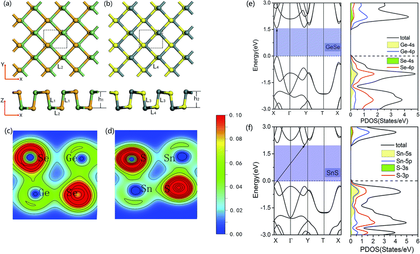
To construct the theoretical model of the 2D GeSe/SnS vdW heterobilayer, we first discuss the geometric parameters of the individual GeSe and SnS monolayers. For the GeSe monolayer, the optimized lattice constants are a = 4.28 Å and b = 3.97 Å, the buckling height h1 = 2.60 Å, and the Ge–Se bond lengths are L1 = 2.54 Å and L2 = 2.66 Å, as shown in Fig. 1a, which agree well with the values reported by other research groups.39–41 Meanwhile, for the SnS monolayer, it can be seen from Fig. 1b that the lattice constants are a = 4.25 Å and b = 4.08 Å, the buckling height h2 = 2.84 Å, and the Sn–S bond lengths are L3 = 2.59 Å and L4 = 2.74 Å, which are also consistent with previous studies.39–41In order to reveal the characteristics of bonding in the monolayer GeSe and SnS, Fig. 1c and d further present the charge density of GeSe and SnS unit cells. There is obvious overlap of electron densities between Ge(Sn) and Se(S) atoms, which suggests the formation of covalent bonding in the 2D GeSe and SnS nanosheets. In addition, Bader charge analysis is also performed to quantify the charge transfer, showing that each Ge atom donates 0.66e per Se atom in the GeSe monolayer, while each Sn atom donates 0.95e per S atom in the SnS monolayer. Moreover, because Se(S) atoms have larger electronegativity than Ge(Sn) atoms, we can conclude that charges tend to transfer to the atom with larger electronegativity.
In Fig. 1e and f, we further present the band structures and projected density of states (PDOS) of the monolayer GeSe and SnS unit cells. Our calculations show that the GeSe monolayer is a direct band gap semiconductor with a value of 1.602 eV, in which both the valence band maximum (VBM) and the conduction band minimum (CBM) reside at the same high-symmetry point in the Brillouin zone (BZ). In addition, as shown in Fig. 1e, for the GeSe monolayer, the states in the VBM are comprised of Se-4p and 4s and 4p states of Ge atoms, while the CBM is mainly contributed by the 4p states of Ge atoms and 4s and 4p states of Se atoms. In contrast to the GeSe monolayer, Fig. 1f shows that in the band structures of the SnS monolayer, the VBM lies along the Γ–X line, while its CBM resides along the Γ–Y line in the BZ, showing that it is an indirect band gap semiconductor with a value of 2.036 eV. Moreover, the VBM of the SnS monolayer is contributed by the hybridization of the 3p states of S atoms and 5s and 5p states of Sn atoms, while the CBM is mainly contributed by the Sn-5p state, as can be seen in Fig. 1f.
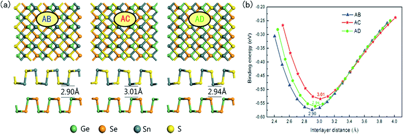
3.2 Structural and electronic properties of the GeSe/SnS heterobilayer
Now we construct the 2D GeSe/SnS vdW heterobilayer by attaching the GeSe and SnS monolayers together. Here the GeSe and SnS layers are stacked onto each other along the quasi-1D chain direction. Owing to their close lattice constants, the heterobilayer is built by their unit cells containing eight atoms in total, which induces a very small lattice mismatch. In the following, to get a comprehensive understanding, we consider three possible stacking patterns labeled AB, AC and AD in Fig. 2. For the AB pattern, the top layer SnS is directly stacked on the bottom GeSe monolayer. The AC pattern can be obtained by flipping the SnS monolayer of the AB pattern vertically by 180°, in which the top and bottom layers are mirror images of each other. Also, the AD pattern is constructed by shifting the top layer of the AC-stacking by half of the cell along the armchair direction.Note that twist angle effects are not considered in our calculations, which is similar to previous studies on vdW heterostructures.10–14 However, rotation may exist between the two isolated layers in some experiments. For example, Koda et al. have proved that interlayer twist angles play a role in the physics of vdW heterostructures.42 The twist angle can affect the physical behavior in terms of the changing interlayer separation and the character of the wave functions in different parts of the Brillouin zone. Generally speaking, the changed physical behavior via rotational stacking can be attributed to the interlayer interaction, and further the charge-transfer-induced strain. Detailed analyses of the effect of twisting on the electronic properties of van der Waals heterostructures have been reported by Jin and van der Zande et al.43,44 Thus, in our future research, we will work hard on the twist angle effects on the electronic structures of the GeSe/SnS heterobilayer.
In order to assess the relative stability of the heterobilayer, we calculate the binding energy (Eb) using the formula
| Eb = Eheterostructure − EGeSe − ESnS | (1) |
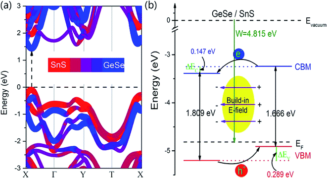
In order to understand clearly the electronic properties of the GeSe/SnS heterobilayer, the projected band structure is shown in Fig. 3a. It is found that the GeSe/SnS heterobilayer exhibits semiconducting characteristics with a direct band gap of 1.519 eV, in which both the CBM and VBM lie along the X–Γ line. In our case, the lowest conduction band mainly consists of the p orbitals of Ge, while the p orbitals of S contributed most to the topmost valence bands. To be precise, the CBM is composed of about 10% SnS and 90% GeSe, while the VBM is formed by about 91% SnS and 9% GeSe. We can also see from Fig. 3a that the CBM of the SnS layer is lower than that of the GeSe layer, whereas the VBM of the GeSe layer is higher than that of the SnS layer, which indicates that the excited electrons and holes are confined in different layers and leads to the formation of spatially indirect excitons, facilitating the effective separation of photogenerated holes and electrons. Furthermore, Fig. 3b also shows the band alignment of the GeSe/SnS heterobilayer using the vacuum level (Evacuum) as a common energy reference, which is significantly important in designing new materials and devices. This band alignment further demonstrates the type-II nature of the GeSe/SnS heterobilayer. Moreover, band offsets are crucial factors for its application in optoelectronic devices. Thus, we calculate the band offsets ΔEc and ΔEv of the isolated layers before contact (natural band offsets) and the heterobilayer after contact. The natural band offsets are calculated to be ΔEc = 0.297 eV and ΔEv = 0.135 eV, while the calculated band offsets of the heterobilayer are ΔEc = 0.147 eV and ΔEv = 0.289 eV. The difference of the band offsets before and after contact is mainly caused by the charge transfer between the GeSe and SnS layers in the heterobilayer. Similar behaviors can also be found in the hBN/MoSe2 heterobilayer systems.42
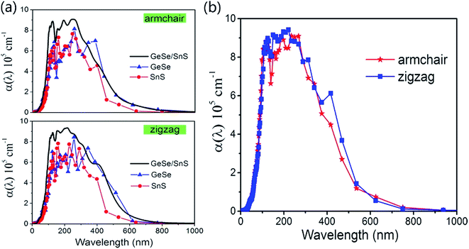
To explore the potential applications of the 2D GeSe/SnS heterobilayer in optoelectronic nano-devices, in Fig. 4 we further calculate the optical absorption coefficient α(ω) of the GeSe/SnS heterobilayer and the isolated GeSe and SnS layers along the armchair and zigzag directions. As seen from the figure, the heterobilayer exhibits a broad optical absorption range from the visible light to the ultraviolet light region, and the optical absorption intensity can reach the order of 105. The physical origin is given as follows. For isolated GeSe and SnS monolayers, their intrinsic superior optical absorbances are attributed to the nature of the atomic orbitals that form the band extrema of these materials. GeSe and SnS layers possess a larger number of bands that occur near the band extrema and larger joint density of states, thus resulting in a larger probability of optical transitions across the gap, as mentioned in the report by Shi et al.45 Moreover, compared with the isolated GeSe and SnS layers, the optical absorption is clearly enhanced in the heterobilayer in the ultraviolet light region. The behavior of improving optical absorption by constructing a heterobilayer can also be observed in other 2D vdW heterostructures.46,47 Moreover, the optical absorbance along the zigzag direction is stronger than that along the armchair direction in the visible light region. This anisotropic characteristic indicates that the GeSe/SnS heterobilayer can be used for developing polarized optical sensors. Thus, based on the physical analysis of Fig. 3 and 4, we can conclude that the GeSe/SnS heterobilayer possesses a typical type-II band alignment and has a direct gap value of 1.519 eV, which indicates that the lowest-energy electron–hole pairs can be spontaneously separated, consequently making the GeSe/SnS heterobilayer a good candidate for applications in photovoltaic devices. Moreover, the strong optical absorbance intensity and wide optical absorption, ranging from the visible light to the ultraviolet light region, will facilitate the application of the GeSe/SnS heterobilayer in the field of electrophotonic detectors.
To further understand the underlying physical mechanism of the electronic properties of the GeSe/SnS heterobilayer, we employ the z-direction planar-averaged charge density difference as depicted in Fig. 5. As is known to all, the charge redistribution behaviors, including the charge depletion (marked in blue) and charge accumulation (marked in red), lead to the polarization of electrons and the formation of an interface dipole. Also, the interface charge depletion is direct evidence of the surface charge repulsion effect, which easily causes surface orbital rehybridization. Thus, the integral of electron distribution indicates that electrons transfer from the SnS layer to the GeSe layer across the interface, which is also in accordance with the band alignment shown in Fig. 3b. Moreover, we also carry out the Bader charge analysis, suggesting that 0.016 electrons transfer from the SnS layer to the GeSe layer, and thereby the holes remained in the SnS layer. Accordingly, the SnS layer gathers positive charges and the GeSe layer accumulates negative charges. This charge distribution induces a built-in E-field in the heterobilayer system, which will hinder the diffusion of electrons and holes and the system will finally achieve balance with the diffusion force.
3.3 Interlayer coupling and electric field modulations of the electronic structures in the GeSe/SnS heterobilayer
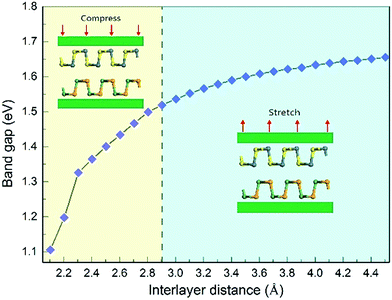
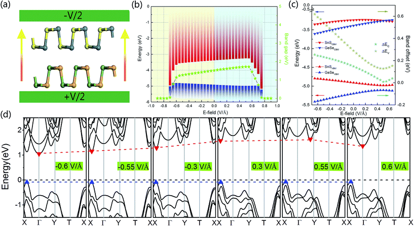
In order to study the effects of interlayer coupling on the electronic structures of the GeSe/SnS heterobilayer, the band gap as a function of the interlayer distance is shown in Fig. 6. It shows that when the compressive strain is exerted on the heterobilayer, a smaller interlayer distance is induced and the band gap exhibits a decreasing trend; in contrast, when a stretch strain is applied, resulting in a larger interlayer distance, the band gap increases. The reason is given as follows. The smaller interlayer distance leads to a stronger interaction in the heterobilayer, and thus results in more charge transfer. This can be verified by the plane-averaged charge density difference of the GeSe/SnS heterobilayer with three different interlayer distances, 2.4 Å, 2.9 Å and 3.4 Å, as shown in Fig. 5, showing that more charge accumulation/depletion can be found in the heterobilayer with a smaller interlayer distance. Moreover, Bader charge analysis also shows that there are 0.028, 0.016 and 0.009 electrons transferred from the SnS layer to the GeSe layer with interlayer distances of 2.4 Å, 2.9 Å and 3.4 Å, respectively. Thus, more charge transfer can induce a higher built-in E-field, which will reduce the band gap of the heterobilayer. This result also offers a possible way to modify the band gap by tuning the interlayer coupling of the vdW heterobilayer.Many research studies show that applying an external E-field is an effective way to tune the electronic properties of vdW heterobilayers.48–53 Thus, it is necessary to explore the E-field effects on the electronic properties of the GeSe/SnS heterobilayer, considering two directions (+z and −z) perpendicular to the stacking layers. And the positive direction of the external E-field is defined as pointing from the bottom GeSe layer to the upper SnS layer, as can be seen in Fig. 7a. The band gap of the GeSe/SnS heterobilayer as a function of the external E-field is plotted in Fig. 7b. Our results show that the changing trend of the band gap relies not only on the intensity but also on the direction of the external E-field. When the external E-field is applied along the +z direction, the band gap first increases, and then decreases rapidly when the E-field strength is beyond 0.5 V Å−1. However, when the E-field is applied along the −z direction, the band gap retains the monotonously decreasing trend as the strength of the E-field increases. Moreover, metallic properties can also be obtained when the intensity of the positive (negative) E-field is larger than 0.75(0.7) V Å−1. This large-scale band gap modulation indicates that applying an E-field can offer effective dynamic control over the band structures and optoelectronic properties of GeSe/SnS heterobilayer-based optoelectronic nano-devices.
In addition, Fig. 7b also shows that the asymmetric variation of the band gap with respect to the two opposite directions of the external E-field is the result of the interaction between the built-in E-field and applied external E-field. The reason can be given as follows. The direction of the positive external E-field is opposite to that of the built-in E-field. Thus, when the external E-field is applied at the beginning, the total E-field is decreased and the band gap is increased. However, when the strength of the positive external E-field reaches a certain value, the effect of built-in E-field is canceled out completely, and then further increase in the external E-field strength can result in the decrease of the band gap. In addition, as the direction of the negative external E-field is the same as that of the built-in E-field, the negative external E-field can increase the effect of built-in E-field. Thus, the application of the negative external E-field can monotonously decrease the band gap. This direction-dependent response of the external E-field can distinguish the GeSe/SnS heterobilayer from other non-polar structures.
To further explore the mechanism of the variation of the band gap under an external E-field, in Fig. 7b we exhibit the band edges under different external E-fields. It can be seen that the CBM of the heterobilayer increases first and then drops with increasing applied external E-field, and the changing trend is consistent with that of the band gap. However, the VBM of the heterobilayer does not show obvious changes under different external E-fields. So we can conclude that the increasing (decreasing) band gap is mainly caused by the up(down)-shift of the CBM, and the energy level of the VBM is insensitive to the intensity and direction of the E-field. Moreover, we present the band structures of the GeSe/SnS heterobilayer under different external E-fields in Fig. 7d. We can see that the external E-field affects obviously the energy level and the corresponding k-point position of the CBM. When the strength of the external E-field is smaller than 0.55 V Å−1, the CBM is retained along the X–Γ line, and the energy gap and band edge exhibit a continuously changing trend. However, when the strength of the external E-field exceeds 0.55 V Å−1, the CBM transfers first to the point along the Γ–Y line and then lies at the Γ point, and the energy level downshifts apparently. Therefore, an abrupt change in the energy gap and band edge is obtained. In addition, the band alignment and band offset of the GeSe/SnS heterobilayer as a function of the external E-field are plotted in Fig. 7c. In the case of the negative E-field, electrons transfer from the GeSe to the SnS layer, resulting in the bands of the GeSe layer moving downward, while the bands of the SnS layer move upward. Thus, the band offsets ΔEc and ΔEv are both enlarged under the negative E-field. However, the direction of the applied positive E-field is opposite to that of the built-in E-field, and therefore, electrons first transfer from the SnS to the GeSe layer under a relatively small external E-field, shifting the bands of the SnS layer downward and the bands of the GeSe layer upward. Further enhancement of the external E-field strength will cause electron transfer from the GeSe to the SnS layer, and opposite band shifting trends occur. Thus, the band offsets first decrease and then increase with increasing positive external E-field. The band shift is caused by the charge redistribution under different external E-fields, which can be interpreted as a bias in the Fermi level on each side of the interface. Similar behaviors can be found in phosphorene/MoSe2(WSe2) heterobilayers.54 Based on the above analyses, we can conclude that the band offset of the GeSe/SnS heterobilayer can be tuned effectively by an external E-field.
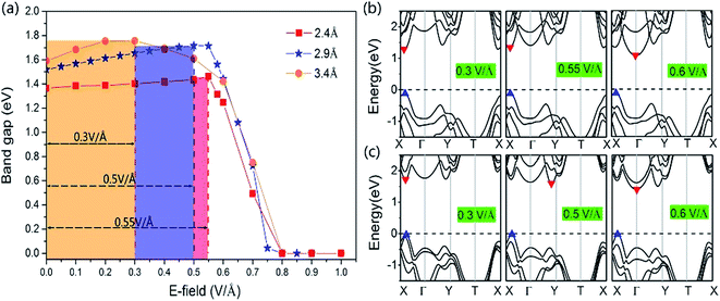
More interesting results with the GeSe/SnS heterobilayer can be found under the positive external E-field by changing the interlayer distance. We show the effect of the positive external E-field on the band gap with different interlayer distances, 2.4 Å and 3.4 Å, in Fig. 8. For comparison, the variation of the band gap under the positive external E-field with an equilibrium interlayer distance of 2.9 Å is also added to Fig. 8. These three systems exhibit similar trends. The band gap first increases as the intensity of the positive external E-field increases, and when the E-field reaches a certain value, the band gap decreases rapidly with increasing E-field intensity and finally becomes zero under a relatively large E-field intensity. The only difference is the turning point when the band gap begins to decrease. The turning point decreases with increasing interlayer distance. According to our results, the external E-field at the turning point corresponds to the built-in E-field intensity that needs to be canceled out for the heterobilayer. Thereby, we can verify the conclusion that the built-in E-field decreases with increasing interlayer distance. Our results show that not only the magnitude but also the direction of the external E-field could be utilized to manipulate the band gap of the GeSe/SnS heterobilayer. Moreover, the electronic band gap exhibits a rich behavior depending on both the interlayer distance and external E-field. The band structures of the GeSe/SnS heterobilayer under certain E-fields with interlayer distances of 2.4 Å and 3.4 Å are shown in Fig. 8b and c. The CBM of the heterobilayer under different E-fields also exhibits similar behaviors to those of the heterobilayer with an equilibrium interlayer distance of 2.9 Å, as shown in Fig. 7d.
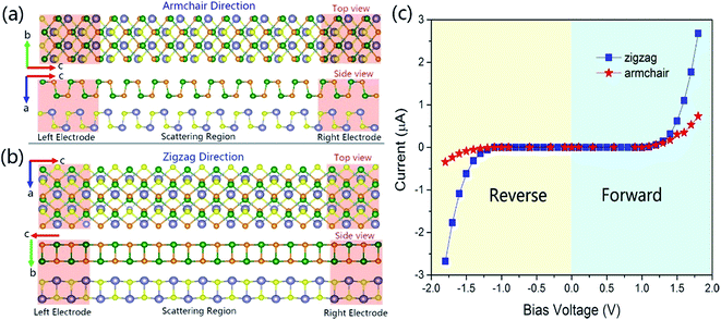
To calculate the electronic transport properties of the GeSe/SnS heterobilayer, two probe systems are constructed and shown in Fig. 9a and b. Here the system consists of three regions, two electrodes and a scattering region, where each electrode is modeled using a 2 × 2 supercell of the GeSe/SnS heterobilayer, and the length of the scattering region along the armchair direction and the zigzag direction is eight unit cell lengths. Moreover, the I–V curves are obtained by applying both forward and reverse bias voltages in the GeSe/SnS heterobilayer-based transport devices, which are shown in Fig. 9c. The current can be calculated using the relationship55
3.4 Electric field and interlayer coupling effects on the optical properties of the GeSe/SnS heterobilayer
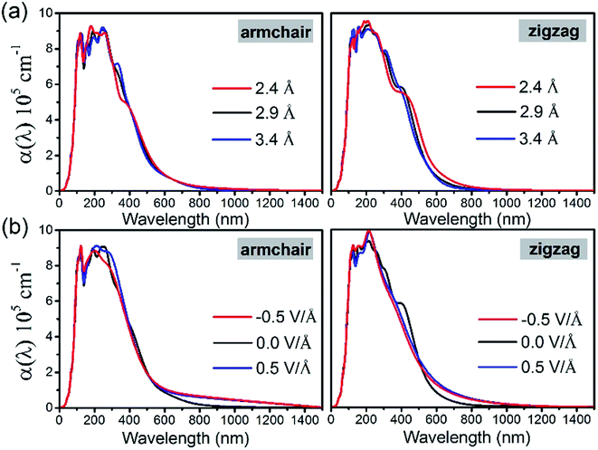
Now we investigate the interlayer coupling influences on the optical properties of the GeSe/SnS heterobilayer. In Fig. 10a, we present the optical absorption coefficient α(λ) of the GeSe/SnS heterobilayer with different interlayer distances 2.4 Å, 2.9 Å and 3.4 Å, along the armchair and zigzag directions. The results show that the optical anisotropy can also be found for different interlayer distances with stronger optical absorption in the visible light region along the zigzag direction. Interestingly, we find that the optical absorption along the armchair direction is insensitive to the interlayer coupling in the visible light region, but sensitive in the near ultraviolet region, and a weaker coupling may cause a stronger optical absorption. However, the optical absorption along the zigzag direction is sensitive to the interlayer coupling both in the near ultraviolet region and in the visible light region. And a weaker coupling can result in a stronger optical absorbance in the near ultraviolet region but a weaker optical absorbance in the visible light region. Thus, these results show that the interlayer coupling modulation can be helpful to the visible light applications of GeSe/SnS heterobilayers.The effects of external E-field on the optical properties are also studied with the selected E-field strength of 0.5 V Å−1 in two directions (+z and −z) considering the anisotropy along the armchair and zigzag directions, as shown in Fig. 10b. The results show that the optical absorption along the armchair direction is modified in both the near ultraviolet region and the near-infrared region, while the optical absorption along the zigzag direction is obviously tuned in the visible light region despite the direction of the external E-field. Interestingly, anisotropic optical absorption along the armchair and zigzag directions is also observed. The E-field has no effect on the visible light absorption along the armchair direction of the GeSe/SnS heterobilayer, but has some influence on that along the zigzag direction. Moreover, relatively stronger optical absorption in the visible light region can be found along the zigzag direction. Thus, we can conclude that an external E-field can be used effectively to tune the optical properties of the GeSe/SnS heterobilayer.
4. Conclusion
In summary, based on the vdW corrected density functional theory, we have systematically studied the electronic structures and optical and transport properties of a GeSe/SnS heterobilayer. The good lattice match along with the negative binding energies indicates the thermodynamic stability of the GeSe/SnS heterobilayer. Interestingly, it also possesses a typical type-II band alignment and a direct gap with a value of 1.519 eV, which will be helpful to photovoltaic devices. And the band gap exhibits a rich behavior depending on both the interlayer distance and external E-field. Besides, the GeSe/SnS heterobilayer exhibits anisotropic transport properties with a larger current along the zigzag direction than that along the armchair direction, and the magnitude of the current can reach the order of μA. In addition, the heterobilayer exhibits excellent optical properties with strong optical absorbance (in the order of 105) and a broad optical absorption spectrum from the visible light to the near ultraviolet region, which will facilitate the application of the GeSe/SnS heterobilayer in the field of electrophotonic detectors. The GeSe/SnS heterobilayer also exhibits anisotropic optical properties; furthermore, interlayer coupling and external E-field can be used effectively to modify the optical properties of the GeSe/SnS heterobilayer. The results pave the way for designing high performance photovoltaic devices.Acknowledgements
This research was supported by the National Natural Science Foundation of China under Grant No. 11674084. The calculations are also supported by The High Performance Computing Center of Henan Normal University.References
- F. H. L. Koppens, T. Mueller, P. Avouris, A. C. Ferrari, M. S. Vitiello and M. Polini, Nat. Nanotechnol., 2014, 9, 780–793 CrossRef CAS PubMed.
- P. Hu, Z. Wen, L. Wang, P. Tan and K. Xiao, ACS Nano, 2012, 6, 5988–5994 CrossRef CAS PubMed.
- L. Britnell, R. V. Gorbachev, R. Jalil, B. D. Belle, F. Schedin, A. Mishchenko, T. Georgiou, M. I. Katsnelson, L. Eaves, S. V. Morozov, N. M. R. Peres, J. Leist, A. K. Geim, K. S. Novoselov and L. A. Ponomarenko, Science, 2012, 335, 947–950 CrossRef CAS PubMed.
- C. Gong, H. Zhang, W. Wang, L. Colombo, R. M. Wallace and K. Cho, Appl. Phys. Lett., 2013, 103, 053513 CrossRef.
- T. Roy, M. Tosun, J. S. Kang, A. B. Sachid, S. B. Desai, M. Hettick, C. C. Hu and A. Javey, ACS Nano, 2014, 8, 6259–6264 CrossRef CAS PubMed.
- L. Li, Y. Yu, G. J. Ye, Q. Ge, X. Ou, H. Wu, D. Feng, X. Chen and Y. Zhang, Nat. Nanotechnol., 2014, 9, 372–377 CrossRef CAS PubMed.
- F. Xia, D. B. Farmer, Y. M. Lin and P. Avouris, Nano Lett., 2010, 10, 715–718 CrossRef CAS PubMed.
- A. K. Geim and K. S. Novoselov, Nat. Mater., 2007, 6, 183–191 CrossRef CAS PubMed.
- L. Liu, Y. P. Feng and Z. X. Shen, Phys. Rev. B: Condens. Matter Mater. Phys., 2003, 68, 104102 CrossRef.
- G. Giovannetti, P. A. Khomyakov, G. Brocks, P. J. Kelly and J. Van Den Brink, Phys. Rev. B: Condens. Matter Mater. Phys., 2007, 76, 073103 CrossRef.
- Y. Fan, M. Zhao, Z. Wang, X. Zhang and H. Zhang, Appl. Phys. Lett., 2011, 98, 083103 CrossRef.
- D. Pierucci, H. Henck, J. Avila, A. Balan, C. H. Naylor, G. Patriarche, Y. J. Dappe, M. G. Silly, F. Sirotti, A. T. Charlie Johnson, M. C. Asensio and A. Ouerghi, Nano Lett., 2016, 16, 4054–4061 CrossRef CAS PubMed.
- Y. Deng, Z. Luo, N. J. Conrad, H. Liu, Y. Gong, S. Najmaei, P. M. Ajayan, J. Lou, X. Xu and P. D. Ye, ACS Nano, 2014, 8, 8292–8299 CrossRef CAS PubMed.
- C. Xia, B. Xue, T. Wang, Y. Peng and Y. Jia, Appl. Phys. Lett., 2015, 107, 193107 CrossRef.
- A. K. Singh and R. G. Hennig, Appl. Phys. Lett., 2014, 105, 042103 CrossRef.
- J. Qiao, X. Kong, Z. X. Hu, F. Yang and W. Ji, Nat. Commun., 2014, 5, 4475 CAS.
- P. D. Antunez, J. J. Buckley and R. L. Brutchey, Nanoscale, 2011, 3, 2399–2411 RSC.
- A. K. Singh and R. G. Hennig, Appl. Phys. Lett., 2014, 105, 042103 CrossRef.
- Z. Ma, B. Wang, L. Ou, Y. Zhang, X. Zhang and Z. Zhou, Nanotechnology, 2016, 27, 415203 CrossRef PubMed.
- L. Huang, F. Wu and J. J. Li, Chem. Phys., 2016, 144, 114708 Search PubMed.
- G. A. Tritsaris, B. D. Malone and E. J. Kaxiras, Appl. Phys., 2013, 113, 233507 Search PubMed.
- R. Fei, W. Kang and L. Yang, Phys. Rev. Lett., 2016, 117, 097601 CrossRef PubMed.
- P. Z. Hanakata, A. Carvalho, D. K. Campbell and H. S. Park, Phys. Rev. B, 2016, 94, 035304 CrossRef.
- M. Wu and X. Zeng, Nano Lett., 2016, 16, 3236–3241 CrossRef CAS PubMed.
- L. C. Gomes, P. E. Trevisanutto, A. Carvalho, A. S. Rodin and A. C. Neto, Phys. Rev. B, 2016, 94, 155428 CrossRef.
- J. R. Brent, D. J. Lewis, T. Lorenz, E. A. Lewis, N. Savjani, S. J. Haigh, G. Seifert, B. Derby and P. O'Brien, J. Am. Chem. Soc., 2015, 137, 12689–12696 CrossRef CAS PubMed.
- P. E. Blöchl, Phys. Rev. B: Condens. Matter Mater. Phys., 1994, 50, 17953–17979 CrossRef.
- G. Kresse and J. Hafner, Phys. Rev. B: Condens. Matter Mater. Phys., 1994, 49, 14251 CrossRef CAS.
- G. Kresse and J. Furthmüller, Phys. Rev. B: Condens. Matter Mater. Phys., 1996, 54, 11169 CrossRef CAS.
- J. P. Perdew, K. Burke and M. Ernzerhof, Phys. Rev. Lett., 1996, 77, 3865–3868 CrossRef CAS PubMed.
- Y. Liang, S. Huang, R. Soklaski and L. Yang, Appl. Phys. Lett., 2013, 103, 042106 CrossRef.
- J. Heyd, G. E. Scuseria and M. Ernzerhof, J. Chem. Phys., 2003, 118, 8207–8215 CrossRef CAS.
- J. Heyd, G. E. Scuseria and M. Ernzerhof, J. Chem. Phys., 2006, 124, 219906 CrossRef.
- H. J. Monkhorst and J. D. Pack, Phys. Rev. B: Solid State, 1976, 13, 5188–5192 CrossRef.
- M. Brandbyge, J. L. Mozos, P. Ordejon, J. Taylor and K. Stokbro, Phys. Rev. B: Condens. Matter Mater. Phys., 2002, 65, 165401 CrossRef.
- J. M. Soler, E. Artacho, J. D. Gale, A. Garcıa, J. Junquera, P. Ordejon and D. Sanchez-Portal, J. Phys.: Condens. Matter, 2002, 14, 2745–2779 CrossRef CAS.
- J. Taylor, H. Guo and J. Wang, Phys. Rev. B: Condens. Matter Mater. Phys., 2001, 63, 121104 CrossRef.
- J. Taylor, H. Guo and J. Wang, Phys. Rev. B: Condens. Matter Mater. Phys., 2001, 63, 245407 CrossRef.
- R. Fei, W. Li, J. Li and L. Yang, Appl. Phys. Lett., 2015, 107, 173104 CrossRef.
- L. C. Gomes and A. Carvalho, Phys. Rev. B: Condens. Matter Mater. Phys., 2015, 92, 085406 CrossRef.
- L. Huang, F. Wu and J. Li, J. Chem. Phys., 2016, 144, 114708 CrossRef PubMed.
- D. S. Koda, F. Bechstedt, M. Marques and L. K. Teles, J. Electron. Mater., 2016 DOI:10.1007/s11664-016-5037-9.
- W. Jin, P. C. Yeh, N. Zaki, D. Chenet, G. Arefe, Y. Hao, A. Sala, T. O. Mentes, J. I. Dadap, A. Locatelli, J. Hone and R. M. Osgood Jr, Phys. Rev. B: Condens. Matter Mater. Phys., 2015, 92, 201409 CrossRef.
- A. M. van der Zande, J. Kunstmann, A. Chernikov, D. A. Chenet, Y. You, X. Zhang, P. Y. Huang, T. C. Berkelbach, L. Wang, F. Zhang, M. S. Hybertsen, D. A. Muller, D. R. Reichman, T. F. Heinz and J. C. Hone, Nano Lett., 2014, 14, 3869–3875 CrossRef CAS PubMed.
- G. Shi and E. Kioupakis, Nano Lett., 2015, 15, 6926–6931 CrossRef PubMed.
- Q. Peng, Z. Wang, B. Sa, B. Wu and Z. Sun, Sci. Rep., 2016, 6, 31994 CrossRef CAS PubMed.
- H. Zhang, Y. N. Zhang, H. Liu and L. M. Liu, J. Mater. Chem. A, 2014, 2, 15389 CAS.
- Z. Guan, J. Li and W. Duan, arXiv:1510.09022, 2015.
- X. Chen, R. Meng, J. Jiang, Q. Liang, Q. Yang, C. Tan, X. Sun, S. Zhang and T. Ren, Phys. Chem. Chem. Phys., 2016, 18, 16302–16309 RSC.
- X. Chen, Q. Yang, R. Meng, J. Jiang, Q. Liang, C. Tan and X. Sun, J. Mater. Chem. C, 2016, 4, 5434–5441 RSC.
- X. Li, Y. Dai, Y. Ma, S. Han and B. Huang, Phys. Chem. Chem. Phys., 2014, 16, 4230–4235 RSC.
- M. Sharma, A. Kumar, P. K. Ahluwalia and R. Pandey, J. Appl. Phys., 2014, 116, 063711 CrossRef.
- W. Xiong, C. Xia, X. Zhao, T. Wang and Y. Jia, Carbon, 2016, 109, 737–746 CrossRef CAS.
- D. S. Koda, F. Bechstedt, M. Marques and L. K. Teles, J. Phys. Chem. C, 2017, 121, 3862–3869 CAS.
- M. Brandbyge, J. L. Mozos, P. Ordejón, J. Taylor and K. Stokbro, Phys. Rev. B: Condens. Matter Mater. Phys., 2002, 65, 165401 CrossRef.
| This journal is © The Royal Society of Chemistry 2017 |

