
 Open Access Article
 This Open Access Article is licensed under a
 Creative Commons Attribution 3.0 Unported Licence
Interstitial boron-doped anatase TiO2 thin-films on optical fibres: atmospheric pressure-plasma enhanced chemical vapour deposition as the key for functional oxide coatings on temperature-sensitive substrates†
Miguel
Quesada-González
 ab,
Kamal
Baba
a,
Carlos
Sotelo-Vázquez
b,
Patrick
Choquet
a,
Claire J.
Carmalt
b,
Ivan P.
Parkin
*b and
Nicolas D.
Boscher
*a
ab,
Kamal
Baba
a,
Carlos
Sotelo-Vázquez
b,
Patrick
Choquet
a,
Claire J.
Carmalt
b,
Ivan P.
Parkin
*b and
Nicolas D.
Boscher
*a
aDepartment of Materials Research and Technology, Luxembourg Institute of Science and Technology, 5 Avenue des Hauts-Fourneaux, Esch-sur-Alzette L-4362, Luxembourg. E-mail: nicolas.boscher@list.lu
bMaterials Chemistry Research Centre, Department of Chemistry, University College London, 20 Gordon Street, London WC1H 0AJ, UK. E-mail: i.p.parkin@ucl.ac.uk
First published on 10th May 2017
Abstract
Temperature sensitive poly(methyl methacrylate) (PMMA) optical fibres were coated with boron doped-anatase crystalline TiO2 thin films in a one-step atmospheric pressure-plasma enhanced chemical vapour deposition (AP-PECVD) process. Both the undoped and interstitial boron-doped TiO2 thin films showed photoactivity under UV irradiation, with the boron-doped thin films presenting higher photodegradation rates when compared to the undoped samples.
Introduction
Titanium dioxide (TiO2) has been the most widely studied photocatalytic material, due to its high photocatalytic activity, durability toward extended photocatalytic cycles, mechanical robustness and chemical inertness over a wide range of pH and voltages.1 TiO2 can be found in nature as three different polymorphs: anatase, rutile and brookite, and it is generally accepted that anatase TiO2 is the most photocatalytically active polymorph. Therefore, anatase TiO2 has been widely used for several photocatalytic applications,2 including water and air purification,3 antibacterial coatings,4 self-cleaning materials,5 photoelectrochemical cells for solar energy-harvesting devices,6 electricity production, and water splitting.7 Nevertheless, anatase TiO2 presents a relatively wide band gap (ca. 3.2 eV), which lies in the UV region of the electromagnetic spectrum, minimising its outdoor applications (<5% of solar photons can excite the photocatalyst). This has led to a vast number of studies to modify and improve its intrinsic properties, and overcome the existing drawbacks. TiO2 has been combined with noble metal nanoparticles,8 resulting in a significant enhancement of its photocatalytic properties. However, the most commonly studied approach has been the chemical modification of TiO2 using metal or non-metal species. The addition of dopant species to the lattice of TiO2 results in a modification of its electronic structure, facilitating the use of lower energy photons to excite the material's band gap, and thus extending its photocatalytic response to the visible range.9The chemical modification of TiO2, especially through the use of nitrogen species, has been widely explored. Unfortunately, despite the wealth of literature on N-doped TiO2 materials, there is little consensus on whether this leads to an overall improvement in visible-light driven photocatalysis.10 Therefore, alternative non-metal species have been extensively explored in the last few decades. The use of boron as a dopant has attracted attention because of its ability to create electron acceptor levels.11 When boron is incorporated into the TiO2 lattice, it can appear and/or coexist in two different oxidation states, either as interstitial B (Bint), within the TiO2 lattice, or as substitutional B (Bsub) replacing oxygen.12 Interestingly, when boron occupies an interstitial position within the TiO2 lattice, the stability of the boron-doped TiO2 is far superior to that of substitutional boron, because, in terms of formation energy per unit cell, Bint is the highly preferred B-doping site in TiO2, while Bsub is difficult to obtain experimentally because of the high formation energy.13 The substitutional boron-doped TiO2, which seems to be metastable, decomposes into boron oxide.11–14
TiO2 thin film coatings have attracted the attention of scientists for the past few years and have been commonly produced using different synthetic methods, such as hydrothermal treatment,15 sol–gel,16 surface impregnation, electrochemical deposition,17 and physical18 and chemical vapour deposition methods.19 Chemical vapour deposition (CVD) of thin films and surface coatings is a well-known and versatile technique employed to synthesize a vast number of metal and non-metal chemical species.20 Conventional CVD techniques involved the use of a heating source to produce a solid thin film deposit. For instance, the average temperature for the synthesis of anatase TiO2 by atmospheric pressure chemical vapour deposition (APCVD) is in between 400 and 600 °C.21 These high temperatures make the use of flexible and temperature sensitive substrates impossible and reduce the scope of applications. Recently, several studies have highlighted the use of TiO2-based flexible systems in photocatalysis and flexible dye-sensitized solar cells, but most of these systems still require a calcination step at relatively high temperatures (e.g. 400–550 °C). This limitation has led to different modifications, i.e. the use of plasma sources often allows much lower deposition temperatures. Nowadays, plasma-enhanced chemical vapour deposition (PECVD) processes are extensively used for surface modification and thin film deposition.22 In particular, both low-pressure and atmospheric-pressure PECVD22,23 have allowed the deposition of TiO2 thin films at lower substrate temperatures than conventional CVD.24 Recently, Dauskardt et al. have used an atmospheric RF plasma source to synthesise TiNx/TiO2 hybrid coatings.25
Previous studies on the synthesis of boron-doped TiO2 focused on the formation of powders by sol–gel, annealing and hydrothermal methods.26 B-TiO2 thin films deposited by APCVD were reported for the first time by Carmichael et al.27 where O-substitutional boron-doped TiO2 led to noticeable rates of hydrogen production and more favourable photocurrent profiles when compared to those of undoped TiO2 coatings. Very recently, thin films of interstitial boron-doped TiO2 with an enhancement of photoactivity and a significant change in the morphology of the films have been reported by our group. The interstitial B-TiO2 thin films, synthesized by APCVD and deposited on glass at 500 °C, exhibit enhanced photoactivity under UV light and higher stability.28
Results and discussion
Here, we present for the first time the coating of thermo-sensitive polymeric substrates, i.e. poly-methyl methacrylate (PMMA) optical fibres, with interstitial B-anatase TiO2 thin films. The B-TiO2 thin films, with enhanced photocatalytic properties, were formed from the one-step CVD reaction of titanium ethoxide and boron isopropoxide activated by an atmospheric plasma generated in a microwave cavity using argon as the plasma gas. The precursors and oxygen admixtures were injected into the post-discharge zone to avoid excessive gas phase reactions, which would lead to a powdery deposition (Fig. 1a and b). It is relevant to mention that the plasma configuration allows the deposition of crystalline oxide thin films on very temperature-sensitive substrates that would otherwise have their integrity and properties compromised by the heating source traditionally required. The specific conditions used for the deposition of photocatalytic B-TiO2 thin films ensured the conformal coating of side-glowing PMMA optical fibres, which can illuminate and activate the crystalline oxide coating on their surface with light passing through their cores. After the deposition, it was observed that the optical fibres kept their elasticity and flexibility. More importantly, their ability to diffuse light was also retained (Fig. 1c), which is an essential feature for their use in a photocatalytic optical fibre reactor (OFR). In addition, after the macroscopic observations, scanning electron microscopy (SEM) analysis (Fig. 1d and e) confirmed that both the undoped and boron-doped TiO2 thin films were well adhered to the polymer optical fibres (POFs). The deposition of crystalline and doped anatase TiO2 at atmospheric pressure and by a drying process operating at low temperature (i.e. <160 °C) offers plenty of possibilities for the coating of thermo-sensitive transparent polymeric substrates. In our case, the coating of POFs with boron-doped anatase TiO2 can ease the design and construction of a device to be used for water decontamination. Such a device could cover a large extension of polluted water. The light would pass through the POF and diffuse along it, avoiding the need of using a large source of light, saving the cost of energy and material resources in the construction of such devices. Also, developing the doping process by AP-PECVD, and using different types of dopants could enable doped-TiO2 to perform under visible light, as reported previously.13,26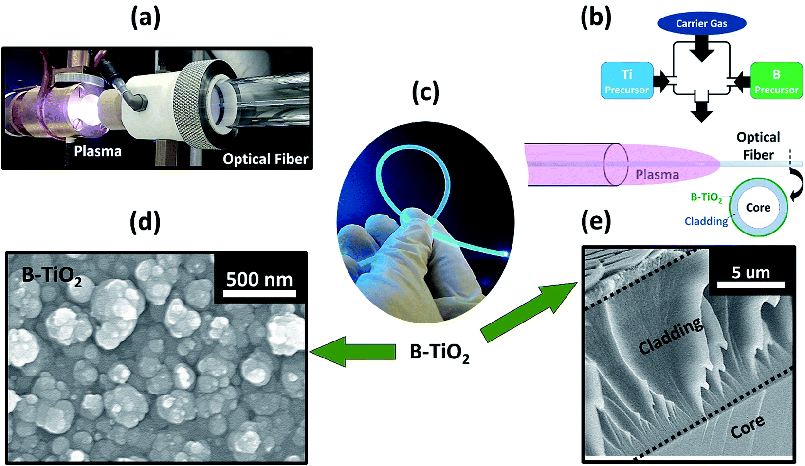 | ||
| Fig. 1 (a) Photo of the microwave plasma reactor and PMMA optical fibre being coated while passing through the plasma; (b) simplified scheme of the plasma coating process; (c) photo of the illuminated PMMA optical fibres coated with B-TiO2; (d) SEM top view and (e) SEM cross-sectional images of the B-TiO2 thin film deposited by AP-PECVD on the optical fibres. | ||
Cross-sectional SEM analysis showed the effective deposition of B-TiO2 thin films on OF substrates (Fig. 1d and e). It can be clearly observed that the thin films were well attached to the substrates, with a growth rate estimated around 72 nm min−1 (Fig. S1 and S2c†). In addition, top-down SEM analysis showed B-TiO2 thin films with spherical shaped particles (i.e. 50–150 nm in diameter) (Fig. 1d and e). As shown in Fig. 1d, there are some areas containing larger particles (i.e. 570 nm in diameter). We speculate that these particles are formed from the gas phase reaction of the precursors with the reactive species of the plasma discharge, inducing a high concentration of condensable species which further leads to high concentrations of nucleated particles that grow by condensation and coagulation.29 The numbers of formed particles in the gas phase and those observed at the surface of the films are therefore related to the precursor concentration, and also to the density and energy of the plasma post-discharge. It is worth mentioning that top-down view SEM images of both undoped and B-doped TiO2 samples were found to be very similar (Fig. S2†). Furthermore, the PMMA optical fiber has a melting point of 160 °C.30 The successful deposition on substrates of such chemical nature showed that the deposition temperature was at least below 160 °C.
To perform several important characterisations, the TiO2 and B-TiO2 thin films were also deposited on double-side polished silicon wafers (XRD & SIMS) and on microscope glass slides (UV-vis). The thin films, which exhibited a whitish and smooth appearance, were adherent to the substrates and homogenous over a length of 5 ± 1 mm in the direction parallel to the reactor's longitudinal axis. This area corresponds to the position where the PMMA optical fibres were placed during the coating experiments (Fig. 1). Raman spectroscopy and X-ray diffraction (XRD) were used to investigate the crystalline TiO2 phase of the undoped and B-doped TiO2 thin films (Fig. 2a and b). These studies confirmed the presence of solely the anatase TiO2 phase in both undoped and B-doped TiO2 thin films. The major scattering Eg band, typically found at 144 cm−1 in undoped anatase TiO2 materials,1,24 can be clearly observed at 145.8 cm−1 in Fig. 2a. This scattering Eg band was shifted to higher wavenumbers when TiO2 was B-doped (Fig. 2b), concretely to 155 cm−1, for B-TiO2 films. The described shifting has been observed previously when doping TiO2 with boron,31 due to the incorporation of boron into the TiO2 lattice, inducing a change in the mode of the vibration of pure TiO2. No signal due to boron or boron oxide (B2O3) was detected by Raman spectroscopy. Differences in the intensity can be observed as well. The intensity of the Raman spectra depends on (i) the intensity of the light source, (ii) the wavelength, indirectly proportional (1/λ4), (iii) the number of molecules/concentration of the sample and (iv) the scattering properties of the sample. The intensity of the peaks of the B-TiO2 was higher than in the case of the undoped sample (pure anatase). As the two first factors mentioned previously are similar, and the morphologies of the films by SEM are similar, the scattering properties of the sample might be similar, and the distribution and/or the concentration of the molecules (crystals) in B-TiO2 and undoped TiO2 are likely to be slightly different (see Fig. S3, ESI†).
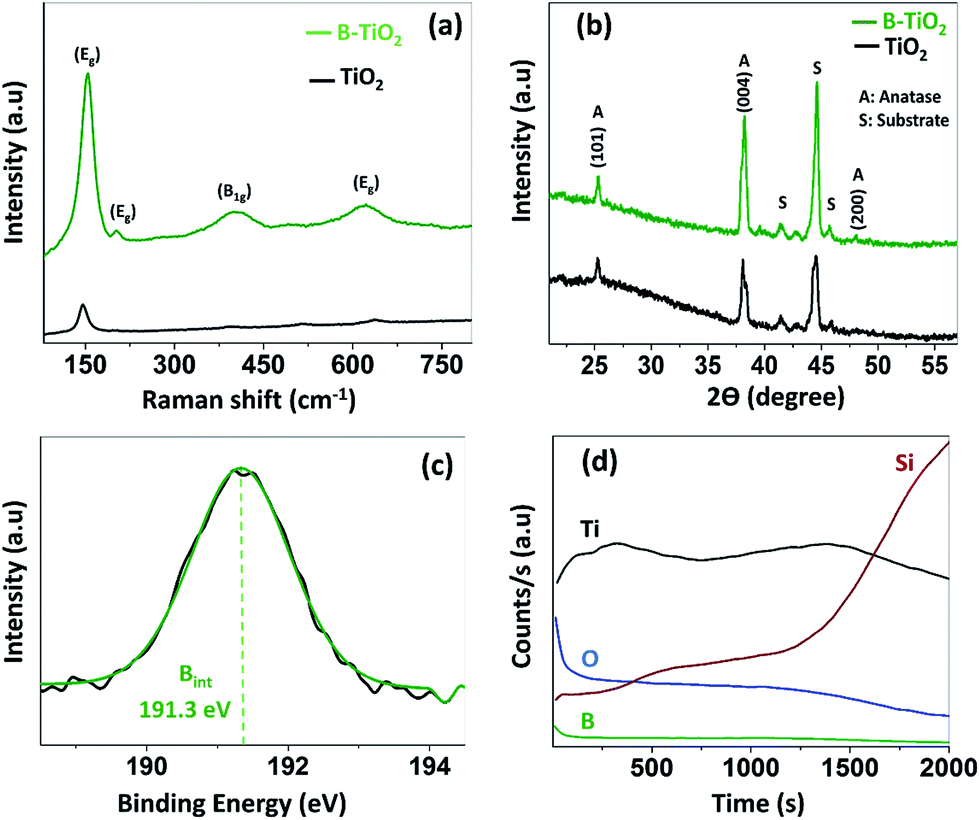 | ||
| Fig. 2 (a) Raman spectra of the anatase B-TiO2 thin film deposited on the polymeric optical fibre (POF). The Raman spectra of the undoped TiO2 thin film on the POF are shown for comparison; (b) XRD patterns of the B-TiO2 thin film deposited on planar silicon wafers; (c) XPS spectrum of the B 1s core level for the B-TiO2 thin film on the POF and (d) D-SIMS spectra of the B-TiO2 thin film on planar silicon wafers. | ||
In Fig. 2b, XRD analysis showed anatase TiO2 in both cases, undoped and doped B-TiO2. The planes (004) and (101) are shown as the preferred orientation for the growth of the TiO2 films, undoped and boron-doped, by AP-PECVD, under experimental conditions described in this work. It was not possible to give accurate cell parameters because of the preferred orientation. There was no noticeable shifting of the main peak for anatase TiO2, corresponding to the (101) plane. In both cases, for TiO2 and B-TiO2 the peak appeared around 25.3° (2 theta). To prove the presence of the dopant, X-ray photoelectron spectroscopy (XPS) and dynamic secondary ion mass spectrometry (D-SIMS) were used to study the nature and concentration of boron within the TiO2 coatings. As XPS is a surface-sensitive technique (≤10 nm),29 several depths within the bulk were investigated by etching the surface with argon sputtering. XPS analysis showed Ti 2p peaks at binding energies of 458.9 and 464.6 eV, which were attributed to the Ti–O bonds of Ti4+ in TiO2.32 No presence of reduced Ti3+ species was detected on the surface upon instrumental error (Fig. S2 in ESI†). The O 1s peak was observed at a binding energy value of 530.4 eV, confirming the formation of TiO2.32 All as-synthesised B-TiO2 films showed a single peak (Fig. 2c) at 191.3 eV, which was assigned to interstitial boron. Generally, when B is found at a binding energy between 191 and 192 eV then it is attributed to interstitial boron.12,26 Following this classification, the boron incorporated into the TiO2 deposited by AP-PECVD most likely occupies an interstitial position. The concentration of the different elements extracted from the XPS analysis showed that the percentages of Ti and oxygen remain similar in both cases, undoped and boron-doped TiO2 (Fig. S3†), except for carbon contamination, which appears much lower (ca. 3.5 at%) in the case of B-TiO2 thin films whereas in the undoped films it remains higher (ca. 8 at%). The total concentration of boron in the B-TiO2 thin film was found to be ca. 4 at%.
Further elemental studies were carried out using D-SIMS depth profile analysis (see Fig. 2c), confirming the presence of boron within the bulk of the film. Both analysis, XPS and D-SIMS, demonstrated that there is boron found as a dopant and that it is present on the surface and throughout the bulk of the boron-doped TiO2 thin film. We can confirm that the deposition is then anatase B-TiO2, most likely to be interstitial B-TiO2.
The photocatalytic activities of the undoped and B-doped TiO2 films were evaluated by the degradation of methylene blue (MB) in aqueous solution with an initial concentration of 10 µmol L−1. The samples with a size of 2.25 cm2 (i.e. 1.5 cm × 1.5 cm) were immersed in 2 mL of the dye solution in a 12 well plate (each sample in a different well). The well plate containing the samples and the dye was stirred using an orbital shaker (250 rpm) under irradiation with a 16 W black light lamp (Herolab; 365 nm, 2 mW cm−2). Fig. 3a shows the photocatalytic degradation of methylene blue under UV light (365 nm) for undoped TiO2 and B-TiO2 thin films deposited on silicon wafers by AP-PECVD. As shown in Fig. 3a, the degradation of MB is presented as the rate constant (k) of a pseudo kinetic first order reaction divided by the surface area of the samples. Given the equation ln(C0/C) = kt, where C0 and C are the initial concentration and the concentration at a certain point respectively, correlated with a certain time, t, and k is the rate constant of the reaction.33 The reaction was considered as the pseudo first order reaction as the graphic representation was almost linear (Fig. S4†).
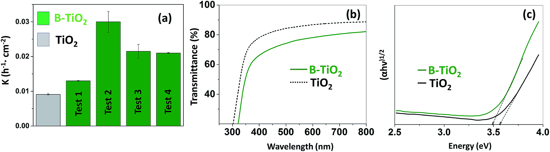 | ||
| Fig. 3 (a) Representation of the photodegradation of methylene blue for undoped TiO2 and B-TiO2 thin films as a function of rate constant of the reaction (h−1 cm−2). For the B-TiO2 thin film, different bars corresponding to different consecutive tests are presented. In the case of the undoped TiO2 thin film, the average of all the tests is presented; (b) transmittance spectra of undoped and B-TiO2 thin films on microscope glass slides; (c) Tauc plot for the calculation of the band gap for the undoped and B-TiO2 thin films on microscope glass slides. | ||
Typical synthetic methods, used to produce B-TiO2 photocatalytic materials, such as sol–gel and hydrothermal synthesis may produce materials with varying boron content and surface area, potentially affecting the performance of B-TiO2 photocatalysts.26 In contrast, the use of PECVD methods allows the synthesis of films with a homogeneous B content across the photocatalyst bulk, as well as comparable surface properties. Here, we observed that the incorporation of B into the TiO2 lattice was beneficial from a photocatalytic point of view. It is fundamental to mention that B can be added in two different oxidation states, interstitially (Bint) sitting in the lattice of TiO2 and substitutionally (Bsub) replacing O sites.12,24–26 When boron occupies an O-substitutional vacancy, the resulting B-TiO2 appears as a metastable species, which decomposes over time,13 whereas interstitial boron-doped TiO2 has been reported to be very stable over time for several photocatalytic cycles and even after the annealing process at relatively high temperature.28 The presence of both species (Bint + Bsub), within the TiO2 lattice, has been previously reported.13
When boron occupies simultaneously both positions within the TiO2 lattice, the absorbance of UV light and also the absorbance in the visible range of the spectra increase, even the Bsub disappears and decomposes under mild conditions. The higher photoactivity of TiO2–Bint under UV light, as compared to that of TiO2–Bint+sub, is mainly due to the delayed recombination processes even though the optical band gap is not significantly varied.25 In Fig. 3c, the graphic calculation of the optical band gap (Tauc method) for both undoped and boron-doped TiO2 thin films is presented. Both experimental values for the band gap are very close to each other, 3.56 eV for the undoped and 3.48 eV for the B-TiO2. The enhancement of absorbance in the UV region increases the number of photogenerated electrons and holes to participate in the photocatalytic reaction, which can enhance the photocatalytic activity of TiO2, whereas the band gap does not show anything more than a slight decrease in energy. The boron located at the interstitial site develops a shallow level, below the conduction band (CBM) due to the formation of a B–O–Ti bond. The shallow level seems to act as a trapping site for the photogenerated electrons to increase the lifetime and decrease the recombination process. This level hardly affects the band gap but plays a major role in trapping the photogenerated electrons.13,28
In Fig. 3a, it can be observed that both boron-doped and undoped TiO2 showed photoactivity under UV light (365 nm). When comparing the photocatalytic performance of B-TiO2 with that of undoped TiO2, after several cycles of photocatalysis for the same samples, a noticeable increase can be observed in the case of boron-doped anatase TiO2. There is a remarkable increase in the performance when comparing the first cycle of photocatalysis to the second one. The presence of carbon on the surface after the synthesis of the films cannot be denied, as shown by XPS analysis, and, as previous cleaning of the films before the first run of photocatalysis was not conducted, the increase of the performance of both undoped and boron-doped samples could be explained because of the self-cleaning process of the films, induced by the UV radiation in the aqueous medium, moreover, in between the cycles, the samples were washed with ethanol and distilled water, to make sure that no methylene blue was left on the thin-films. The enhancement of the photocatalytic activity of B-TiO2 under UV light has been described previously and attributed to a narrowing in the band gap and the reduction of recombination rates for photoexcited e−/h+.13,14,27,28 It is commonly acknowledged that the photocatalytic process in TiO2 proceeds through two different pathways: (i) the reaction of h+ with surface H2O producing hydroxyl radicals and/or (ii) the reaction of e− with O2 creating superoxide radicals. These highly reactive radicals are responsible for the degradation of nearby organic pollutants like p-NP and MB dye. This process is mainly affected by the surface area, light absorption capability, and charge separation and transfer of the photocatalyst.
Conclusions
In summary, we investigated and synthesized anatase and boron-doped anatase TiO2 thin films by AP-PECVD. The B-TiO2 thin films were deposited on polymer substrates, which are sensitive to temperature, such as polymer optical fibers (PMMA core based). The depositions were performed in one step, with no need of annealing or post-treatment to obtain the desired photoactive anatase phase of TiO2 at low temperature. The POFs did not melt or burn after the deposition. The films presented reasonable rates for photodegradation of methylene blue, as no second step of annealing was performed.34 When compared to the undoped TiO2 films, the B-TiO2 films presented higher rates of photodegradation of the dye. Nevertheless, the optical properties of the thin films, both undoped and boron-doped anatase TiO2 seemed to be similar, with no significant change. On the other hand, further research has to be done in terms of controlling the exact amount of dopant, which will be incorporated within the anatase lattice by changing some of the deposition parameters. To the best of our knowledge this is the first time that doped-TiO2 has been synthesized and doped simultaneously at atmospheric pressure by PECVD and that doped-anatase TiO2 films are deposited in one-step on a thermo-sensitive polymeric matrix such as PMMA optical fibres. In addition, the described approach could pave the way for the low-temperature synthesis and deposition of other functional crystalline transition-metal oxides, including transparent conductive oxides and thermochromic oxides, on a wide range of substrates such as textiles and polymers.Experimental section
AP-PECVD apparatus and deposition
The plasma, a surface wave discharge, was generated at atmospheric pressure inside a quartz tube of 5 and 7 mm inner and outer diameter, respectively (Fig. 4). Plasma was generated by applying a high-frequency electric field to a gas (argon by Air Liquide, 99.99%) flowing in a discharge tube by means of a wave launcher. The MW generator with a frequency of 2.45 GHz is operated in continuous mode with a power of 200 W. The wave launcher (Surfatron 80 by SAIREM) is powered via a coaxial cable and cooled by water. The discharge tube is cooled by compressed air and its end is at a distance of 3 cm from the launching gap. The flow of discharge gas, i.e. argon, is maintained at 10 standard litre per minute (slm) by a MKS mass flow controller.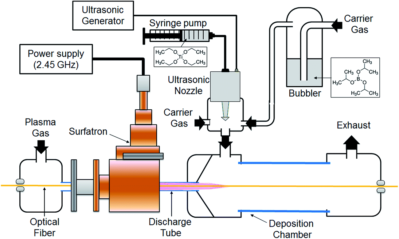 | ||
| Fig. 4 Schematic of the AP-PECVD apparatus set up for doping. | ||
Titanium ethoxide (Ti(OC2H5)4, 80%) was diluted in hexane (≥97%) to 0.5 M. In order to facilitate the injection of the precursor for the thin film deposition, the precursor flow rate was fixed at 10 µL min−1 and carried toward an ultrasonic nebulizing nozzle operating at 120 kHz (Sono-Tek). The drizzle formed at the outlet of the nozzle is composed of droplets with diameters ranging between 10 µm and 20 µm and which are carried by a mixture of gases, argon/oxygen, with a flow rate of 0.9 and 1 L min−1 respectively. The boron precursor, boron isopropoxide (B[(CH3)2CHO]3, ≥98%), was placed in a separate bubbler, connected to the nebulizing nozzle, joining simultaneously the flow of Ar (carrier gas). The solution was bubbled using a constant flow of 0.1 L min−1 of Ar, making the total flow of Ar carrier gas equal to 1 L min−1 (0.9 + 0.1 L min−1). The post-discharge distance from the launching gap was equal to 6 cm after the initiation of the plasma discharge, and the deposition was carried out for 10 minutes, keeping constant all the parameters previously described. Films were grown on both, side-glowing PMMA (2 mm of diameter; Luxylum) and the silica core with polyimide cladding (0.8 mm diameter; CeramOptec), optical fibers (OFs) and double side-polished silicon wafers (2 × 2 cm) were employed as substrates. For the OF substrates, pieces of 1 m length were placed from the left to the right side of the experimental setup and through the discharge tube in a horizontal position. In the present work, all the deposition experiments were performed in the static mode for a total duration of 2–3 min. The characterised area of the coated-OFs was located in the post-discharge region (from 5 to 8 cm from the launching gap) and close to the precursor injection outlet (i.e. 6 cm from the launching gap). Silicon wafer substrates were cleaned using absolute ethanol (97%) and dried with nitrogen prior to use. In the case of the silicon substrates, during the depositions, the substrate was placed in the deposition chamber in the same horizontal position as OF substrates (Fig. S4, ESI†), at a distance of 6 cm from the launching gap. The deposition time for the experiments carried out on Si wafers was 10 min.
Acknowledgements
M. Q.-G., K. B., N. D. B. and P. C. are grateful to the Luxembourgish “Fonds National de la Recherche” (FNR) for financial support through the PlasmOnWire CORE project (C13/MS/5894615). The authors of this work would like to thank and acknowledge the Department of Chemistry from the University College London (UCL) for the active collaboration and technical support provided. Dr Raúl Quesada-Cabrera and Dr Andreas Kafizas are thanked for useful discussions. Dr Robert Palgrave is also thanked for access and assistance with the XPS instrument.References
- A. Kafizas and I. P. Parkin, Chem. Soc. Rev., 2012, 41, 738–781 RSC.
- A. Kafizas, S. Kellici, J. A. Darr and I. P. Parkin, J. Photochem. Photobiol., A, 2009, 204, 183–190 CrossRef CAS.
- D. Grégori, I. Benchenaa, F. Chaput, S. Thérias, J.-L. Gardette, D. Léonard, C. Guillard and S. Parola, J. Mater. Chem. A, 2014, 2, 20096–20104 Search PubMed.
- K. Page, R. G. Palgrave, I. P. Parkin, M. Wilson, S. L. P. Savin and A. V. Chadwick, J. Mater. Chem., 2006, 17, 95–104 RSC.
- A. Mills, M. Crow, J. Wang, I. P. Parkin and N. Boscher, J. Phys. Chem. C, 2007, 111, 5520–5525 CAS.
- B. Liu and E. S. Aydil, J. Am. Chem. Soc., 2009, 131, 3985–3990 CrossRef CAS PubMed.
- A. Mills and S. Le Hunte, J. Photochem. Photobiol., A, 1997, 108, 1–35 CrossRef CAS.
- R. G. Palgrave and I. P. Parkin, J. Am. Chem. Soc., 2006, 128, 1587–1597 CrossRef CAS PubMed.
- R. Asahi, T. Mikawa, T. Ohwaki, K. Aoki and Y. Taga, Science, 2001, 293, 269–271 CrossRef CAS PubMed.
- R. Quesada-Cabrera, C. Sotelo-Vazquez, M. Quesada-Gonzalez, E. P. Melian, N. Chadwick and I. P. Parkin, J. Photochem. Photobiol., A, 2017, 333, 49–55 CrossRef CAS.
- T.-H. Xu, C.-L. Song, Y. Liu, G.-R. Han and J. Zhejiang, J. Zhejiang Univ., Sci., B, 2006, 7, 299–303 CrossRef CAS PubMed.
- K. Yang, Y. Dai and B. Huang, Phys. Rev. B: Condens. Matter Mater. Phys., 2007, 76, 1–6 Search PubMed.
- N. Patel, A. Dashora, R. Jaiswal, R. Fernandes, M. Yadav, D. C. Kothari, B. L. Ahuja and A. Miotello, J. Phys. Chem. C, 2015, 119, 18581–18590 CAS.
- E. Finazzi, C. Di Valentin and G. Pacchioni, J. Phys. Chem. C, 2009, 113, 220 CAS.
- J. Carlsson, Handb. Deposition Technol. Films Coat., 2010, 400–459 Search PubMed.
- D. Velten, V. Biehl, F. Aubertin, B. Valeske, W. Possart and J. Breme, J. Biomed. Mater. Res., 2002, 59, 18–28 CrossRef CAS PubMed.
- A. Zaleska, Recent Pat. Eng., 2008, 2, 157–164 CrossRef CAS.
- C. Burda, X. Chen, R. Narayanan and M. A. El-Sayed, Chem. Rev., 2005, 105, 1025–1102 CrossRef CAS PubMed.
- J. Guillot, E. Lecoq, D. Duday, E. Puhakka, M. Riihimäki, R. Keiski, J.-B. Chemin and P. Choquet, Appl. Surf. Sci., 2015, 333, 186–193 CrossRef CAS.
- K. Choy, Prog. Mater. Sci., 2003, 48, 57–170 CrossRef CAS.
- D. Mariotti, T. Belmonte, J. Benedikt, T. Velusamy, G. Jain and V. Svrcek, Plasma Processes Polym., 2016, 13, 70–90 CrossRef CAS.
- D. Li, A. Goullet, M. Carette, A. Granier, Y. Zhang and J. P. Landesman, Vacuum, 2016, 131, 231–239 CrossRef CAS.
- R. Maurau, N. D. Boscher, S. Olivier, S. Bulou, T. Belmonte, J. Dutroncy, T. Sindzingre and P. Choquet, Surf. Coat. Technol., 2013, 232, 159 CrossRef CAS.
- S. A. O'Neill, I. P. Parkin, R. J. H. Clark, A. Mills and N. Elliott, J. Mater. Chem., 2002, 13, 56–60 RSC.
- S. Dong, M. Watanabe and R. H. Dauskardt, Adv. Funct. Mater., 2014, 24, 3075–3081 CrossRef CAS.
- A. Zaleska, E. Grabowska, J. W. Sobczak, M. Gazda and J. Hupka, Appl. Catal., B, 2009, 89, 469–475 CrossRef CAS.
- P. Carmichael, D. Hazafy, D. S. Bhachu, A. Mills, J. A. Darr and I. P. Parkin, Phys. Chem. Chem. Phys., 2013, 15, 16788–16794 RSC.
- M. Quesada-Gonzalez, N. D. Boscher, C. J. Carmalt and I. P. Parkin, ACS Appl. Mater. Interfaces, 2016, 8, 25024–25029 CAS.
- N. D. Boscher, D. Duday, S. Verdier and P. Choquet, ACS Appl. Mater. Interfaces, 2013, 5, 1053 CAS.
- X. Zhu, E. G. Liu and E. Y. Guo, Microsyst. Technol., 2007, 13, 403–407 CrossRef CAS.
- W. Slink, J. Catal., 1981, 68, 423–432 CrossRef.
- S. J. Splinter, R. Rofagha, N. S. McIntyre and U. Erb, Surf. Interface Anal., 1996, 24, 181 CrossRef CAS.
- C. H. Wu and J. M. Chern, Ind. Eng. Chem. Res., 2006, 45, 6450 CrossRef CAS.
- X. J. Jin, J. Xu, X. F. Wang, Z. Xie, Z. Liu, B. Liang, D. Chen and G. Z. Shen, RSC Adv., 2014, 4, 12640–12648 RSC.
Footnote |
| † Electronic supplementary information (ESI) available: See DOI: 10.1039/c7ta02029e |
| This journal is © The Royal Society of Chemistry 2017 |