
 Open Access Article
 This Open Access Article is licensed under a
 Creative Commons Attribution 3.0 Unported Licence
Application of a hole transporting organic interlayer in graphene oxide/single walled carbon nanotube–silicon heterojunction solar cells†
LePing
Yu
,
Munkhbayar
Batmunkh
 ,
Tom
Grace
,
Mahnaz
Dadkhah
,
Cameron
Shearer
and
Joseph
Shapter
*
,
Tom
Grace
,
Mahnaz
Dadkhah
,
Cameron
Shearer
and
Joseph
Shapter
*
Centre for Nanoscale Science and Technology, School of Chemical and Physical Sciences, Flinders University, Bedford Park, South Australia 5042, Australia. E-mail: joe.shapter@flinders.edu.au
First published on 12th April 2017
Abstract
The solid-state hole transporting material 2,2′,7,7′-tetrakis(N,N′-di-p-methoxyphenylamine)-9,9′-spirobifluorene (spiro-OMeTAD) has been applied as an interlayer for graphene oxide/single walled carbon nanotube–silicon (GOCNT/Si) heterojunction solar cells, forming a GOCNT/spiro-OMeTAD/Si structure. An organic–aqueous transfer method was developed to deposit the GOCNT electrode onto the spiro-OMeTAD coated Si surface without dissolving the organic layer. The influence of the thickness of the organic layer and the thin film GOCNT transparent conducting electrodes as well as the doping of the films with gold chloride (AuCl3) on device performance is explored. With the optimized thickness of the spiro-OMeTAD interlayer and the GOCNT electrode with transmittance above 80% at 550 nm, devices with solar power conversion efficiency of 12.83 ± 0.22% have been fabricated. This study reveals that adding a hole-conducting organic interlayer is able to significantly minimize the recombination at the heterojunction interface. In addition to improving performance, the spiro-OMeTAD behaves as a physical protection layer to significantly enhance device stability.
1. Introduction
Thin film photovoltaics based on carbon materials, including carbon nanotubes (CNT)1–5 and graphene6–8 have attracted intense research interest for more than ten years due to the fantastic optoelectronic properties of these materials. Two-dimensional graphene oxide (GO), is an amphiphilic material which contains hydroxyl and carboxyl groups on the edges and epoxy and hydroxyl groups on the basal plane9,10 and has been used with CNTs in the fabrication of transparent conducting films.11 Due to its amphiphilic nature, GO can easily disperse agglomerated CNTs onto their surface and form a stable aqueous suspension.12 At the same time, GO sheets provide extra transport paths to some areas where the CNTs are disconnected.13,14 More attractively, the GOCNT hybrid films have the potential to be handled using aqueous solution based processes while pure CNT films have poor compatibility with water due to their highly hydrophobic nature.3GOCNT hybrid films have recently been applied with silicon to form heterojunction solar cells.15 In a typical graphene oxide/single walled carbon nanotube–silicon (GOCNT/Si) heterojunction, excitons are produced after light absorption by the silicon and they are then separated into free charge carriers under the influence of a built-in potential across the heterojunction at the interface (Fig. 1(a)). In the case of an n-type silicon/p-type GOCNT solar cell the resulting holes and electrons are collected within GOCNT film and Si, respectively.16–18 The exact nature of the heterojunction is still under debate, but the solar devices can be approximated as Schottky barrier, metal–insulator–semiconductor or p–n junctions.19 In most architectures, a thin SiO2 layer between CNT and Si improves diode properties by reducing the backward reaction arising from electron tunneling from Si to CNT.20
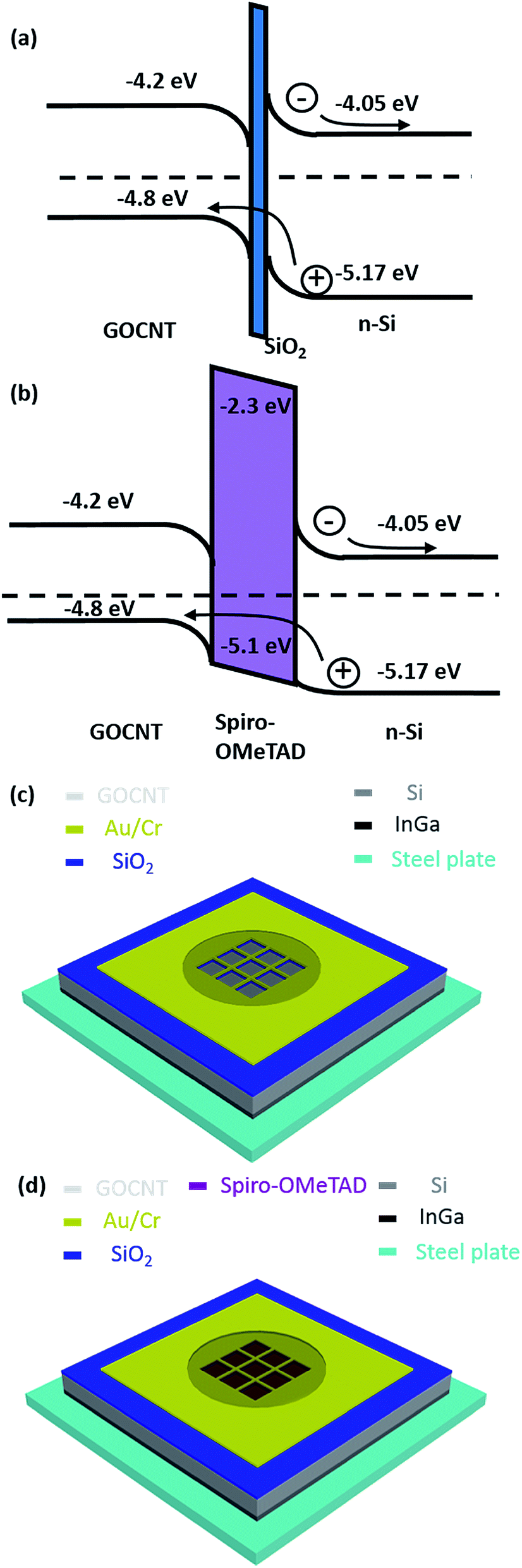 | ||
| Fig. 1 Schematic energy level alignment of GOCNT/Si heterojunction without (a) and with (b) a spiro-OMeTAD interlayer; schematic structures of (c) GOCNT/Si and (d) GOCNT/spiro-OMeTAD/Si solar cells. The band gap of GOCNT is taken from the S11 UV-Vis-NIR absorbance of the GOCNT film. | ||
Furthermore, there have been a few studies showing that the performance of CNT/Si device can be improved by adding an additional interlayer of conductive polymers, such as polyaniline, poly(3-hexylthiophene-2,5-diyl) (P3HT), and poly(3,4-ethylenedioxythiophene):poly(styrene sulfonate) (PEDOT:PSS),21,22 between the silicon surface and the CNT films. The major improvement observed after adding the interlayer is due to the conductive polymer acting as a hole transporting layer (HTL).23 In addition to these conductive polymers, 2,2′,7,7′-tetrakis(N,N′-di-p-methoxyphenylamine)-9,9′-spirobifluorene (spiro-OMeTAD) is the most commonly used HTL material in solid state dye sensitized and perovskite solar cells.24–26 Recently, Xu et al. reported that spiro-OMeTAD can also be applied as an interlayer in graphene/silicon solar cells to improve the hole transport as well to improve the diode properties of the heterojunction.16,23 On the basis of these excellent reports, spiro-OMeTAD may have the potential to be applied as efficient organic interlayers in GOCNT/Si devices to act as both a HTL27–29 and to improve the diode formed at the interface without absorbing a significant amount of solar irradiation (Fig. 1(b)).30–34
In this report, we explore the potential of employing spiro-OMeTAD as an interlayer between transparent conducting electrode of GOCNT and Si (GOCNT/spiro-OMeTAD/Si). Control devices without the HTL were fabricated, as shown in Fig. 1(c) and (d). Optimization of spiro-OMeTAD and GOCNT film thickness was achieved to maximize the device performance. The doping effect of gold chloride (AuCl3) was studied and the device stability behavior was analyzed over 2 weeks.
2. Experimental details
2.1. Preparation of material suspensions
The spiro-OMeTAD stock solution was prepared by dissolving 144.6 mg spiro-OMeTAD (Merck), 35 μL of a stock solution of 520 mg mL−1 lithium bis(trifluoromethylsulphonyl)imide (Li-TFSI) (Sigma-Aldrich) in acetonitrile, 57.6 μL 4-tert-butylpyridine (tBP) (Sigma-Aldrich) in 1 mL chlorobenzene.8The GO-CNT films were prepared by using GO to suspend SWCNTs in water. 3 mL of 5 mg mL−1 GO in ethanol (Graphene Supermarket, USA) was exposed to air in a 20 mL scintillation vial inside a fume hood at room temperature (20 °C) to obtain a solid. The GO solids were then dispersed in the deionized water by sonication for 30 min in an ice bath and the final concentration of the stock GO suspension was 1 mg mL−1. 5 mg CNT (P3-SWNT, Carbon Solutions Inc., USA) were dispersed with 50 mL of deionized water by sonication and the final concentration of the stock CNT suspension was 0.1 mg mL−1. In order to target the ideal mass ratio of GO![[thin space (1/6-em)]](https://www.rsc.org/images/entities/char_2009.gif) :CNT (1:2.25, according to our previous study, films with this ratio have the lowest sheet resistance), 2 mL GO stock suspension was added to 45 mL CNT stock suspension.15 The mixture suspension was dispersed by sonication in an ice bath for a further 90 min and centrifuged for 1 h at 17500g at 10 °C to remove any large agglomerates. The supernatant was collected and centrifuged in an identical manner. The second supernatant was collected and used as the source suspension for the preparation of GOCNT electrodes.
:CNT (1:2.25, according to our previous study, films with this ratio have the lowest sheet resistance), 2 mL GO stock suspension was added to 45 mL CNT stock suspension.15 The mixture suspension was dispersed by sonication in an ice bath for a further 90 min and centrifuged for 1 h at 17500g at 10 °C to remove any large agglomerates. The supernatant was collected and centrifuged in an identical manner. The second supernatant was collected and used as the source suspension for the preparation of GOCNT electrodes.
2.2. Preparation of solar devices
GOCNT electrodes were fabricated by vacuum filtration.35 In order to study the optoelectronic properties of GOCNT electrodes, different volumes of GOCNT stock suspension (200, 300, 400, 500, 600, 700, 800 μL) were diluted with deionized water to 250 mL. GO and CNT were collected on a mixed cellulose ester membrane (MCE, 0.45 μm, HAWP, Millipore, Australia). A nitrocellulose membrane (25 nm, VSWP, Millipore, Australia) with four holes (0.49 cm2 each) was placed beneath the MCE membrane. The different pore sizes of these two membranes leads to a faster flow rate at the areas of four holes and four identical GOCNT films were collected in one filtration on MCE. After being completely dried under gentle nitrogen flow, the individual GOCNT electrodes upon the MCE membranes were then cut with a pair of scissors and placed into an acetone bath for 3 × 30 min to dissolve the MCE, as shown in Fig. 2(a). A homemade Teflon spoon was used to transfer the now free-floating GOCNT films from the acetone bath to a water bath. The GOCNT electrodes were found to float on the surface of the water. They were then picked up with a prefabricated Si substrate to fabricate a solar cell device or a glass slide to determine the T as well as sheet resistance (RSheet) of the electrode.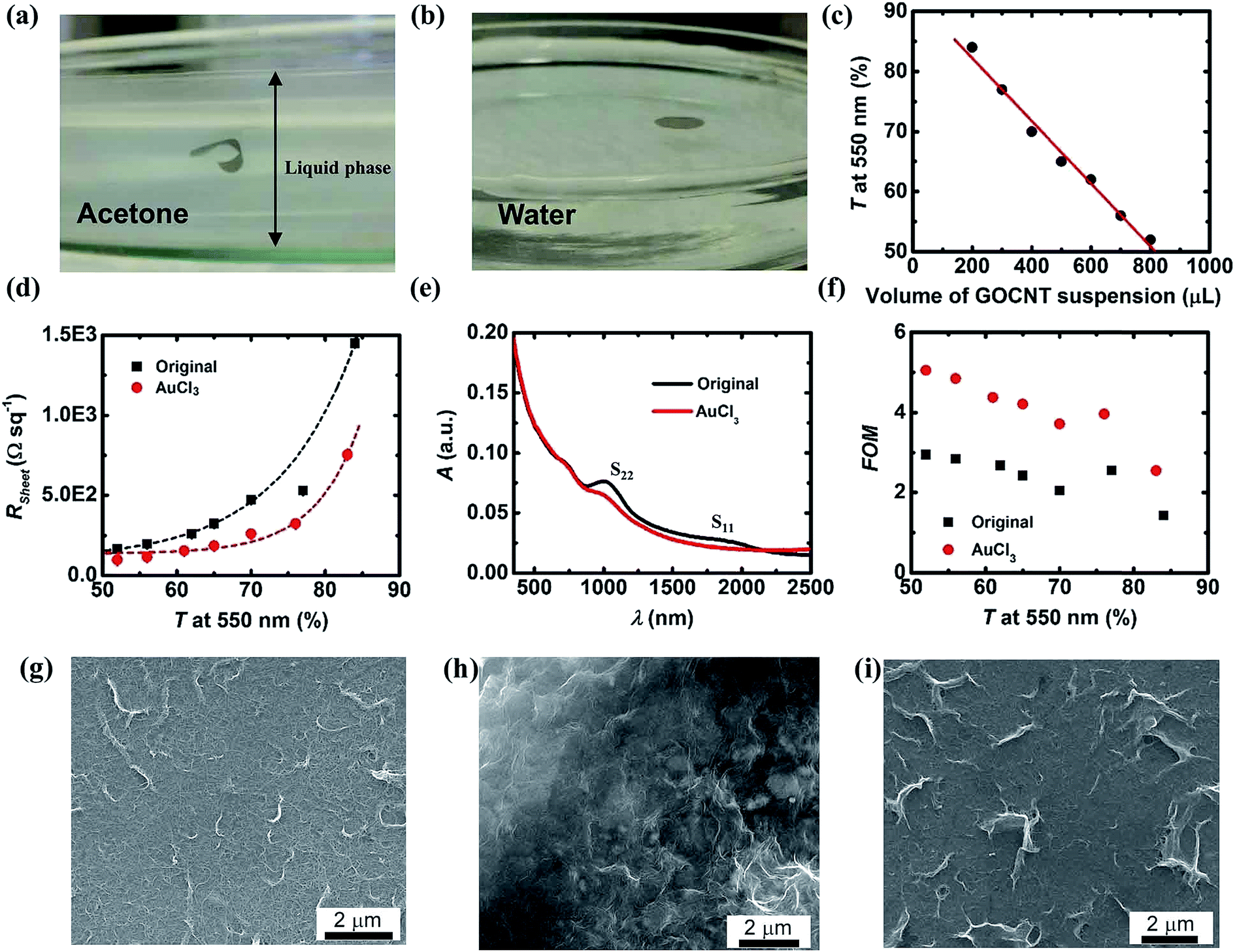 | ||
| Fig. 2 (a) GOCNT films (T = 77% at 550 nm) moving below the liquid surface in acetone and (b) standing above the surface of deionized water after dissolving MCE in a glass Petri dish, (c) T of GOCNT at 550 nm versus the volume of stock suspension used in vacuum filtration, (d) RSheet of GOCNT films with different T before and after AuCl3, (e) absorbance versus wavelength for the original and AuCl3 treated GOCNT films from 350 to 2500 nm, and (f) FOM of GOCNT films with different T before and after AuCl3. The solid line in (c), and short dashed curves in (d) are the linear and exponential fits for the data point. (g–i) SEM images of (g) pure CNTs, (h) pure GO and (i) GOCNT (1:2.25). | ||
Si solar devices were prepared from phosphorous doped silicon wafers (n-type, 5–10 Ω cm, 525 μm thick with a 100 nm thermal oxide, ABC GmbH, Germany). The gold grid structure was defined on the Si wafer by photolithography in a clean room (Class 1000). Positive photoresist (AZ1518, micro resist technology GmbH, Munich, Germany) was applied on the Si wafer by spin-coating (3000 rpm for 30 s), and then followed by soft baking (50 s at 100 °C) on a hot plate. After cooling the coated wafer to room temperature, the grid patterns were defined with a mask using a mask aligner (EVG 610, EVG). Then, the wafer was immersed in a developer solution (AZ 726 MIF, AZ electronic Materials, GmbH, Munich, Germany) for 15 s to develop the photoresist, rinsed with deionized water to remove the residue of the photoresist and dried under a nitrogen stream. The width of the grid lines is 0.01 mm and the spacing between each line is 0.5 mm. These grid lines are designed in a 3 × 3 mm square with the final active area of 0.087 cm2. 48 substrates were produced on a 4-inch wafer each time. The Si wafer with the defined pattern was post baked on a hot plate (50 s at 115 °C). The metal electrode (Au/Cr 90/5 nm, 95 nm in total) was deposited by a sputter coater (Quorumtech, Q300T-D) with a quartz crystal microbalance monitoring the thickness. Then, the substrate was immersed in acetone for 90 min followed by mild rubbing to dissolve and remove the photoresist. One drop of buffered oxide etch (6:1 of 40% NH4F and 49% hydrofluoric acid (HF), Sigma Aldrich, Australia) was applied to the active area with the defined Au grid for about 90 s to remove the top thermal silicon dioxide layer (SiO2). For GOCNT/Si devices, the Si substrate was then used to pick up the free-standing GOCNT on the surface of deionized water. For the GOCNT-spiro-OMeTAD/Si (and the spiro-OMeTAD/Si control) devices, different volumes of spiro-OMeTAD stock solution, 2.5, 10, 20, 30, 40, and 80 μL (30 μL for the spiro-OMeTAD/Si control device) were deposited onto the Si surface by spin-coating at 4000 rpm for 20 s in a nitrogen-filled glovebox. Then, these spiro-OMeTAD coated Si substrates were heated at 80 °C for 40 min in the glovebox and used to pick up the GOCNT films from deionized water. For GOCNT/Si and GOCNT/spiro-OMeTAD/Si devices, once the GOCNT films were dried by a very gentle nitrogen stream, the underside of the silicon was scratched with a diamond pen to create the conduction path from Si to the back electrode. The device was mounted onto a stainless steel plate with gallium indium eutectic (EGaIn), as shown in Fig. 1(c) and (d). For the spiro-OMeTAD/Si control devices, they were mounted on the stainless steel plates after the deposition of spiro-OMeTAD and scratching of the underside of the silicon. GOCNT was picked up in the same manner by microscope slide (instead of n-type Si) to determine the optical T and the RSheet. In order to explore the role of the spiro-OMeTAD interlayer in GOCNT/Si solar cells, 30 μL stock solution was used to apply the interlayer in spin-coating. During the optimization of GOCNT thickness in the GOCNT/spiro-OMeTAD/Si devices, 20 μL stock solution was used to apply the interlayer in spin-coating.
For the gold doping experiments, prior to solar cell testing, a post treatment was applied to the GOCNT films. 20 μL of 5 mM HAuCl4·3H2O (Sigma-Aldrich) aqueous solution was deposited on top of GOCNT by spin-coating at 5000 rpm for 20 s.
2.3. Solar cell testing
The performance of the solar cells was assessed by a custom LabviewTM virtual instrument connected with a Keithley 2400 source unit. The power density of the collimated xenon-arc light with an AM 1.5G filter at the device surface was calibrated to 100 mW cm−2 using a standard cell (PV Measurements, NIST-traceable certification). The devices were tested under both light and dark conditions to estimate the efficiency and the diode properties.Ideality and reverse saturation current (JSat) were extracted by fitting the dark J–V curve in to the following eqn (1) during the analysis of diode properties.
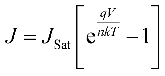 | (1) |
The Schottky barrier height (ϕB) related to JSat can be estimated by eqn (2) as follows:30
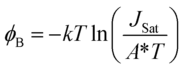 | (2) |
External quantum efficiency (EQE) of the devices was measured as a function of wavelength from 400 to 800 nm by passing the chopped light from a xenon source through a monochromator.
2.4. Characterization
The transparency of the SWCNT films at 550 nm was determined by UV Vis-NIR spectroscopy (Lambda 950 PerkinElmer) with the background subtraction of a clean glass slide. The RSheet of the GOCNT films was estimated by a four-point probe in linear configuration (Keithlink). The thickness of spiro-OMeTAD was measured by atomic force microscopy (AFM, Multimode, Bruker). Raman spectra of pure GO, CNT and GOCNT films are determined by AFM-Raman system (Nanonics-Horiba).3. Results and discussion
3.1. Device preparation and characterization
In this study, GOCNT films were prepared by vacuum filtration onto MCE and the films with MCE are immersed in acetone for 90 min to dissolve the MCE. The majority of the MCE quickly dissolves (<1 min) and the flexible GOCNT films freely move around in the liquid phase, as shown in Fig. 2(a). After being picked up and transferred from acetone to the deionized water by a homemade Teflon spoon, the GOCNT film stands on the water surface rigidly keeping its shape at the interface between the air and deionized water, as shown in Fig. 2(b).The transfer into water is very important in the fabrication of the solar cell devices because acetone quickly dissolves spiro-OMeTAD, but water does not. With floating GOCNT films on top of the water surface, spiro-OMeTAD coated Si substrates can pick up them without dissolving the spiro-OMeTAD. GO plays an essential role in the transfer process in the hybrid films. As a comparison, more than ten CNT films upon MCE were transferred in the same manner but they either disintegrated into pieces (most of them) or crumpled immediately upon contact with the water due to the highly hydrophobic nature of the CNT, as shown in Fig. S1(a) and (b).† By incorporating GO into the film structure, the mechanical properties as well as wettability of the hybrid improved due to the two dimensional feature and hydrophilic groups on GO.37,38 By pressing GOCNT film down into water with the spoon, it behaves in a similar way as it did in acetone, which is further evidence showing the improved compatibility with water, as shown in Fig. S1(c).† However, this transfer approach has its own limitation. When the T of the GOCNT film is above 80% (very thin films), the difficulty of the transfer increases significantly. Normally, the success rate of the transfer process for films with T of 77% is above 90% but this number is below 40% for films with T of 84% at 550 nm. In this study, films with T above 90% at 550 nm always broke during the transfer. Increasing the GO ratio in the hybrid film is expected to increase the transfer success rate of thin films but this sacrifices the optoelectronic properties significantly.15
Raman spectra of pure GO, CNT and GOCNT film on glass are shown in Fig. S2,† in which the ratio of D-band to G-band intensity (D/G ratio) is 1.10 for pure GO and 0.12 for pure CNT film and 0.21 for GOCNT film. The D band signal is caused by out-of-plane vibrations related to the defects on graphene structure while G band signal is a result of in-plane vibrations of sp2 bonded carbon atoms. Commonly, the functional groups on GO contribute to the D band intensity and higher D/G ratio indicates higher defect content. Both CNT and GO show typical values for low-functionalised CNTs and highly functionalised GO, respectively. The higher D/G ratio in the GOCNT film is a result of the mass ratio (2.25:1) of CNT to GO, not from the GO increasing the defect density of the CNTs.
As shown in Fig. 2(c), there is a linear correlation between the T of GOCNT films at 550 nm and the volume of the stock suspension used during vacuum filtration (as shown in eqn (S1)†). More GOCNTs are collected on the filter paper when higher volumes of stock suspension are used. As a result, thicker films are formed with more light being absorbed and the T at 550 nm decreases (complete UV-Vis spectrum presented in Fig. S2(b)†). As the T of GOCNT films decreases, more and more conducting paths are built. As a result, RSheet decreases with decreasing T, as shown in Fig. 2(d). In this study, AuCl3 is used as the dopant to improve the optoelectronic properties of GOCNT films by reducing the RSheet dramatically (Fig. 2(d)). Additionally, the RSheet has an exponential relationship with T for both original and AuCl3 doped films (eqn (S2) and (S3)†). As shown in Fig. 2(e) and S2(c),† the T of GOCNT film at 550 nm slightly decreases after doping with complete bleaching of S11 peak and suppressed S22 peak, which is the evidence of the shift of Fermi level into the van Hove singularities band of semiconducting SWCNT.39 The exact mechanism of the doping is controversial. Most researchers attribute the p-type doping to the reduction of cationic Au3+ to Au0 while others believe that the CNTs are more heavily doped by Cl with the formation of CNT-Cl where electrons of CNTs are further withdrawn to Cl.40
It is ideal that the window electrode of solar cells has both high T and low RSheet. Higher T indicates that more photons can reach and be absorbed by the Si substrate and lower RSheet infers that a more conducting network is built to transport the separated charge carriers. Thus, the final efficiency of the devices will be very sensitive to both the T and RSheet at the same time, but normally improving one of them sacrifices the other.5 Figure of merit (FOM) is widely used to easily compare the optoelectronic properties of transparent conducting electrodes with different T and RSheet. FOM is derived from eqn (3) and rearranged to eqn (4).
 | (3) |
 | (4) |
Normally, a higher value of FOM infers better optoelectronic properties. Fig. 2(f) shows the calculated FOM values for the GOCNT films correlated to T at 550 nm. As the AuCl3 can reduce the RSheet while maintaining the T at a relatively stable level, optoelectronic properties were improved after doping, which is also observed in the literature.40 For GOCNT films with high T, their FOM is lower than that of films with lower T. The FOM of the films ranges from 2 to 5, which is much lower than the value for a rigid transparent conducting glass, such as indium tin oxide coated glass (normally about 150).44 There are a number of explanations for the low recorded FOM values, such as the limited length of the CNTs (about 1 μm) and the low quantity of junctions in the thin films.5 But the FOM values are similar to the best CNT films used in CNT/Si heterojunction solar cells.45 Generally, FOM increases as the T decreases because of the dramatic reduction of RSheet with the decrease of T. Although CNT films with higher FOM (lower T) have better optoelectronic properties, that does not mean they are appropriate for the application of the window electrode for solar cells because high photocurrent output is always linked to high T. Therefore, in this study, a grid design of front metal electrode is applied across the entire active area to reduce the high internal series resistance of solar cells resulting from the relatively poor FOM of the films (details are shown in Experimental section).46
SEM images of pure CNT, pure GO and GOCNT (Fig. 2(g–i)) show that the produced film closely resembles that of pure CNT with only a few GO sheets observed. This finding is similar to the Raman and sheet resistance measurements in that the film properties much more closely match that of a pure CNT film than a GO film. This derives from the lower mass content of GO, and the role of GO to wrap around the CNT to facilitate dispersion in water and then support the film during aqueous transfer.
3.2. Initial photovoltaic device testing
The role of the GOCNT top electrode in the solar cells was explored by comparing the performance of two different types of devices including spiro-OMeTAD/Si and GOCNT/spiro-OMeTAD/Si before AuCl3 doping (in order to exclude the effect of the dopant). The J–V curves of these devices in light and dark conditions are shown in Fig. 3(a) and (b) with details shown in Table 1 and plotted in Fig. S3.† For these two types of devices, spiro-OMeTAD/Si has a much lower efficiency (0.05 ± 0.02%) due to the poor short circuit current density (JSC), open circuit voltage (VOC) and fill factor (FF). It also has the poorer diode properties with ideality, JSat and ϕB of 3.67 ± 0.49, 3.15 × 10⁻¹ ± 1.26 × 10⁻¹ mA cm−2, and 0.61 ± 0.07 eV, which indicates that the lower efficiency might be caused by severe recombination of the separated charge carriers related to the high RSheet of spiro-OMeTAD (above 106 Ω sq−1) and long carrier transport distance to the metal electrode. With the addition of GOCNT films (GOCNT/spiro-OMeTAD/Si), the efficiency (9.49 ± 0.29%, this value is close to the best SWCNT/Si device without any post treatment, 12.4%)47 has been significantly improved with JSC, VOC, FF increasing to 26.15 ± 0.26 mA cm−2, 0.550 ± 0.017 V, and 0.66 ± 0.02. This improvement can be attributed to the largely enhanced diode properties with ideality, JSat and ϕB of 1.19 ± 0.06, 1.99 × 10⁻⁶ ± 1.7 × 10⁻⁶ mA cm−2, and 0.91 ± 0.01 eV, which infers that the GOCNT films can reduce the recombination by collecting and transporting the separated charge carriers to the electrode swiftly due to a much lower RSheet (below 500 Ω sq−1). | ||
| Fig. 3 J–V curves of the spiro-OMeTAD/Si, GOCNT/Si and GOCNT/spiro-OMeTAD/Si devices under (a) light and (b) dark conditions before AuCl3 doping, (c) comparison between the dark curves of the GOCNT/Si device before and after AuCl3 doping and (d) EQE curves of the spiro-OMeTAD/Si after AuCl3 doping (the estimated JSC values from integration of the EQE curves for the spiro-OMeTAD/Si, GOCNT/Si and GOCNT/spiro-OMeTAD/Si are 1.49 mA cm−2, 24.74 mA cm−2 and 26.28 mA cm−2). Here, short dash curves are used to characterize the original device while the solid curves are used to characterize the device after AuCl3 doping. In the devices in this figure, the T of GOCNT films is 77% before AuCl3 and the thickness of spiro-OMeTAD layers is 90 nm. | ||
| Spiro-OMeTAD/Si | GOCNT/Si | GOCNT/spiro-OMeTAD/Si | ||||
|---|---|---|---|---|---|---|
| Original | AuCl3 | Original | AuCl3 | Original | AuCl3 | |
| Efficiency (%) | 0.05 ± 0.02 | 0.06 ± 0.02 | 6.80 ± 0.27 | 4.73 ± 0.33 | 9.49 ± 0.29 | 10.59 ± 0.27 |
| J SC (mA cm−2) | 1.32 ± 0.14 | 1.29 ± 0.16 | 23.02 ± 0.24 | 24.77 ± 0.13 | 26.15 ± 0.26 | 25.22 ± 0.18 |
| V OC (V) | 0.392 ± 0.002 | 0.392 ± 0.002 | 0.511 ± 0.006 | 0.424 ± 0.007 | 0.550 ± 0.017 | 0.576 ± 0.003 |
| FF | 0.10 ± 0.01 | 0.11 ± 0.01 | 0.58 ± 0.03 | 0.45 ± 0.03 | 0.66 ± 0.02 | 0.73 ± 0.01 |
| R Shunt (Ω) | 3.71 × 10³ ± 2.52 × 10³ | 6.41 × 10³ ± 3.42 × 10³ | 2.49 × 10⁵ ± 8.54 × 10⁴ | 6.52 × 10³ ± 1.54 × 10³ | 1.15 × 10⁴ ± 1.67 × 10⁴ | 8.22 × 10⁴ ± 9.67 × 10⁴ |
| R Series (Ω) | 6390 ± 258 | 6690 ± 176 | 72 ± 7 | 137 ± 12 | 63 ± 5 | 44 ± 3 |
| Ideality | 3.67 ± 0.49 | 3.78 ± 0.57 | 1.47 ± 0.07 | 2.55 ± 0.25 | 1.19 ± 0.06 | 1.12 ± 0.08 |
| J Sat (mA cm−2) | 3.15 × 10⁻¹ ± 1.26 × 10⁻¹ | 3.02 × 10⁻¹ ± 2.54 × 10⁻¹ | 6.51 × 10⁻⁵ ± 9.30 × 10⁻⁶ | 4.78 × 10⁻² ± 3.94 × 10⁻² | 1.99 × 10⁻⁶ ± 1.7 × 10⁻⁶ | 3.12 × 10⁻⁶ ± 0.7 × 10⁻⁶ |
| ϕ B (eV) | 0.61 ± 0.07 | 0.61 ± 0.08 | 0.82 ± 0.01 | 0.66 ± 0.05 | 0.91 ± 0.01 | 0.90 ± 0.01 |
By comparing the performance of GOCNT/Si and GOCNT/spiro-OMeTAD/Si devices before AuCl3 doping in order to exclude the influence of the dopant, the role of the spiro-OMeTAD interlayer is further studied. As shown in Fig. 3(a) and (b) and Table 1, the efficiency of the GOCNT/spiro-OMeTAD/Si device (9.49 ± 0.29%) is higher than that of GOCNT/Si counterpart (6.80 ± 0.27%). The improvement after adding the interlayer is observed due to the increase in FF from 0.58 ± 0.03 to 0.66 ± 0.02 and slight increases in JSC from 23.02 ± 0.24 to 26.15 ± 0.26 mA cm−2 and VOC from 0.511 ± 0.006 to 0.550 ± 0.017 V. With the interlayer, better diode properties, a lower ideality and JSat, are achieved. In addition, ϕB of the GOCNT/spiro-OMeTAD/Si device is about 0.1 eV higher than that of GOCNT/Si device and higher ϕB value normally indicates reduced recombination events, which is in line with the increase of FF as well as VOC. As mentioned earlier the GOCNT/Si interface does not represent an ideal Schottky junction and therefore the calculated ϕB values are derived from eqn (2) which assumes a much simpler interface. Nevertheless, previous reports of improvements in VOC and FF with the addition a conducting polymer interlayer into graphene–Si solar cell have also observed an increased ϕB upon interlayer incorporation.30 The increase in FF, VOC, JSat, and improvement in diode qualities indicate that the interlayer may acting as the HTL and electron blocking layer (EBL) at the same time.
3.3. AuCl3 doping
In order to improve the efficiency of the devices, AuCl3 doping was conducted to reduce the RSheet of GOCNT films, as discussed previously. The detailed influence of the AuCl3 doping on the solar cell performance are listed in Table 1 and plotted in Fig. S3.† For spiro-OMeTAD/Si devices, AuCl3 doping does not show any significant change to the performance, as shown in Table 1 and Fig. S3.† As shown in Fig. S4,† AuCl3 doping worsened the performance of GOCNT/Si device (to 4.73 ± 0.33%). The reduction in the performance might be caused by shorts induced by the Au nanoparticles bridging the front metal contact with Si surface.48 As the shorts cause a change in the diode properties of the heterojunction, as shown in Fig. 3(c) and Table 1, both the increased ideality and JSat reveal the increased recombination cases at the interface and the reduction in VOC and FF are in line with the increased recombination. Instead, when spiro-OMeTAD is applied as the interlayer in between GOCNT and Si, it improves the performance of GOCNT/spiro-OMeTAD/Si device (to 10.59 ± 0.27%, the value is close to the best SWCNT/Si devices after post treatment without antireflection layer, 13.7%).49 This improvement is due to the reduced RSheet of GOCNT films. Noticeably, in this case, the diode properties, including ideality and JSat, do not change much, as shown in Table 1, which suggests that the shorts do not take place because Au nanoparticles are physically blocked by the spiro-OMeTAD interlayer. Due to the improved performance, AuCl3 doping is used in all subsequent experiments and is signified by solid lines in J–V and EQE graphs.Fig. 3(d) shows the EQE curves for three types of devices after AuCl3. Spiro-OMeTAD/Si devices shows negligible photocurrent across the whole wavelength range from 300 to 1100 nm, which is consistent with the low JSC observed from the J–V curves. The GOCNT/Si device has a broad photocurrent contribution from 300 to 1000 nm while the EQE from 300 to 400 nm for GOCNT/spiro-OMeTAD/Si device is lower than that of GOCNT/Si devices. This feature is caused by the absorption of spiro-OMeTAD interlayer.50 There seems to be a bump at about 700 to 900 nm for GOCNT/spiro-OMeTAD/Si devices. Actually, this is mainly due to the absorption feature of Li-TFSI in the spiro-OMeTAD from 400 to 600 nm.51 The higher EQE values for GOCNT/spiro-OMeTAD/Si devices from 500 to 1000 nm is due to the suppressed charge recombination at the interface leading to higher overall PCEs.
3.4. Optimization of spiro-OMeTAD and GOCNT layer thickness
In order to optimize the thickness of the spiro-OMeTAD interlayer, different volumes (2.5, 10, 20, 30, 40 and 80 μL) of stock solution were applied on top of the Si surface. As shown in Fig. S5,† the thicknesses of these films determined by AFM are 10, 40, 60, 90, 120, and 240 nm respectively. Solar cells with different thicknesses of spiro-OMeTAD interlayer between the GOCNT and Si were fabricated and the details of their performance after AuCl3 doping are shown in Fig. 4 and S6.† | ||
| Fig. 4 The performance of GOCNT/spiro-OMeTAD/Si as a function of the thickness of spiro-OMeTAD interlayer applied on the Si surface after AuCl3 doping (a) J–V curves under light condition, (b) efficiency, (c) JSC, (d) EQE (the estimated JSC values of the devices with interlayer thickness of 10, 40, 60, 90, 120, 240 nm are 28.20 mA cm−2, 27.37 mA cm−2, 27.18 mA cm−2, 26.28 mA cm−2, 25.74 mA cm−2, and 24.40 mA cm−2), (e) VOC, (f) FF, (g) J–V curves under dark conditions, (h) ideality and (i) JSat. The devices in this figure are made using AuCl3 doped GOCNT films with T of 77% (T measured prior to doping) with spiro-OMeTAD layers of thicknesses ranging from 10 to 240 nm. | ||
The J–V curves of devices are shown in Fig. 4(a) and solar cells with an interlayer of 60 nm have the highest efficiency (11.41 ± 0.30%), as shown in Fig. 4(b). The change in efficiency with thickness follows a volcano like trend peaking at 60 nm. As the thickness of the interlayer increases from 10 to 240 nm, the JSC decreases from 26.84 ± 0.12 to 23.3 ± 0.19 mA cm−2 (Fig. 4(c)) because more light is absorbed by the interlayer with thickness resulting in less light absorption by the Si. The absorption of the spiro-OMeTAD interlayer and Li-TFSI around 500 nm is clearly increasing with thickness leading to lower EQE values at these wavelengths, as shown in Fig. 4(d). The VOC follows a similar volcano trend to that of PCE, with a maximum at 60 nm (Fig. 4(e)). Similarly the FF of devices peak at 60 nm interlayer thickness with sharp decrease for both thinner and thicker films (Fig. 4(f)). This improvement in FF is because even though more light is absorbed by the interlayer with increasing thickness, a better heterojunction is formed and the recombination is suppressed with the increasing interlayer thickness (except when it is very thick, 240 nm). However, when an extremely thick film (240 nm) is applied, the hole transport ability from the Si to GOCNT electrode might be limited. The diode properties of devices are estimated from the J–V curves under dark condition, as shown in Fig. 4(g)–(i). Because of the relatively large error bars, it is difficult to observe a clear trend for all of these devices. However, devices with the interlayer thickness of 40, 60 and 90 nm can be regarded very similar and they are better than devices with interlayer thickness of 10, 120 and 240 nm. Thus, when the thickness of the film is 60 nm, the interlayer is thick enough to form a good heterojunction, physically protect the Si surface while still allowing a significant amount of light pass through and is thin enough to be able to effectively pass the charge carriers to the conducting electrode. As a result, such devices have the best performance.
As mentioned before, a higher FOM is achieved with lower T while high T is closely related to excellent photocurrent output and thus the efficiency. Therefore, in this work, with an optimized spiro-OMeTAD thickness of 60 nm, GOCNT films with different T (56%, 65% and 76% and 83%) were next used to fabricate GOCNT/spiro-OMeTAD/Si devices to explore the influence of the GOCNT T. The details of the performance are shown in Fig. 5 and S7.† As shown in Fig. 5(a) and (b), the efficiency of the GOCNT/spiro-OMeTAD/Si increases from 8.52 ± 0.56% to 12.83 ± 0.22% with the increase of GOCNT T. As T of GOCNT increases, there is a significant increase in JSC from 19.97 ± 0.16 mA cm−2 to 28.1 ± 0.21 mA cm−2 while the VOC and FF are stabilized at about 0.575 V and 0.75, as shown in Fig. S7(a)–(d).† In terms of the diode properties, as shown in Fig. 5(c) and S7(g)–(i),† all of the GOCNT/spiro-OMeTAD/Si with GOCNT films of various T are similar, with ideality, JSat and ϕB being stable around 1.2, 10−6 mA cm−2 and 0.92 eV.
 | ||
| Fig. 5 (a) Efficiency, J–V curves in (b) light and (c) dark conditions of the AuCl3 doped GOCNT/spiro-OMeTAD/Si devices with different GOCNT T. The thickness of the spiro-OMeTAD in these devices is kept at 60 nm. | ||
Combining all the data on this set of experiments with changing GOCNT T, the T of GOCNT films does not have a dramatic effect on the heterojunction properties (with constant FF and VOC) but significantly alters the number of photons passing through the GOCNT film and the resulting number of excitons produced at the heterojunction interface (resulting in a higher JSC). This result shows that the solar cell performance is best for thin GOCNT films and is in contrast to most other reported results which show an optimal T of 50–70%.15,52 This finding highlights the importance of creating a consistent heterojunction across the interface (which is difficult in thin, often sparse, CNT films) in these heterojunction solar cells. This is an ideal scenario in which the amount of (potentially) costly CNT is minimized. Unfortunately, in this study, the T of GOCNT films are limited by the transfer approach and films with T above 90% at 550 nm could not be used to make devices. However, we expect that devices with GOCNT films of about 90% T would exhibit even better performance following previous work increasing CNT film T in solar cells.46
3.5. Photovoltaic performance stability
Finally, we investigated the stability of the devices over 2 weeks, as shown in Fig. 6 and S8.† Normally, in CNT/Si heterojunction solar cells, device performance degrades within a few days due to both the formation of a thick (>2 nm) SiO2 layer at the interface which restricts charge transport and the removal of weakly adsorbed dopants on the CNTs which reduce film conductivity.53–55 To first determine the degradation from the formation of SiO2 only, we compare the change in PCE for GOCNT/Si devices to that of GOCNT/sprio-OMeTAD/Si (red circles and blue open triangles in Fig. 6(a)). Without the conformal spiro-OMeTAD coating the photovoltaic performance decreases rapidly by about 30% in 14 days compared to a decrease of only 10% with the coating. This shows that the organic film is hindering unwanted SiO2 growth at the interface.56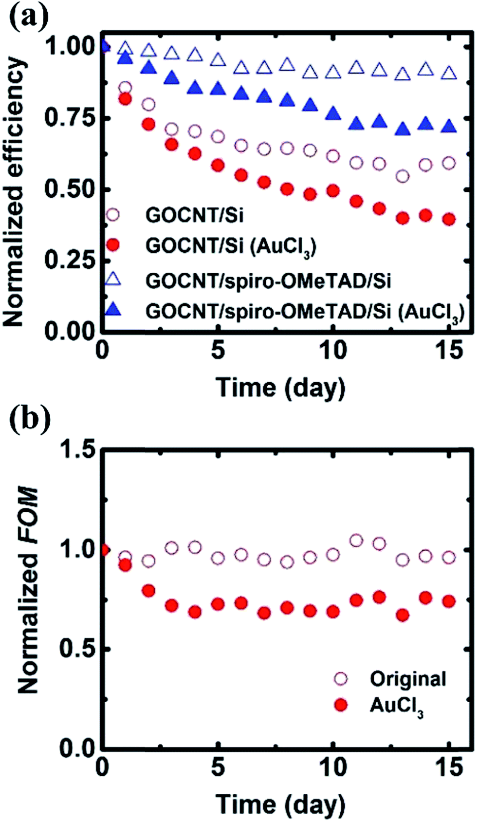 | ||
| Fig. 6 Degradation of the performance (a) efficiency of the devices and (b) FOM of the GOCNT films. The hollow and solid data points are used to characterize the properties of the devices or films with and without AuCl3 doping. | ||
To determine the stability of AuCl3 doping we compare the stability of GO/spiro-OMeTAD/Si with and without doping (both blue series in Fig. 6) in which it is clear that PCE drops more over two weeks when doping is employed. A similar degradation behavior was observed with AuCl3 doped few-layer graphene films in some previous studies.57–59 The small Au nanoparticles tend to aggregate due to the different surface energy between the graphitic structure and the Au nanoparticles. Furthermore, if some of the doping is being caused by bonded Cl−, these reactive groups are likely to react with air and be removed from the surface. The reduction in performance with doping closely resembles the reduction in film FOM (Fig. 6(b)) which indicates a strong correlation between CNT film conductivity and PCE. In addition to changes to the GOCNT film and Si interface, the conductivity of the organic interlayer degrades with time as the accumulation of Li-TFSI occurs, which is another factor responsible for the degradation.60 The GOCNT/spiro-OMeTAD/Si device without AuCl3 doping (hollow blue triangles) has the most stable normalized efficiency (above 0.9) after 15 days. This is comparable to the most stable CNT/Si heterojunction solar cells with the help of polymer encapsulating films.20
4. Conclusion
Spiro-OMeTAD has been added between GOCNT and Si layers to build GOCNT/spiro-OMeTAD/Si solar cells. AuCl3 was an effective dopant in improving the FOM of the GOCNT films. After the optimization of the thickness of organic layer and T of GOCNT top electrode, devices with 12.83 ± 0.22% efficiency have been fabricated. The spiro-OMeTAD interlayer plays several important roles in the devices. It can not only act as an HTL and EBL to improve the heterojunction properties by reducing charge recombination, but also serves as a protection layer which physically eliminates shorts caused by Au nanoparticles as well as the oxidation sources for the growth of SiO2.Acknowledgements
This work is supported by the South Australian node of both the Australian Microscopy and Microanalysis Research Facility (AMMRF) and the Australian National Fabrication Facility (ANFF).References
- T. A. Shastry and M. C. Hersam, Adv. Energy Mater., 2016, 1601205, DOI:10.1002/aenm.201601205.
- M. Batmunkh, M. J. Biggs and J. G. Shapter, Small, 2015, 11, 2963–2989 CrossRef CAS PubMed.
- S. Yadav, V. Kumar, S. Arora, S. Singh, D. Bhatnagar and I. Kaur, Thin Solid Films, 2015, 595, 193–199 CrossRef CAS.
- T. Grace, C. Shearer, D. Tune, L. Yu, M. Batmunkh, M. J. Biggs, Z. A. Alothman and J. G. Shapter, in Industrial Applications of Carbon Nanotubes, ed. Q. Li and T. Chen, Elsevier, Boston, 2017, pp. 201–249 Search PubMed.
- L. Yu, C. Shearer and J. Shapter, Chem. Rev., 2016, 116, 13413–13453 CrossRef CAS PubMed.
- K. P. Loh, S. W. Tong and J. S. Wu, J. Am. Chem. Soc., 2016, 138, 1095–1102 CrossRef CAS PubMed.
- X. Li, H. Zhu, K. Wang, A. Cao, J. Wei, C. Li, Y. Jia, Z. Li, X. Li and D. Wu, Adv. Mater., 2010, 22, 2743–2748 CrossRef CAS PubMed.
- M. Batmunkh, C. J. Shearer, M. J. Biggs and J. G. Shapter, J. Mater. Chem. A, 2016, 4, 2605–2616 CAS.
- L. Zhi-Jia, G. Hong-Zhang, Z. Xing, D. Baotan, D. Er-Xiong, W. Jing, L. Zhanguo, S. Baoquan, W. Jie and L. Juncheng, Nanotechnology, 2016, 27, 055601 CrossRef PubMed.
- J. Kim, L. J. Cote and J. Huang, Acc. Chem. Res., 2012, 45, 1356–1364 CrossRef CAS PubMed.
- S.-X. Da, J. Wang, H.-Z. Geng, S.-L. Jia, C.-X. Xu, L.-G. Li, P.-P. Shi and G. Li, Appl. Surf. Sci., 2017, 392, 1117–1125 CrossRef CAS.
- J.-Q. Huang, Z.-L. Xu, S. Abouali, M. Akbari Garakani and J.-K. Kim, Carbon, 2016, 99, 624–632 CrossRef CAS.
- J.-Y. Lin, A.-L. Su, C.-Y. Chang, K.-C. Hung and T.-W. Lin, ChemElectroChem, 2015, 2, 720–725 CrossRef CAS.
- T. Kim, J. Park, J. Sohn, D. Cho and S. Jeon, ACS Nano, 2016, 10, 4770–4778 CrossRef CAS PubMed.
- L. Yu, D. Tune, C. Shearer and J. Shapter, ChemSusChem, 2015, 8, 2940–2947 CrossRef CAS PubMed.
- D. D. Tune, B. S. Flavel, R. Krupke and J. G. Shapter, Adv. Energy Mater., 2012, 2, 1043–1055 CrossRef CAS.
- L. P. Yu, D. Tune, C. Shearer, T. Grace and J. Shapter, IEEE J. Photovolt., 2016, 6, 688–695 CrossRef.
- L. P. Yu, D. D. Tune, C. J. Shearer and J. G. Shapter, Sol. Energy, 2015, 118, 592–599 CrossRef CAS.
- F. De Nicola, M. Salvato, C. Cirillo, M. Crivellari, M. Boscardin, M. Passacantando, M. Nardone, F. De Matteis, N. Motta, M. De Crescenzi and P. Castrucci, Carbon, 2017, 114, 402–410 CrossRef CAS.
- Y. Jia, P. X. Li, X. C. Gui, J. Q. Wei, K. L. Wang, H. W. Zhu, D. H. Wu, L. H. Zhang, A. Y. Cao and Y. Xu, Appl. Phys. Lett., 2011, 98, 133115 CrossRef.
- L. Yu, D. D. Tune, C. J. Shearer and J. G. Shapter, ChemNanoMat, 2015, 1, 115–121 CrossRef CAS.
- D. D. Tune, B. S. Flavel, J. S. Quinton, A. V. Ellis and J. G. Shapter, ChemSusChem, 2013, 6, 320–327 CrossRef CAS PubMed.
- D. Xu, X. Yu, D. Gao, X. Mu, M. Zhong, S. Yuan, J. Xie, W. Ye, J. Huang and D. Yang, J. Mater. Chem. A, 2016, 4, 11284–11291 CAS.
- J. Lee, M. M. Menamparambath, J. Y. Hwang and S. Baik, ChemSusChem, 2015, 8, 2358–2362 CrossRef CAS PubMed.
- M. H. Li, C. W. Hsu, P. S. Shen, H. M. Cheng, Y. Chi, P. Chen and T. F. Guo, Chem. Commun., 2015, 51, 15518–15521 RSC.
- U. Bach, D. Lupo, P. Comte, J. E. Moser, F. Weissortel, J. Salbeck, H. Spreitzer and M. Gratzel, Nature, 1998, 395, 583–585 CrossRef CAS.
- Z. Yuan, Z. Wu, S. Bai, Z. Xia, W. Xu, T. Song, H. Wu, L. Xu, J. Si, Y. Jin and B. Sun, Adv. Energy Mater., 2015, 5, 1500038 CrossRef.
- A. Abrusci, S. D. Stranks, P. Docampo, H.-L. Yip, A. K. Y. Jen and H. J. Snaith, Nano Lett., 2013, 13, 3124–3128 CrossRef CAS PubMed.
- H.-W. Chen, T.-Y. Huang, T.-H. Chang, Y. Sanehira, C.-W. Kung, C.-W. Chu, M. Ikegami, T. Miyasaka and K.-C. Ho, Sci. Rep., 2016, 6, 34319 CrossRef CAS PubMed.
- H. He, X. Yu, Y. Wu, X. Mu, H. Zhu, S. Yuan and D. Yang, Nano Energy, 2015, 16, 91–98 CrossRef CAS.
- K. Ruan, K. Ding, Y. Wang, S. Diao, Z. Shao, X. Zhang and J. Jie, J. Mater. Chem. A, 2015, 3, 14370–14377 CAS.
- S. Wang, W. Yuan and Y. S. Meng, ACS Appl. Mater. Interfaces, 2015, 7, 24791–24798 CAS.
- K. Zhang, L. Wang, Y. Liang, S. Yang, J. Liang, F. Cheng and J. Chen, Synth. Met., 2012, 162, 490–496 CrossRef CAS.
- L. Yang, X. Yu, M. Xu, H. Chen and D. Yang, J. Mater. Chem. A, 2014, 2, 16877–16883 CAS.
- F. Wu, X. Li, Y. Tong and T. Zhang, J. Power Sources, 2017, 342, 704–708 CrossRef CAS.
- S. K. Cheung and N. W. Cheung, Appl. Phys. Lett., 1986, 49, 85–87 CrossRef CAS.
- Y. Y. Wang, G. Colas and T. Filleter, Carbon, 2016, 98, 291–299 CrossRef CAS.
- R. Rasuli, Z. Mokarian, R. Karimi, H. Shabanzadeh and Y. Abedini, Thin Solid Films, 2015, 589, 364–368 CrossRef CAS.
- J. N. Tey, X. Ho and J. Wei, Nanoscale Res. Lett., 2012, 7, 548 CrossRef PubMed.
- S. M. Kim, K. K. Kim, Y. W. Jo, M. H. Park, S. J. Chae, D. L. Duong, C. W. Yang, J. Kong and Y. H. Lee, ACS Nano, 2011, 5, 1236–1242 CrossRef CAS PubMed.
- S. De and J. N. Coleman, ACS Nano, 2010, 4, 2713–2720 CrossRef CAS PubMed.
- L. Hu, D. S. Hecht and G. Grüner, Nano Lett., 2004, 4, 2513–2517 CrossRef CAS.
- B. Ruzicka, L. Degiorgi, R. Gaal, L. Thien-Nga, R. Bacsa, J. P. Salvetat and L. Forro, Phys. Rev. B: Condens. Matter Mater. Phys., 2000, 61, R2468–R2471 CrossRef CAS.
- M. Duta, M. Anastasescu, J. M. Calderon-Moreno, L. Predoana, S. Preda, M. Nicolescu, H. Stroescu, V. Bratan, I. Dascalu, E. Aperathitis, M. Modreanu, M. Zaharescu and M. Gartner, J. Mater. Sci.: Mater. Electron., 2016, 27, 4913–4922 CrossRef CAS.
- J. Y. Li, Y. Zhu, X. Wang, N. Wang and J. Zhang, J. Appl. Phys., 2014, 116, 023101 CrossRef.
- L. Yu, T. Grace, M. D. Jazi, C. Shearer and J. Shapter, Solar RRL, 2017 DOI:10.1002/solr.201600026.
- F. Wang, D. Kozawa, Y. Miyauchi, K. Hiraoka, S. Mouri, Y. Ohno and K. Matsuda, ACS Photonics, 2014, 1, 360–364 CrossRef CAS.
- X. Li, Y. Jung, J.-S. Huang, T. Goh and A. D. Taylor, Adv. Energy Mater., 2014, 4, 1400186 CrossRef.
- J. M. Harris, M. R. Semler, S. May, J. A. Fagan and E. K. Hobbie, J. Phys. Chem. C, 2015, 119, 23293 CAS.
- J. H. Noh, N. J. Jeon, Y. C. Choi, M. K. Nazeeruddin, M. Gratzel and S. I. Seok, J. Mater. Chem. A, 2013, 1, 11842–11847 CAS.
- A. Abate, T. Leijtens, S. Pathak, J. Teuscher, R. Avolio, M. E. Errico, J. Kirkpatrik, J. M. Ball, P. Docampo, I. McPherson and H. J. Snaith, Phys. Chem. Chem. Phys., 2013, 15, 2572–2579 RSC.
- D. D. Tune and J. G. Shapter, Nanomaterials, 2013, 3, 655–673 CrossRef PubMed.
- K. Cui and S. Maruyama, IEEE Nanotechnol. Mag., 2016, 10, 34–41 CrossRef.
- S. L. Hellstrom, M. Vosgueritchian, R. M. Stoltenberg, I. Irfan, M. Hammock, Y. B. Wang, C. Jia, X. Guo, Y. Gao and Z. Bao, Nano Lett., 2012, 12, 3574–3580 CrossRef CAS PubMed.
- D. Hedman, H. Reza Barzegar, A. Rosén, T. Wågberg and J. Andreas Larsson, Sci. Rep., 2015, 5, 16850 CrossRef CAS PubMed.
- L. J. Larsen, C. J. Shearer, A. V. Ellis and J. G. Shapter, RSC Adv., 2015, 5, 38851–38858 RSC.
- M. Abdullah-Al-Galib, B. Hou, T. Shahriad, S. Zivanovic and A. D. Radadia, Appl. Surf. Sci., 2016, 366, 78–84 CrossRef CAS.
- K. Ki Kang, R. Alfonso, S. Yumeng, P. Hyesung, L. Lain-Jong, L. Young Hee and K. Jing, Nanotechnology, 2010, 21, 285205 CrossRef PubMed.
- F. Güneş, H.-J. Shin, C. Biswas, G. H. Han, E. S. Kim, S. J. Chae, J.-Y. Choi and Y. H. Lee, ACS Nano, 2010, 4, 4595–4600 CrossRef PubMed.
- Z. Hawash, L. K. Ono, S. R. Raga, M. V. Lee and Y. Qi, Chem. Mater., 2015, 27, 562–569 CrossRef CAS.
Footnote |
| † Electronic supplementary information (ESI) available. See DOI: 10.1039/c7ta01782k |
| This journal is © The Royal Society of Chemistry 2017 |