
 Open Access Article
 This Open Access Article is licensed under a
 Creative Commons Attribution 3.0 Unported Licence
Enhanced perovskite electronic properties via a modified lead(II) chloride Lewis acid–base adduct and their effect in high-efficiency perovskite solar cells†
Ngoc Duy
Pham
a,
Vincent Tiing
Tiong
a,
Peng
Chen
b,
Lianzhou
Wang
b,
Gregory J.
Wilson
c,
John
Bell
a and
Hongxia
Wang
 *a
*a
aSchool of Chemistry, Physics and Mechanical Engineering, Science and Engineering Faculty, Queensland University of Technology, Brisbane, Australia. E-mail: hx.wang@qut.edu.au
bSchool of Chemical Engineering, Australian Institute for Bioengineering and Nanotechnology, The University of Queensland, St Lucia, Brisbane, 4072, Australia
cCSIRO Energy, Mayfield West, NSW 2304, Australia
First published on 8th February 2017
Abstract
Methylammonium lead triiodide (MAPbI3) perovskite solar cells have gained significant attention with an impressive certified power conversion efficiency of 22.1%. Suppression of recombination at the interface and grain boundaries is critical to achieve high performance perovskite solar cells (PSCs). Here, we report a simple method to improve the performance of PSCs by incorporating a lead chloride (PbCl2) material into the MAPbI3 perovskite precursor through a Lewis acid–base adduct. The optimal concentration of PbCl2 that helps increase the grain size of MAPbI3 with introduction of the ideal amount secondary phases (lead iodide and methylammonium lead tri-chloride) is 2.5% (molar ratio, relative to lead iodide). Examination by steady-state photoluminescence and time-resolved photoluminescence has shown that devices based on MAPbI3-2.5% of PbCl2 facilitated longer charge carrier lifetime and electron–hole collection efficiency which is ascribed to reduced defects and concurrent improved material crystallinity. Electrochemical impedance spectra (EIS) of the corresponding PSCs have revealed that, compared to the pristine MAPbI3 perovskite film, the 2.5% PbCl2-additive increased the recombination resistance of the PSCs by 2.4-fold. Meanwhile, measurement of the surface potential of the perovskite films has indicated that the PbCl2-additive modifies the electronic properties of the film, shifting the fermi-level of the MAPbI3 film by 90 meV, leading to a more favourable energetic band matching for charge transfer. As a result, the performance of PSCs is enhanced from an average efficiency of 16.5% to an average efficiency of 18.1% with maximum efficiency reaching 19% due to the significantly improved fill-factor (from 0.69 to 0.76), while the hysteresis effect is also suppressed with the PbCl2-additive.
Introduction
Perovskites based on organic–inorganic lead halides with a formula of APbX3 (A = methylammonium (MA), formamidinium (FA); X = I, Br, and Cl) have attracted significant research interest due to their excellent optoelectronic properties and low-cost fabrication process.1 Perovskite solar cells (PSCs) which originally adopted the structure of a traditional dye-sensitized solar cell using an iodide/triiodide based liquid electrolyte and MAPbI3 nanoparticles as a light absorber were reported by Kojima et al. in 2009.1 Following this seminal report, a significant increase in device performance has been achieved through use of solid state hole transport materials for example, 2,2′,7,7′-tetrakis-(N,N-di-4-methoxyphenylamino)-9,9′-spirobifluorene more commonly referred to in the literature as Spiro-OMeTAD. The power conversion efficiency (PCE) of solid-state PSCs has soared from 9.7% in 2012 to a validated PCE of 22.1% in early 2016.3,4 Recent reports have suggested that the presence of a small amount of secondary phases such as lead iodide (PbI2) and/or methylammonium lead tri-chloride (MAPbCl3) in final perovskite films leads to improved performance of devices.2–4 Furthermore, these studies have shown that un-reacted PbI2 is mainly located at the grain boundaries (GBs) of the MAPbI3 film potentially passivating GBs and reducing recombination in the perovskite film,2 while MAPbCl3 acts as a template for the crystallization of MAPbI3 perovskite.5The solar cell devices that use chloride-based (Cl-based) perovskite layers have demonstrated superior PCE compared to solar cells made with Cl-free, MAPbI3 counter-parts.6–9 Stranks et al. pointed out that the electron and hole diffusion length of perovskite films made from the Cl-based precursor can be enhanced from about 100 nm to over 1 μm,10 indicating a reduced recombination in the bulk perovskite layer or at interfaces between the perovskite layer and selective contacts. Lead chloride (PbCl2) has been used as a Cl-source for preparing Cl-based perovskite films.11,12 The use of lead chloride (PbCl2) as an alternative to PbI2 in the perovskite precursor was reported to improve the uniformity and surface coverage of MAPbI3, controlling its nucleation.9 Higher concentrations of PbCl2 in the perovskite precursor induced increased numbers of perovskite crystallites, thus leading to improved film morphology. Furthermore, Huang et al. added additional PbCl2 (3 at% extra) to form a non-stoichiometric perovskite precursor with PbCl2![[thin space (1/6-em)]](https://www.rsc.org/images/entities/char_2009.gif) :MAI = 1.03:3 (molar ratio) and found that the excess PbCl2 facilitated the solubility of MAI in the perovskite precursor.13 A PCE up to 16.1% was achieved with an average PCE of 13.82% based on PbCl2-assisted heterogeneous nucleation crystallization. Nevertheless, the effect of excess PbCl2 on the nucleation process of MAPbI3 is still unclear. For instance, if PbCl2 acts as a heterogeneous nucleation site, then the small increment in the content of PbCl2 in the original precursor solution (from 1 to 1.03 molar ratio with respect to 3 MAI) actually did not significantly increase the number of seeds (no more than 3% with respect to the original number of seeds) for crystal growth.
:MAI = 1.03:3 (molar ratio) and found that the excess PbCl2 facilitated the solubility of MAI in the perovskite precursor.13 A PCE up to 16.1% was achieved with an average PCE of 13.82% based on PbCl2-assisted heterogeneous nucleation crystallization. Nevertheless, the effect of excess PbCl2 on the nucleation process of MAPbI3 is still unclear. For instance, if PbCl2 acts as a heterogeneous nucleation site, then the small increment in the content of PbCl2 in the original precursor solution (from 1 to 1.03 molar ratio with respect to 3 MAI) actually did not significantly increase the number of seeds (no more than 3% with respect to the original number of seeds) for crystal growth.
Although the benefits of Cl on electronic and morphological properties of MAPbI3 films are excellent, the exact location and the amount of Cl as well as the formation of Cl-based products in the final perovskite films remain unclear. Colella et al. have suggested that Cl is preferentially located near the perovskite/TiO2 interface, which in turns induces band banding and improves charge collection efficiency of TiO2.6 Song et al. proposed that the perovskite film prepared from a mixture of PbCl2 and MAI consists of MAPbI3 and secondary phases, e.g., PbI2 and MAPbCl3.4 The amount of these secondary phases strongly influences the PCE of PSCs. For instance, above the “optimal amount” of secondary phases, solar cells showed lower photovoltage while below that optimized value solar cells show lower photocurrent and thus lower PCE.4 In mixed halide perovskite films prepared from stoichiometric MAI:PbCl2 (3:1, molar ratio), the amount of the secondary phases is often controlled by tuning annealing temperature and time (100 °C, 90 minutes) which is somehow unreliable due to the intrinsic thermal instability of MAPbI3 perovskite.14
It has been established that due to the dewetting or agglomeration process of the as-deposited perovskite films prepared from a simple one-step spin-coating method, upon annealing, pin-holes and voids are often observed in the perovskite film even with inclusion of PbCl2 in the precursor and careful solution preparation.12 Several methods have been developed to control the crystallization processes of perovskites including using functional additives.3,15–19 Among them, the method based on antisolvent-dripping which takes place by sudden inducement of super-saturation in the film is found to be very effective,3,15,16 resulting in the formation of a smooth perovskite film with full surface coverage. Recently, Ahn et al. reported a modified antisolvent-dripping method which can effectively retard the crystal growth process of the perovskite material by forming a Lewis acid–base (MAI-PbI2-dimethyl sulfoxide (DMSO)) adduct and make the MAPbI3 film with high quality and full surface coverage.16 To date, as reported, this is an effective approach to produce high performance MAPbI3 solar cells. However, current–voltage hysteresis is still observed in the reported MAPbI3 perovskite solar cell probably due to an inherent unbalanced electron–hole diffusion length (∼130 nm for electrons, ∼90 nm for holes).20 Here we introduce a PbCl2 additive in the Lewis acid–base adduct method to fabricate a hysteresis-less high PCE solar cell, which has not been previously reported. Since the impact of PbCl2 on improving the morphology of the perovskite film using the Lewis acid–base adduct method is marginal, this allows us to uncover the underlying reasons for the change of device performance by focusing on the modification of electronic properties of the perovskite material. We have found that this simple method successfully establishes effective secondary phases (PbI2 and MAPbCl3) in the perovskite material while minimizing the adverse effect of annealing. These secondary phases and the incorporation of chloride into the perovskite lattice enable high PCE solar cells with less hysteresis and an improved fill factor.
Experimental
Materials preparation
All materials were purchased from Sigma-Aldrich and used as received without further purification unless otherwise stated. MAPbI3 perovskite precursor solution was prepared in an argon-filled glovebox by dissolving 461 mg of PbI2, 159 mg of methylammonium iodide (MAI) (Dyesol), and 78 mg of dimethyl sulfoxide (DMSO) in 700 mg of dimethyl formamide (DMF) at room temperature, under rigorous stirring for one hour. Mixed halide perovskite MAPbI3–PbCl2 additive precursor solution was prepared by adding different amounts of PbCl2 (1%, 2.5%, 5%, 7.5%, and 10% (molar ratio with respect to PbI2)) to the prepared MAPbI3 perovskite precursor. The solution was then magnetically stirred for an additional hour. The prepared perovskite solution was filtered by using a syringe filter (pore size: 0.22 μm) prior to use for deposition of the film. A solution for the hole transporting material was prepared by addition of 72.3 mg of 2,2′,7,7′-tetrakis-(N,N-di-4-methoxyphenylamino)-9,9′-spirobifluorene (Spiro-MeOTAD) (Borun New Material), 28.8 μL of 4-tert-butylpyridine, and 17.5 μL of bis(trifluoromethane)sulfonimide lithium (Li-TFSI) solution (520 mg of Li-TFSI in acetonitrile) into 1 mL of chlorobenzene.Device fabrication
Solar cells were fabricated using fluorine-doped tin oxide (FTO) coated glass (Nippon Electric Glass, 15 Ω □−1) as the substrate which was firstly patterned through partial removal of FTO via etching using 35.5 wt% HCl and zinc powder. The substrates were then cleaned in sequence in 5% Decon-90 detergent, and a mixture of acetone, isopropanol and ethanol for 20 min each in an ultrasonic bath. Prior to use, the substrates were treated with ultraviolet ozone for 30 min to fully remove organic solvent residuals. An electron transporting layer based on the TiO2 film (∼40 nm) was deposited in air via spin-coating a 0.15 M solution of titanium diisopropoxide bis(acetylacetonate) in 1-butanol at 2000 rpm for 20 s. The film was then dried at 125 °C for 5 min and annealed at 450 °C for 30 min. A mesoporous TiO2 (mp-TiO2) layer (∼200 nm) was spin-coated onto the compact TiO2 film using a diluted TiO2 paste (0.12 g TiO2 paste (Dyesol) in 1 mL of absolute ethanol) at 2000 rpm for 20 s, followed by sintering at 450 °C for 30 min. After cooling to room temperature, the film was treated with 20 mM TiCl4 aqueous solution at 90 °C for 10 min. The TiCl4-treated film was cleaned with distilled water and annealed again at 450 °C for 30 min. After this, the TiO2 coated film was treated in a UV-zone for 20 min before being transferred to an Ar-filled glovebox. Perovskite layers (∼400 nm) with and without PbCl2 in the perovskite precursor solution were deposited onto the prepared TiO2 layer at 4000 rpm for 20 s. During spin-coating, 0.5 mL of diethyl ether was dropped on the center of the spinning substrate before it turned turbid. The perovskite layer was then dried at 65 °C for 1 min, and annealed at 100 °C for 2 min.16 The hole-transport layer (∼200 nm) was deposited from the prepared Spiro-OMeTAD solution onto the as-prepared perovskite layer at 4000 rpm for 25 s. The device fabrication was finished by deposition of a 100 nm layer of gold film for back contact on the prepared sample via an e-beam evaporation process under 10−6 torr pressure.Characterization
The top-view and cross-sectional scanning electron microscopy (SEM) images of the samples were taken using a field emission scanning electron microscope (FSEM JOEL 7001F) at an acceleration voltage of 5 kV. The UV-vis absorbance spectrum was measured with a UV-visible spectrometer (Cary 50). The crystal structure of the perovskite film as-deposited on FTO/compact TiO2/mp-TiO2 was determined by X-ray diffraction (Rigaku SmartLab) with monochromatic CuKα (λ = 0.154 nm) as an excitation source. A scan rate of 1.5° per minute and a step size of 0.015° were used in the XRD measurement. The performance of perovskite devices was measured under irradiation of 100 mW cm−2 (AM1.5) provided by a solar simulator (Oriel Sol3A, Newport) equipped with a 450 W Xenon lamp. IPCE measurement was conducted by using a quantum efficiency system (IQE 200B, Newport) in AC mode. Electrochemical impedance spectroscopy (EIS) of the PSCs was performed in a frequency range from 1 MHz to 100 mHz using an electrochemical workstation (VSP BioLogic Science Instruments) at a forward bias of 0.5 V in darkness. An AC voltage with a perturbation amplitude of 10 mV was applied in the EIS measurement. X-ray photoelectron spectroscopy (XPS) (Kratos Axis Ultra) using mono Al Kα (1486.6 eV) X-rays was used to detect the elements in the perovskite film. For XPS depth profiling, a 4 keV Ar+ ion was used for the charge-up effect. The photoluminescence (PL) spectrum was measured with a fluorescence spectrometer (Edinburgh Instruments Ltd) at room temperature. The film was photo-excited by using a laser (474 nm) with a pulse wavelength of 82.4 ps. Scanning Kelvin Probe Force Microscopy (KPFM) (Oxford instrument, Asylum Research) was performed on the prepared perovskite film under ambient conditions using a NSG-03 Pt coated cantilever at room temperature. The work function of the cantilever was measured using a HOPG standard sample. The chloride analysis was performed on a Dionex RFIC ICS-2100 Ion Chromatography (IC) system (Thermo Scientific) with an ASDV auto sampler system. A Dionex-IonPac AS18 4 mm and a Dionex EGC-KOH II Cartridge were used as the column and eluent, respectively. The suppressor (ASRS 300, 4 mm) operated at 82 mA. The calibration standards were diluted from an IC standard (containing 1000 μg mL−1 of Cl) purchased from Choice Analytical. Perovskite/FTO samples (2 × 1.5 cm) were immersed into 2 mL of Milli-Q water in a clean beaker until the perovskite layer was fully removed. The amount of dissolved perovskite material in water was used for further calculation. 1.2 mL of the resulting solution was pipetted out and further diluted five fold for IC measurements.Results and discussion
Depicted in Fig. 1(a)–(e) are the top-view SEM images of perovskite layers with various concentrations of PbCl2 in the precursor solution (from 0% to 10% with respect to the content of PbI2). The MAPbI3 film consists of grains with the size of 100–300 nm which are connected closely, resulting in a pinhole-free and highly compact film (Fig. 1a), which is desirable for PSCs. When only 1% PbCl2 was added into the perovskite precursor, there is no observable change in the film morphology in terms of grain size and film compactness (Fig. 1b) compared to the pure MAPbI3 film. This indicates that a negligible amount of PbCl2 in the perovskite precursor does not dramatically change the surface morphology of the perovskite film in our experiments. This phenomenon is different from what has been reported previously where a small amount of PbCl2 (∼1%) significantly improved surface coverage of the perovskite film.13 It is ascribed to the effectiveness of the Lewis acid–base adduct method which results in high quality MAPbI3 perovskite films.16,21 However, when the PbCl2-additive increased to 2.5%, larger grains with the crystallite size in the range of 300–500 nm are observed in the perovskite film (Fig. 1c). This effect could be attributed to a better crystallization of the perovskite layer, which leads to larger perovskite crystals in the presence of PbCl2. Probably MAPbCl3 is formed first and then acts as a template to aid grain growth.5 To gain more insight into the influence of PbCl2 on the morphological properties of the perovskite film, the concentration of PbCl2 in the MAPbI3 precursor was further increased to 5%, 7.5%, and 10%, respectively. As shown in Fig. 1(d)–(f) under the same deposition and annealing conditions, there is no further increase in grain sizes of the perovskite material. Nevertheless, small voids/pinholes can be seen clearly at the GBs on the surface of perovskite films with precursor solutions in excess of 5% PbCl2. The number of voids/pinholes increases with the increase of PbCl2 concentration. It is known that voids at the GBs can increase recombination in the device due to poor contact/necking between the light absorbing particles, thus impacting device performance. Formation of voids in films with over 5% PbCl2 in the perovskite precursor might be a consequence of the different nucleation rates and competitive growth of nuclei MAPbI3, MAPbCl3 and PbI2, which somehow affects the surface coverage of the film.9 Furthermore, irregular grain sizes are also observed in the perovskite film with 10% PbCl2 in the precursor solution (Fig. 1f), which could be due to the coexistence of MAPbI3 and methylammonium lead chloride (MAPbCl3) as confirmed by XRD (see below). The above SEM results indicate that 2.5% PbCl2 provides the optimal quality of surface morphology of the perovskite film. | ||
| Fig. 1 Top-view SEM images of perovskite films. (a) MAPbI3, (b) MAPbI3 + 1% PbCl2, (c) MAPbI3 + 2.5% PbCl2, (d) MAPbI3 + 5% PbCl2, (e) MAPbI3 + 7.5% PbCl2, and (f) MAPbI3 + 10% PbCl2. | ||
Since the optimal light absorption and energy bandgap are very critical for the performance of a solar cell, the light absorption properties of the MAPbI3 film made from different contents of PbCl2 in the precursor were investigated by ultraviolet-visible (UV-vis) spectroscopy (Fig. S1†). However, negligible change is found in the onset light absorbing wavelength and the intensity of light absorption of the perovskite layers with the content of PbCl2 below 5%. A slight blue-shift in the UV-vis spectrum is observed with the film made from a higher content of the PbCl2 additive (above 5%), which could be related to incorporation of chloride into the MAPbI3 crystal lattice, which reduces the lattice symmetry and thus increases the material bandgap22 and the coexistence of a small amount of MAPbCl3. The reduction in intensity of light absorption of the film with a higher content of PbCl2 is associated with the existence of more voids as observed in Fig. 1(d)–(f) and possible secondary impurities such as PbI2 and MAPbCl3 in the film as indicated in the XRD (below).
To gain insight into the effects of the PbCl2-additive on the crystal structure of the perovskite material, X-ray diffraction (XRD) data were collected for the diffraction patterns of the films (Fig. 2). From the data, it is found that when the concentration of PbCl2 is less than 5%, all XRD peaks can be well indexed to the reflection of MAPbI3 without any impurities detected within the instrumental limit of the XRD facility. However, a small peak at 12.8° which is ascribed to the (001) plane of PbI2 is observed when the amount of PbCl2-additive exceeds 5%. For the film with 10% PbCl2, a diffraction peak at 15.6° which belongs to the reflection of the (110) plane of methylammonium lead tri-chloride (MAPbCl3) is also observed. It is worth noting that no peak from PbCl2 is observed in all the XRD spectra, indicating that the added PbCl2 is completely consumed in the reaction with MAI to either form PbI2 or MAPbCl3. This is in good agreement with a previous study.16 A moderate excess of PbI2 in the MAPbI3 perovskite film which mainly exists at GBs is beneficial because it forms an energy barrier that hinders leakage of both electrons and holes from MAPbI3 for recombination.23 However, a large amount of PbI2 in the perovskite film is detrimental for light harvesting due to its much larger bandgap (2.41 eV for PbI2) and low light absorption, which in turns reduces the current density of devices.2 Furthermore, a small shift of the XRD patterns towards the smaller angle of MAPbI3 was observed with the presence of PbCl2 in the precursor (Fig. 2(b)–(d)). For example, by comparison of the XRD patterns, it is found that peaks at 14.14° ((110) plane, Fig. 2b), 28.47° ((220) plane, Fig. 2c) and 31.9° ((310) plane, Fig. 2d) for the pristine MAPbI3 shift to 14.16° ((110) plane), 28.50° ((220) plane) and 31.93° ((310) plane) for the MAPbI3-2.5% PbCl2 additive. The shifts is slightly larger than the XRD measurement step (0.015°), suggesting the effect of inclusion of Cl on the crystal lattice of MAPbI3. Furthermore, the trend illustrating that the more PbCl2 in the MAPbI3 precursor leads to the more shift of the XRD patterns towards the smaller angle of MAPbI3 is observed, confirming that a certain amount of Cl might be incorporated into the crystal lattice of MAPbI3.
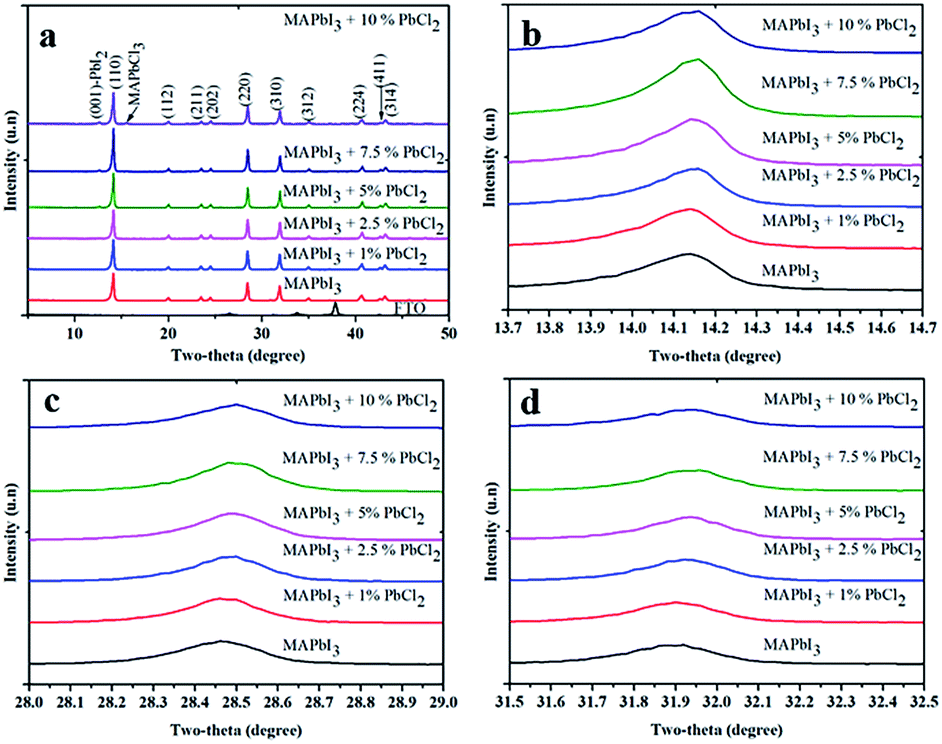 | ||
| Fig. 2 (a) XRD patterns of MAPbI3 films prepared from perovskite precursor solution with different concentrations of PbCl2. Zoom-in XRD patterns showing at (b) (110) lattice plane; (c) (220) plane; and (d) (310) plane. | ||
We have attempted to determine the chlorine content in the MAPbI3 films made from the PbCl2 additive based precursor by a conventional method such as X-ray photoelectron spectroscopy (XPS) (Fig. S2†). Nevertheless, no characteristic peak of chlorine was detected in the film even in the XPS depth profiling spectrum (Fig. S2†). The failure of XPS for detection of Cl in perovskite films could be due to the strong photon/ion energy, which destroys volatile Cl-based species. Unlike common techniques such as EDS and XPS, ion chromatography (IC) is a highly accurate non-destructive testing method, which guarantees that the measurement does not lose Cl-based species. The chloride content in the final perovskite films prepared from different concentrations of PbCl2 in the perovskite precursor solutions was assessed by IC as demonstrated in Table 1. It reveals that Cl remains in perovskite films after a mild annealing (2 min, 100 °C) which is consistent with previous reports.5,24 The preservation of Cl in our annealed perovskite films could be due to the high compactness of the as-deposited perovskite film which slows down the rates of diffusion of Cl to the surface and prevent its loss afterwards.25 The exact forms of Cl-based products are beyond the scope of this study; we speculate that the remaining chloride could incorporate into the MAPbI3 lattice, at the GBs, interfaces, or in MAPbCl3 form. The induced MAPbCl3 is not detected in the XRD pattern in low concentration PbCl2-based perovskite films (below 10%), which is presumably because of the poor crystallinity of the MAPbCl3-like form.5,26 Furthermore the unreacted PbI2 passivates GBs which generally worked as recombination centers.2
| Content of PbCl2 in the perovskite precursor (%, molar ratio relative to MAPbI3) | Content of Cl− ions in the perovskite precursor (%, molar ratio relative to MAPbI3) | Content of Cl− ions in the final perovskite films (%, molar ratio relative to MAPbI3) |
|---|---|---|
| 2.5 ± 0.2 | 5 ± 0.4 | 4.9 ± 0.2 |
| 5 ± 0.2 | 10 ± 0.4 | 10.1 ± 0.2 |
| 10 ± 0.2 | 20 ± 0.4 | 20.6 ± 0.2 |
To explore the benefits of the PbCl2-additive in the perovskite precursor on the performance of solar cells, solar cells based on different PbCl2 contents were fabricated and the comparison of Jsc, Voc, FF and PCE is summarized in Fig. 3(a)–(d). It is found that the PbCl2-additive does not significantly change the Voc and Jsc of the solar cells with the content of the PbCl2-additive up to 2.5%. Beyond this, Jsc decreases marginally which is ascribed to reduced light absorption associated with formation of PbI2 impurity and increased voids/pinholes. The most remarkable change is observed with respect to the FF of the solar cells. When the PbCl2 content is increased from 0% to 2.5%, the FF is improved from 0.69 to 0.76 primarily as decreased series resistance (Rs) and increased shunt resistance (Rsh) (Table 2). The decrease in Rs is presumably attributed to the reduction of GBs as observed in Fig. 1(a)–(c), while the increase in Rsh corresponds to improved perovskite film quality and more efficient interfacial charge transfer between MAPbI3 and TiO2 film. The increase of PbCl2 concentration to 5% led to an increased Rs and reduced Rsh, which could be due to the occurrence of more pinhole/voids and impurities as discussed above. With further increasing the PbCl2 content to 7.5%, devices exhibited higher Rs, yet higher average Rsh. However, an extremely large variation was observed, which is possibly related to the non-uniformity of the film due to the distribution of pinhole/voids and a large amount of impurities (PbI2 and MAPbCl3) in the perovskite film. Thus the devices with the 2.5% PbCl2 additive result in the maximum FF, which is in line with PCEs obtained. As a result, the best performance devices were obtained with the 2.5% PbCl2-additive in the precursor solution with an average Jsc of ∼23.5 mA cm−2, Voc of ∼1.04 V and FF of ∼0.75, leading to an average efficiency of 18.1% (based on a batch of 10 cells), which is much higher than that of devices without the PbCl2-additive which shows an average PCE of 16.5% (Jsc of ∼23.5 mA cm−2, Voc of ∼1.02 V, and FF of ∼0.69). The best performance of the 2.5% PbCl2-additive based cell produced an efficiency of 19% with details shown in the following section.
 | ||
| Fig. 3 Statistical parameters of (a) Voc, (b) Jsc, (c) FF, and (d) PCEs measured under reverse scanning (Voc, to Jsc) for 10 cells using MAPbI3 with varied contents of PbCl2 in the precursor. | ||
| Content of PbCl2 (%) | R s (Ω cm−2) | R sh (kΩ cm−2) |
|---|---|---|
| 0% | 46.9 ± 5.4 | 6.8 ± 1.7 |
| 1% | 42.0 ± 6.3 | 9.4 ± 1.9 |
| 2.5% | 31.9 ± 2.9 | 10.8 ± 1.8 |
| 5% | 34.1 ± 3.8 | 8.2 ± 1.4 |
| 7.5% | 38.6 ± 12.6 | 14.9 ± 8.6 |
| 10% | 33.8 ± 6.6 | 8.1 ± 1.1 |
The detailed cross-sectional SEM structure of a representative solar cell made from the precursor containing the 2.5% PbCl2-additive in MAPbI3 solution is depicted in Fig. 4a. As depicted, the perovskite layer is homogeneous with large crystals which connect closely and seem to form a monolithic layer from the mesoporous bottom layer to top, suggesting a low density of GBs.
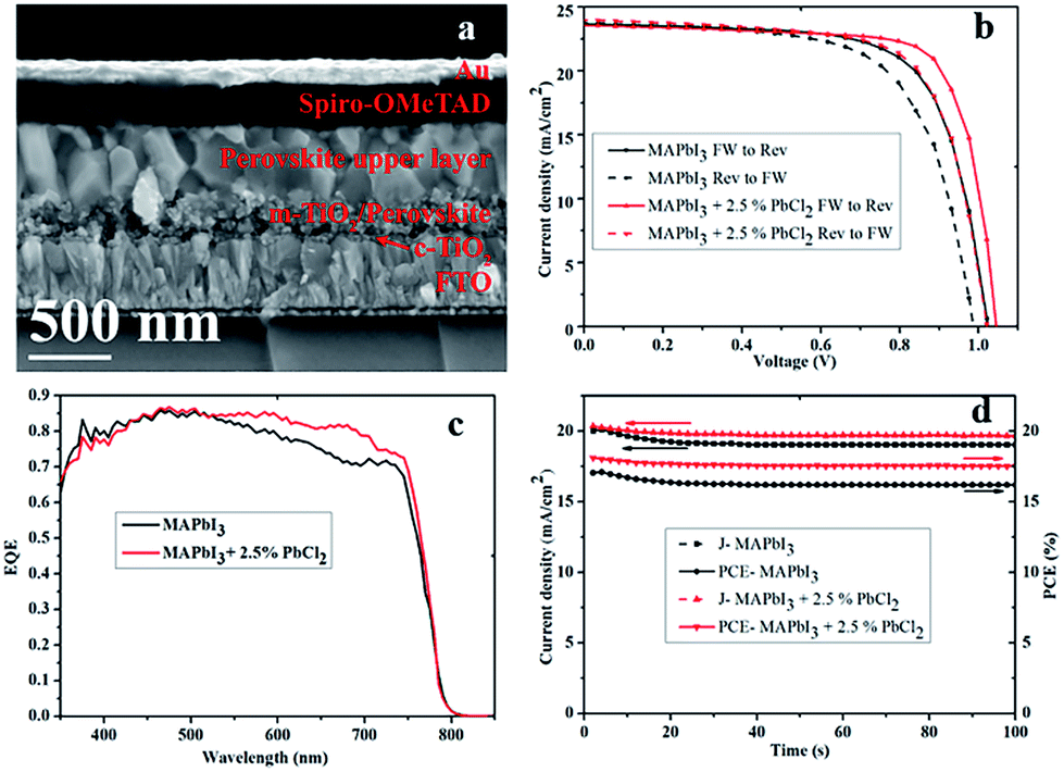 | ||
| Fig. 4 (a) Cross-sectional SEM image of the completed MAPbI3 + 2.5% PbCl2-additive solar cell; (b) J–V curves of perovskite solar cells using MAPbI3 with and without 2.5% PbCl2 in the perovskite precursor, under reverse and forward voltage scan; (c) corresponding IPCE spectra; and (d) steady-state photocurrent measured at a bias voltage (0.85 V for the MAPbI3 device and 0.89 V for the MAPbI3 + 2.5% PbCl2 device) at maximum power point and stabilized power output 10 s pre-conditioned to 1 sun light illumination. | ||
The J–V curves of the MAPbI3 perovskite solar cells with and without 2.5% of PbCl2 in the perovskite precursor measured under reverse (from Voc to Jsc) and forward (from Jsc to Voc) scanning are provided in Fig. 4b. The MAPbI3-based solar cell produces a PCE of 17.1 (15.1)%, with a Voc of 1.03 (0.98) V, a Jsc of 23.7 (23.8) mA cm−2, and a FF of 70 (65)% when measured under reverse (forward) scan, respectively, revealing a hysteresis (H) of 11.7% (H = 100% × (PCErev − PCEfw)/PCErev). In contrast, the MAPbI3–2.5% PbCl2-based solar cell achieved a PCE of 18.9 (17.2)%, a Voc of 1.05 (1.03) V, a Jsc of 23.7 (23.9) mA cm−2, and a FF of 76 (70)% when measured under reverse (forward) scan, respectively, with only 8.9% hysteresis.
The external quantum efficiency (EQE) spectra of the MAPbI3-based and MAPbI3–2.5% PbCl2-based device exhibit a high EQE value between 80% and 86% across a broad wavelength range from 400 nm to 750 nm with the photon response spectral tail extending to around 800 nm as illustrated in Fig. 4c. The integrated current densities are 20.1 mA cm−2 for the device with MAPbI3 and 20.8 mA cm−2 for the device with MAPbI3–2.5% PbCl2, which are slightly lower than those measured from J–V curves. This is ascribed to the presence of shallow trap states in the perovskite films. Shallow trap states in perovskite and/or interfaces can be easily filled under illumination during the J–V testing through very short light soaking (10 seconds in our case), which in turn facilitates charge carrier transport. However, the IPCE measurement was performed under very low intensity of monochromatic light without bias illumination. The electron generated in the IPCE measurement first needs to fill the trap states before being collected.27 This leads to a minor discrepancy in integrated Jsc from the IPCE spectrum as compared to the Jsc measured by constant steady-state illumination of the solar simulator.
The steady-state performance of the two representative cells (MAPbI3 and MAPbI3–2.5% PbCl2) at the maximum power point (MPP) was also measured (Fig. 4d). Both devices were pre-conditioned by illumination for 10 s prior to the measurement. The current densities at the MPP drop within a few seconds from 20.1 mA cm−2 to 19.1 mA cm−2 for the MAPbI3-based solar cell and from 20.4 mA cm−2 to 19.7 mA cm−2 for the MAPbI3–2.5% PbCl2-based solar cell under a continuous measurement duration of 100 s. The applied voltage bias near the MPP is 0.85 V for the MAPbI3-based device and 0.89 V for the MAPbI3–2.5% PbCl2-based device, which has a corresponding stabilized power output of 16.2% and 17.5%, respectively. This result suggests that addition of 2.5% PbCl2 into the perovskite precursor also dramatically improves the steady-state efficiency of PSCs.
The steady-state photoluminescence (PL) emission and time-resolved photoluminescence (TRPL) were carried out to elucidate the charge carrier dynamics of MAPbI3 and MAPbI3–2.5% PbCl2 films with and without the presence of charge transport layers (TiO2 and Spiro-OMeTAD) (Fig. 5(a)–(d)). Compared to the pristine MAPbI3 perovskite film, the intensity of the PL peak of the MAPbI3–2.5% PbCl2 film increases while the full width half maximum (FWHM) remains constant (Fig. 5a), indicating that more electron–hole pairs in the film lead to stronger radiative recombination. This indicates improved crystallinity of the as-deposited film.28 Moreover, the steady-state PL spectrum of the MAPbI3–2.5% PbCl2 film in Fig. 5a depicts a blue-shift by 2 nm (from 769 nm to 767 nm) which is consistent with the blue-shift observed in UV-vis absorption spectra acquired for the films, further suggesting the incorporation of chloride into the MAPbI3 lattice. On contacting with charge transport layers, a considerable decrease in PL intensity was observed. Compared to MAPbI3, the drop of PL peaks of MAPbI3–2.5% PbCl2 is more significant when in contact with the TiO2 film, suggesting a more efficient interfacial charge transfer. This is in good agreement with the enhanced performance of MAPbI3–2.5% PbCl2-based PSCs compared to pristine MAPbI3 devices.
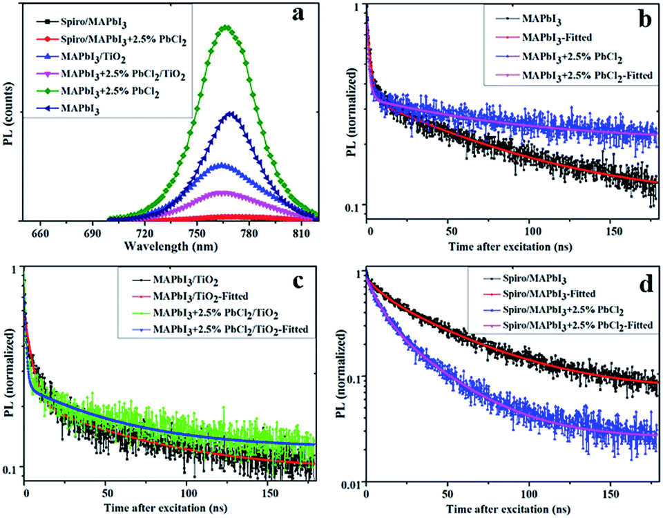 | ||
| Fig. 5 (a) Steady-state photoluminescence (PL) and normalized time-resolved photoluminescence (TRPL); (b) perovskite; (c) perovskite/TiO2; and (d) Spiro-OMeTAD/perovskite. | ||
The TRPL spectra of samples are fitted using a bi-exponential function of time (t) (F(t) = ∑aie−t/τi, i = 1, 2), which contains a fast decay time component and a slow decay time component.29 The fast decay component is associated with recombination behavior at the surface, while the slow decay component corresponds to recombination in the bulk of the perovskite film.30 The result indicates that, compared to pristine MAPbI3, addition of PbCl2 into the perovskite precursor results in films with a marginal decrease in the fast decay component (from 2.1 ns to 1.44 ns) but longer in the slow component of lifetime (from 80 ns to 85 ns) (Fig. 5b). Therefore the overall average PL lifetime of the perovskite layer is increased from 75 ns to 80 ns.
Time-resolved photoluminescence measurements of the MAPbI3 show a decrease in the PL lifetime of the perovskite layer from 75 ns to 56.7 ns in the presence of TiO2 (40 nm compact TiO2/200 nm mesoporous TiO2). When in contact with Spiro-OMeTAD, the lifetime = 45 ns is obtained. Whereas the PL lifetime of the MAPbI3–2.5% PbCl2 layer is reduced more significant from 80 ns to only 49.5 ns and 26.3 ns, respectively, when in contact with the TiO2 film and with Spiro-OMeTAD layer, indicating a faster and more effective electron and hole transport. The more effective hole transport is crucial for MAPbI3 perovskite due to the unbalanced electron–hole diffusion length (∼130 nm for electrons, ∼90 nm for holes) according to a previous report.20 These results indicate improved charge collection efficiency of MAPbI3–2.5% PbCl2-based PSCs compared to that of pristine MAPbI3, which is consistent with the improved FF of devices fabricated in this study.
To further explore the possible origin of the superior optoelectronic properties of the MAPbI3–2.5% PbCl2 based solar cell to the pristine MAPbI3 based solar cell, electrochemical impedance spectroscopy (EIS) measurements were conducted and the corresponding Nyquist plots are depicted in Fig. 6. The intercept point at the real part of the Nyquist plots is associated with series resistance of the device (Rs), which is mainly contributed to the sheet resistance of FTO glass. The small semicircle at high frequency corresponds to the charge transfer process between perovskite and selective contacts while the large semicircle at low frequency demonstrates the recombination of charge carriers in the perovskite layer (according to previous reports).31,32 Fitting the EIS of the MAPbI3 and MAPbI3–2.5% PbCl2 solar cells using an equivalent circuit depicted in the inset in Fig. 6 indicates that both devices have comparable interfacial charge transport behavior. Nevertheless, the MAPbI3–2.5% PbCl2 based solar cell has nearly 2.4-times higher resistance for recombination (1.68 × 10⁵ Ω) than the pristine MAPbI3 solar cell (6.93 × 10⁴ Ω), whereas both devices exhibit similar capacitance (0.789 μF for MAPbI3versus 0.769 μF for MAPbI3–2.5% PbCl2). As a result, the electron lifetime, a product of resistance and capacitance (τ = R × C), of the solar cell with the 2.5% PbCl2-additive in the precursor (τr = 0.12 s) is over 2-fold higher than the device made from pure MAPbI3 (τr = 0.055 s). The increased carrier lifetime is one of the factors that are responsible for the higher performance of the solar cell.
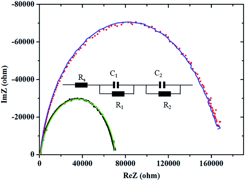 | ||
| Fig. 6 Nyquist plots of PSCs based on pristine MAPbI3 perovskite (square black) and fitting (green), and MAPbI3–2.5% PbCl2 perovskite (dot red) and fitting (blue) in the dark at 0.5 V forward bias. The inset depicts the corresponding equivalent circuit. | ||
Kelvin probe force microscopy (KPFM) is a powerful technique not only to examine surface topography but also the work function of the surface. The KPFM topography of both pristine MAPbI3 and MAPbI3–2.5% PbCl2 is shown in Fig. 7a and c. It appears that the surface of both perovskite films is uniform over a large area (5 × 5 μm2). However, the film made from the 2.5% PbCl2 based precursor consists of larger grains. The root mean square as an indicator of roughness of the film is 15.75 nm for the PbCl2-additive film and 14.27 nm for the pristine MAPbI3 film. The slightly rougher surface is attributed to its larger grain size. Measurement of the surface potential spectra of MAPbI3 and MAPbI3–2.5% PbCl2 films (Fig. 7b and d) reveals an increase of mean values of contact potential difference (CPD) by ∼90 mV in the MAPbI3–2.5% PbCl2 film compared to the MAPbI3 film. It is known that the conduction band of MAPbI3 perovskite is ∼80 meV more negative than that of n-type TiO2, which in principle forms an energy barrier for electron injection from MAPbI3 to n-TiO2 during the charge transport process.33 Therefore, the increase of the electron quasi-Fermi level near the conduction band edge of MAPbI3–2.5% PbCl2 favors improved energy level alignment with adjacent TiO2 for electron transfer at the MAPbI3–2.5% PbCl2/n-TiO2 interface. This work provides new insight into the mechanism that governs the impact of PbCl2 on both morphology and electronic properties of the MAPbI3 film for high energy conversion efficiency.
 | ||
| Fig. 7 KPFM topography of the (a) MAPbI3/mp-TiO2/compact TiO2/FTO-glass film and (c) MAPbI3–2.5% PbCl2/mp-TiO2/compact TiO2/FTO-glass film; (b and d) corresponding contact potential difference (CPD) images. | ||
The stability of un-encapsulated perovskite solar cells based on MAPbI3 with and without 2.5% PbCl2 was tested by aging the device at the maximum power point (MPP) under constant illumination (100 mW cm−2) at room temperature in ambient air (RH% = 50–60%). It is found that both devices retained ∼65% power conversion efficiency after 80 minutes stability testing (Fig. 8). The above results suggest that the impact of the PbCl2 additive on the stability of the perovskite solar cells is negligible in this work.
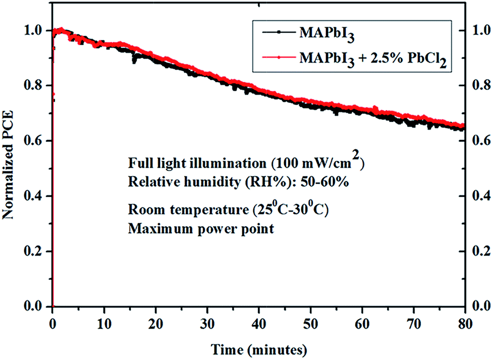 | ||
| Fig. 8 Relative performance of perovskite solar cells based on MAPbI3 with and without the 2.5% PbCl2 additive under continuous illumination for 80 minutes in ambient air with relative humidity: 50–60%. | ||
Conclusions
We have demonstrated the effect of PbCl2 on the morphology, crystallinity and recombination of the MAPbI3 perovskite film that was prepared via a one-step Lewis acid–base adduct method. Although addition of a low content of PbCl2 (less than 2.5%) into the MAPbI3 precursor did not pose a significant change in the crystal structure and optical properties, the resulting films show a larger grain size. More importantly, the PbCl2 additive improved the electronic properties and dynamics of charge carriers in the MAPbI3 film. The electronic properties of the perovskite film were modified by the PbCl2 additive with a significant downward shift of the surface work function by 90 meV, which facilitates electron injection from perovskite to TiO2. Analysis of TRPL indicated that the PbCl2-additive in the precursor led to perovskite films with a more balanced charge (electron and hole) collection and longer carrier lifetime. The EIS results of the corresponding PSCs also confirm that devices with the 2.5% PbCl2 additive have a 2.4-fold higher resistance for recombination compared to that in the pristine MAPbI3-based solar cell, indicating reduced trap density, resulting in a lower observed current–voltage hysteresis of solar cells. As a result, the performance of PSCs was increased from an average performance of 16.5% with pristine MAPbI3 to 18.1% with MAPbI3–2.5% PbCl2. The nearly 9% enhancement in device performance is mainly due to the improvement of the FF from 0.69 to 0.76.Acknowledgements
This work was supported by the Australian Research Council Future Fellowship (FT120100674) and Queensland-Chinese Academy of Science (Q-CAS) collaborative research fund. N. D. P. thanks Queensland University of Technology (QUT) postgraduate scholarship and CSIRO top-up scholarship. G. J. W. acknowledges funding support from CSIRO Research Office Julius Career Award and support of the CSIRO top-up scholarship for N. D. P. The data of XRD, SEM, and Ion Chromatography reported in this paper were obtained at the Central Analytical Research facility (CARF), QUT. Access to CARF was supported by the generous funding from Science and Engineering faculty, QUT. Dr Sunny Hu and her team at CARF are acknowledged for the Ion Chromatography measurement. In addition, we acknowledge the measurement of KPMS by Dr Kinnari Shelat at the Queensland node of the Australian national Fabrication Facility (ANFF), a company established under the National Collaborative Research Infrastructure Strategy.Notes and references
- A. Kojima, K. Teshima, Y. Shirai and T. Miyasaka, J. Am. Chem. Soc., 2009, 131, 6050–6051 CrossRef CAS PubMed.
- D. Bi, W. Tress, M. I. Dar, P. Gao, J. Luo, C. Renevier, K. Schenk, A. Abate, F. Giordano, J.-P. Correa Baena, J.-D. Decoppet, S. M. Zakeeruddin, M. K. Nazeeruddin, M. Grätzel and A. Hagfeldt, Sci. Adv., 2016, 2(1), e1501170 Search PubMed.
- M. Saliba, T. Matsui, J.-Y. Seo, K. Domanski, J.-P. Correa-Baena, M. K. Nazeeruddin, S. M. Zakeeruddin, W. Tress, A. Abate, A. Hagfeldt and M. Gratzel, Energy Environ. Sci., 2016, 9, 1989–1997 CAS.
- T.-B. Song, Q. Chen, H. Zhou, S. Luo, Y. Yang, J. You and Y. Yang, Nano Energy, 2015, 12, 494–500 CrossRef CAS.
- A. Binek, I. Grill, N. Huber, K. Peters, A. G. Hufnagel, M. Handloser, P. Docampo, A. Hartschuh and T. Bein, Chem.–Asian J., 2016, 11, 1199–1204 CrossRef CAS PubMed.
- S. Colella, E. Mosconi, G. Pellegrino, A. Alberti, V. L. P. Guerra, S. Masi, A. Listorti, A. Rizzo, G. G. Condorelli, F. De Angelis and G. Gigli, J. Phys. Chem. Lett., 2014, 5, 3532–3538 CrossRef CAS PubMed.
- S. T. Williams, F. Zuo, C.-C. Chueh, C.-Y. Liao, P.-W. Liang and A. K. Y. Jen, ACS Nano, 2014, 8, 10640–10654 CrossRef CAS PubMed.
- H. Yu, F. Wang, F. Xie, W. Li, J. Chen and N. Zhao, Adv. Funct. Mater., 2014, 24, 7102–7108 CAS.
- Y. Tidhar, E. Edri, H. Weissman, D. Zohar, G. Hodes, D. Cahen, B. Rybtchinski and S. Kirmayer, J. Am. Chem. Soc., 2014, 136, 13249–13256 CrossRef CAS PubMed.
- S. D. Stranks, G. E. Eperon, G. Grancini, C. Menelaou, M. J. P. Alcocer, T. Leijtens, L. M. Herz, A. Petrozza and H. J. Snaith, Science, 2013, 342, 341–344 CrossRef CAS PubMed.
- M. M. Lee, J. Teuscher, T. Miyasaka, T. N. Murakami and H. J. Snaith, Science, 2012, 338, 643–647 CrossRef CAS PubMed.
- G. E. Eperon, V. M. Burlakov, P. Docampo, A. Goriely and H. J. Snaith, Adv. Funct. Mater., 2014, 24, 151–157 CrossRef CAS.
- C. Huang, N. Fu, F. Liu, L. Jiang, X. Hao and H. Huang, Sol. Energy Mater. Sol. Cells, 2016, 145, 231–237 CrossRef CAS.
- B. Conings, J. Drijkoningen, N. Gauquelin, A. Babayigit, J. D'Haen, L. D'Olieslaeger, A. Ethirajan, J. Verbeeck, J. Manca, E. Mosconi, F. D. Angelis and H.-G. Boyen, Adv. Energy Mater., 2015, 5, 1500477 CrossRef.
- N. J. Jeon, J. H. Noh, Y. C. Kim, W. S. Yang, S. Ryu and S. I. Seok, Nat. Mater., 2014, 13, 897–903 CrossRef CAS PubMed.
- N. Ahn, D.-Y. Son, I.-H. Jang, S. M. Kang, M. Choi and N.-G. Park, J. Am. Chem. Soc., 2015, 137, 8696–8699 CrossRef CAS PubMed.
- C. Qin, T. Matsushima, T. Fujihara and C. Adachi, Adv. Mater., 2017, 29, 1603808 CrossRef PubMed.
- Z. Xiao, Q. Dong, C. Bi, Y. Shao, Y. Yuan and J. Huang, Adv. Mater., 2014, 26, 6503–6509 CrossRef CAS PubMed.
- P.-W. Liang, C.-Y. Liao, C.-C. Chueh, F. Zuo, S. T. Williams, X.-K. Xin, J. Lin and A. K. Y. Jen, Adv. Mater., 2014, 26, 3748–3754 CrossRef CAS PubMed.
- G. Xing, N. Mathews, S. Sun, S. S. Lim, Y. M. Lam, M. Grätzel, S. Mhaisalkar and T. C. Sum, Science, 2013, 342, 344–347 CrossRef CAS PubMed.
- D.-Y. Son, J.-W. Lee, Y. J. Choi, I.-H. Jang, S. Lee, P. J. Yoo, H. Shin, N. Ahn, M. Choi, D. Kim and N.-G. Park, Nature Energy, 2016, 1, 16081 CrossRef CAS.
- Y. Li, W. Sun, W. Yan, S. Ye, H. Peng, Z. Liu, Z. Bian and C. Huang, Adv. Funct. Mater., 2015, 25, 4867–4873 CrossRef CAS.
- H. Xu, Y. Wu, J. Cui, C. Ni, F. Xu, J. Cai, F. Hong, Z. Fang, W. Wang, J. Zhu, L. Wang, R. Xu and F. Xu, Phys. Chem. Chem. Phys., 2016, 18, 18607–18613 RSC.
- J. Chae, Q. Dong, J. Huang and A. Centrone, Nano Lett., 2015, 15, 8114–8121 CrossRef CAS PubMed.
- D. E. Starr, G. Sadoughi, E. Handick, R. G. Wilks, J. H. Alsmeier, L. Kohler, M. Gorgoi, H. J. Snaith and M. Bar, Energy Environ. Sci., 2015, 8, 1609–1615 CAS.
- B. Wang, K. Young Wong, X. Xiao and T. Chen, Sci. Rep., 2015, 5, 10557 CrossRef PubMed.
- T. Yokoyama, D. H. Cao, C. C. Stoumpos, T.-B. Song, Y. Sato, S. Aramaki and M. G. Kanatzidis, J. Phys. Chem. Lett., 2016, 7, 776–782 CrossRef CAS PubMed.
- C. Fei, J. Tian, Y. Wang, X. Liu, L. Lv, Z. Zhao and G. Cao, Nano Energy, 2014, 10, 353–362 CrossRef CAS.
- D. R. James, Y.-S. Liu, P. De Mayo and W. R. Ware, Chem. Phys. Lett., 1985, 120, 460–465 CrossRef CAS.
- Q. Dong, Y. Fang, Y. Shao, P. Mulligan, J. Qiu, L. Cao and J. Huang, Science, 2015, 347, 967–970 CrossRef CAS PubMed.
- H.-S. Kim, I. Mora-Sero, V. Gonzalez-Pedro, F. Fabregat-Santiago, E. J. Juarez-Perez, N.-G. Park and J. Bisquert, Nat. Commun., 2013, 4, 2242 Search PubMed.
- A. Guerrero, G. Garcia-Belmonte, I. Mora-Sero, J. Bisquert, Y. S. Kang, T. J. Jacobsson, J.-P. Correa-Baena and A. Hagfeldt, J. Phys. Chem. C, 2016, 120, 8023–8032 CAS.
- J. P. Correa Baena, L. Steier, W. Tress, M. Saliba, S. Neutzner, T. Matsui, F. Giordano, T. J. Jacobsson, A. R. Srimath Kandada, S. M. Zakeeruddin, A. Petrozza, A. Abate, M. K. Nazeeruddin, M. Gratzel and A. Hagfeldt, Energy Environ. Sci., 2015, 8, 2928–2934 CAS.
Footnote |
| † Electronic supplementary information (ESI) available. See DOI: 10.1039/c6ta11139d |
| This journal is © The Royal Society of Chemistry 2017 |