
 Open Access Article
 This Open Access Article is licensed under a
 Creative Commons Attribution 3.0 Unported Licence
Effect of oxidative surface treatments on charge storage at titanium nitride surfaces for supercapacitor applications†
Benjamin M.
Gray
a,
Andrew L.
Hector
 *a,
Marek
Jura
b,
John R.
Owen
a and
Joshua
Whittam
a
*a,
Marek
Jura
b,
John R.
Owen
a and
Joshua
Whittam
a
aChemistry, University of Southampton, Highfield, Southampton SO17 1BJ, UK. E-mail: A.L.Hector@soton.ac.uk
bISIS, STFC, Harwell Innovation Campus, Didcot, Oxfordshire OX11 0DE, UK
First published on 2nd February 2017
Abstract
The effects of surface oxidation on the capacitance of titanium nitride electrode surfaces, produced by reaction of titanium foils with ammonia, are examined. Thermal oxidation and electrochemical oxidation both increase the amount of redox active oxide at the surface, but electrochemical oxidation is found to be more successful in increasing the capacitance.
Introduction
Supercapacitors store charge at the interface between an electrode and an electrolyte. Initially they were used to provide backup power to electronic components, but now find applications ranging from cells used to produce small amounts of energy in fast pulses, to fast recharging power tools and cells of more than 100 kF to recover kinetic or potential energy in buses and cranes.1 Increasingly they will be used in vehicles, where a battery or fuel cell will provide high density energy storage and a supercapacitor the high power density required for hill climbing and rapid acceleration.2 Most research in supercapacitors is concerned with devices that rely on high surface area electrodes, typically carbon, and store charge in a thin double layer of anions and cations very close to the surface.There is an increasing interest in electrodes that can also undergo surface redox processes and hence increase the amount of charge that they can store. These devices are referred to as redox supercapacitors, or pseudo capacitors, since they combine the functions of capacitors with those of batteries.1–3 Metal oxides and conducting polymers have been used extensively as the active materials in redox supercapacitors.4 The current leading material is hydrous ruthenium oxide, which combines good electronic conductivity with good transport of protons in the hydrous surface layers and a theoretical charge storage capacity of 1358 F g−1.5 Capacitances approaching this theoretical value have been achieved in composites with 10–20% RuO2 loading on carbon,6 and even at high rates of 1 V s−1 with structured electrodes such as nanotube arrays.7 However, these approaches suffer from fading capacity with increased loading or a high processing cost, respectively, and the material cost in use of RuO2 is also an issue.
Metal nitrides including TiN,8–14 VN,15–22 NbN,23 Nb4N5,24 Mn3N2,25 Mo2N,26–29 RuN30 and WN31 have been investigated for supercapacitor applications. Notably Choi et al. found that nanocrystalline VN could deliver a specific capacity of 1340 F g−1 at 2 mV s−1 scan rate in aqueous KOH electrolyte.15 The advantage of metal nitrides in supercapacitor electrodes is that in most cases they have much higher electronic conductivities than the respective oxides. In VN the capacity increased over initial cycles as a layer of oxide formed, and the high capacity was attributed to redox processes in this surface oxide layer.15 More recently this principle of a conductive core metal nitride with a redox active surface has been expanded with TiN nanostructures used to provide current collectors for MnO2,32 RuO2,33 VN34 and graphene35 redox materials.
However, TiN has also generated a growing interest in its use without a separate redox component. Initial studies showed that the capacitance of electrodes based on nanocrystalline TiN decreased during cycling as surface oxide formed.9 With larger crystallites the capacitances were lower but were maintained much better during cycling.9,10 Recently the focus has moved to structures with continuous electronic pathways, e.g. TiN nanopore structures produced by anodization methods have delivered a stable capacitance of 27.59 mF cm−2,12 mesoporous TiN films have achieved over 200 F g−1 capacitance,14 and supported TiN “corn-like” structures had high volumetric capacity of 1.5 mW h cm−3.11 Interestingly the latter study showed an increase in capacitance during cycling that was attributed to “surface activation”. Achour et al. were able to link the performance of the native oxide surface directly to its nitrogen content and show that nitrogen-rich TiN retains capacity more effectively due to nitrogen doping of this surface oxide that enhances its conductivity.13 Titanium oxynitride nanostructures have also shown good supercapacitor performance.36 In view of these studies and other recent work using TiN as the shell in core–shell supercapacitor structures,37–39 there is a significant need to understand how the formation of surface oxide affects the electrochemical behaviour of TiN surfaces. Herein we have applied various oxidation treatments to low area titanium nitride surfaces and linked their charge storage capacity to a detailed characterisation of the electrode surfaces. The resultant insights are intended to be transferable to high surface area titanium nitride electrodes.
Experimental
TiN electrodes were prepared from titanium foil (99.96%, 0.25 mm thick, Goodfellow), which was cut into flag shapes with a 10 × 10 mm square plus a strip of metal protruding for electrical connection. The electrodes were cleaned by sonication for 30 minutes each in acetone and deionized water and then blown dry with nitrogen. These were heated under anhydrous ammonia (BOC) in an alumina crucible contained in a quartz furnace tube using a modified literature method,40 taking care to ensure that all metal surfaces were placed such that they were well exposed to the gas environment. The electrodes were heated at 550 °C for 30 minutes then the temperature was raised at 2 °C min−1 to 1000 °C, maintained for 10 hours and allowed to cool naturally in the ammonia flow. Some TiN foils were removed from the furnace at room temperature and stored in air, these are referred to as “as prepared” or “untreated” foils. Others were oxidised with the intention of producing a thicker surface corrosion layer, either:• “Thermally oxidized” (TO) by heating in air for 24 h at temperatures between 250 and 450 °C.
• “Cyclic voltammogram oxidized” (CVO) by ramping their potential from 0 to 1.2 V vs. Hg/HgO and back 10 times at 100 mV s−1 in 6 mol dm−3 KOH. Samples were then rinsed with deionised water, allowed to dry and stored in air.
• “Potential step oxidized” (PSO) by maintaining a fixed potential in the range 0.5–2.0 V vs. Hg/HgO for a period of 50 to 200 s in 6 mol dm−3 KOH. Samples were then rinsed in deionised water, allowed to dry and stored in air.
Grazing incidence X-ray diffraction data (XRD) were collected using a Rigaku Smartlab diffractometer with a parallel beam of Cu-Kα X-rays, incidence angles between 0.5 and 5° and a DTex250 1D detector. Rietveld refinement was carried out using the GSAS package.41,42 Atomic force microscopy (AFM) was conducted using a Veeco Dimension 3100 instrument in tapping mode. Scanning electron microscopy (SEM) used a Jeol JSM5910 microscope. Energy dispersive X-ray spectroscopy (EDX) measurements were carried out with a Thermofisher Ultradry detector using a 15 kV accelerating voltage, and wavelength dispersive X-ray spectroscopy (WDX) with a Thermofisher Magnaray detector and a 5 kV accelerating voltage, both mounted on a Philips XL-30 ESEM.
X-ray photoelectron spectra (XPS) were recorded using a Scienta ESCA300 with an Al Kα (1486.7 eV) source and a 90° take-off angle used in most cases. Some samples were etched using argon ion bombardment for 20 minutes at 4 keV. The Ti 2p, N 1s, C 1s and O 1s spectra were collected. The CASA XPS 2.3.15 software package was used for data analysis. Metal 2p doublets were modelled with constrained relative intensities of the 2p3/2 and 2p1/2 peaks (3![[thin space (1/6-em)]](https://www.rsc.org/images/entities/char_2009.gif) :1) and separation of these peaks based on initial modelling of data for Ar+ ion etched TiN. The asymmetric peak shape was based on that reported in a previous study of TiN.43 Data was referenced to the adventitious carbon 1s peak, which was assigned a binding energy of 284.8 eV, or to the argon 2p3/2 at 241.6 eV after etching where carbon 1s was not present.
:1) and separation of these peaks based on initial modelling of data for Ar+ ion etched TiN. The asymmetric peak shape was based on that reported in a previous study of TiN.43 Data was referenced to the adventitious carbon 1s peak, which was assigned a binding energy of 284.8 eV, or to the argon 2p3/2 at 241.6 eV after etching where carbon 1s was not present.
Electrochemical measurements were conducted using Bio-Logic VMP2 or SP-150 potentiostats. The aqueous 1 mol dm−3 electrolytes were deoxygenated by bubbling nitrogen through them and all potentials are quoted relative to Hg/HgO in 0.1 M NaOH, which has a potential of 0.10 V vs. SHE.44 Capacitance measurements used cyclic voltammograms collected with a potential window chosen (after initial experiments) to avoid solvent decomposition. A sequence of scan rates was applied, with 10 scans each at 1000, 1, 5, 10, 50, 100 and 500 mV s−1 and then 100 scans at 1000 mV s−1. The middle (5th or 50th) scan at each rate was used for capacitance calculations and plotted CVs. Areal specific capacitance was calculated as half of the integral of the CV (mA V) trace divided by (scan rate (mV s−1) × the width of the potential window (1.1 V) × area of the film (cm2) exposed to the electrolyte). Galvanostatic experiments were performed after 180 scans of cyclic voltammetry as described above, with currents of 0.033, 0.1, 0.33, 1.0 and 3.3 mA and fixed potential limits. Electrochemical impedance spectroscopy (EIS) measurements were made at the open circuit potential after all other electrochemical treatments, with a frequency range of 1 MHz to 10 mHz and an amplitude of 10 mV, and EIS data were fitted using ZView.45
Results and discussion
Electrodes were initially prepared by heating flag-shaped pieces of titanium foil in ammonia. After nitridation the electrodes exhibit the golden colour usually seen in TiN films produced by physical vapour deposition and retain metallic conductivity, with a resistance of 2.5 mΩ measured along the 2 cm length of a flag-shaped electrode (2-point resistance measurement, so this value includes the resistance of the leads and contacts).Grazing incidence X-ray diffraction measurements were carried out to determine which phases were present at the surface of the electrodes. Absorption of 50% of photons will occur at a path length of 8 μm in TiN,46 and this path length is equivalent to a depth normal to the surface of 0.7 or 0.07 μm with an incident angle of 5 or 1°, respectively. The as-prepared metal nitride foils exhibited strong peaks corresponding to rocksalt-structured TiN (Fig. 1). Rietveld refinement of the data collected at 5° incidence resulted in lattice parameters of 4.22857(13) Å for TiN (Fig. S1†). This is close to the literature values, which range between 4.23–4.27 Å for TiN.47 Further peaks are also observed, although these are weaker at lower incidence angles relative to the TiN peaks indicating that they are due to phases present below the surface. These secondary peaks also showed strong texturing (spotty diffraction rings when collected with an area detector) suggesting large crystallites. Phase matching identified these peaks as due to “TiN0.3” and “Ti2N”,48 which are both disordered alloy phases with the hexagonal titanium structure. A survey of the phases in the ICSD and PDF databases showed that these phases show a clear Vegard trend in the cell volume with nitrogen content (Fig. S2†),47,48 and from this the two sub-surface phases can be estimated to have compositions of TiN0.29 (volume = 37.155(4) Å3) and TiN0.47 (volume = 38.357(8) Å3).
 | ||
| Fig. 1 Grazing incidence XRD patterns for titanium nitride foils collected at incidence angles as shown. The Miller indices of the cubic rocksalt-type TiN47 peaks are labelled, and the remaining peaks are due to hexagonal titanium nitride phases. | ||
Scanning electron microscopy shows fairly smooth metallic surfaces on the as-prepared TiN foils (Fig. S3†), with no obvious changes on this length scale in those that had undergone surface treatment. EDX measurements showed 51% N and 49% Ti, with oxygen contents <1%. This sampling depth for EDX is around 1 μm, so this supports the evidence from variable incidence angle measurements (Fig. 1) that the nitrogen deficient phases observed in the XRD are below the surface of the foils. AFM data collected to observe the roughness on shorter length scales show some surface roughness on the as-prepared TiN foils and allow the real surface area of the electrodes to be measured (Fig. 2).
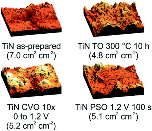 | ||
| Fig. 2 AFM images of titanium nitride foil surfaces, as prepared or with oxidation treatments as shown. Surface areas are in cm2 per cm2 of electrode area. AFM images were collected on a 1 × 1 μm region of the electrode surface and the images are displayed with a 1 × 1 × 1 μm scale. | ||
XPS is inherently surface sensitive as photoelectrons can only escape from within a few nm of the surface, and hence is particularly relevant in understanding the layer of material that will be in direct contact with the electrolyte. The Ti 2p XPS spectrum of as-prepared TiN foils showed three overlapping doublets (Fig. 3). Based on the work of Saha et al.,49 those with binding energies of 455 and 461 eV (2p3/2 and 2p1/2 respectively) were assigned as TiN (i.e. roughly Ti3+) and those at 459 and 464.5 eV as TiO2 (Ti4+), whereas broader peaks in between were assigned as Ti(O,N) species (Table 1), with the greater breadth of these intermediate signals attributed to a range of possible environments.43 Other recent studies of TiN for supercapacitor applications have found very similar surface environment distributions and used similar assignments of the peaks.11,13,36 Reduction of the take-off angle results in reduction of the TiN signal and enhancement of the TiO2 signal, suggesting that even within this thin surface film there is some variation in the composition with the most oxide-rich component closest to the surface. Ar+-ion etching reduced the contribution from Ti(O,N) from 26% to 3% and the TiO2 contribution from 33% to an undetectable level, suggesting that the majority of the oxide was present in a thin passivation layer. A strong shake up peak43 was also observed in these heavily etched samples, coincident with the position of the Ti(O,N) 2p3/2 peak.
 | ||
| Fig. 3 The Ti 2p region of the XPS spectra for un-etched TiN foils as-prepared and after application of various oxidative treatments as indicated. The TiN peaks are highlighted in green, Ti(O,N) in red and TiO2 in purple. The yellow region in the as-prepared sample is a shake-up peak. | ||
| Sample | BE TiN (eV) | % | BE Ti(O,N) (eV) | % | BE TiO2 (eV) | % |
|---|---|---|---|---|---|---|
| a TiN shake-up43 peak (3%) also included in as-prepared data fit. | ||||||
| TiN as prepareda | 455.1 | 38 | 457.4 | 26 | 458.9 | 33 |
| TiN TO 300 °C 10 h | 454.8 | 21 | 456.5 | 37 | 458.4 | 42 |
| TiN CVO 10× 0 to 1.2 V | 453.9 | 3 | 456.5 | 10 | 458.3 | 87 |
| TiN PSO 1.2 V 100 s | 454.6 | 3 | 456.6 | 8 | 458.6 | 89 |
Characterisation of TiN surfaces after surface oxidation
Surface oxidations were carried out either by heating the TiN foils in air or by ramping their potential to values positive of those at which the aqueous KOH electrolyte started to oxidise. Previously we showed that the interface resistance at a TiN surface increases above ∼350 °C,50 so the expectation was that a very thin oxide layer would be produced at ∼300 °C. The effect of surface oxidation during cyclic voltammetry within the potential window in which the electrolyte was stable (typically −0.8 to +0.3 V vs. Hg/HgO herein) will be observed during cycling of the as-prepared electrodes. To produce thicker electrochemical oxidation layers the potential was raised to +1.2 V (vs. Hg/HgO), either in 10 CV cycles up to this potential or by holding for a period of time. No changes to the surfaces were observable by XRD or SEM, but AFM of electrodes oxidised using these thermal and electrochemical oxidation procedures showed that in all cases the surfaces became a little smoother (Fig. 2). These AFM measurements have been used to calculate areal specific capacitances based on the real surface areas of the electrodes.XPS studies of oxidised electrodes were carried out without etching to obtain a direct comparison between the surfaces after the various surface treatments, focussing on the Ti 2p spectra so that the data reflected the surface composition rather than adsorbed species. Fig. 3 shows the fitted data and Table 1 lists the compositions in terms of the various surface species observed. Thermal oxidation increases the amount of Ti(O,N) and TiO2 at the surface with a matching reduction in the TiN content, but these are relatively subtle changes compared with those observed in electrochemical oxidation. Both the potential step and the cyclic voltammetry oxidation processes result in the surface being dominated by species with binding energies consistent with TiO2 (or Ti4+).
Effect of thermal oxidation on capacitance
Cyclic voltammograms of the as-prepared TiN electrode in aqueous KOH electrolyte showed a typical capacitive “letter-box” shape at high scan rates (Fig. 4), with an exponential decay behaviour at the current reversal regions that is characteristic of series resistance. Aqueous KOH has frequently been used in charge storage with TiN8–10 and herein was found to give higher capacitances than acidic or neutral electrolytes. Superimposed onto this shape the current is seen to gradually tail downwards at low potential and a broad, low peak is observed on re-oxidation, with the voltage envelope broadened due to the reliance of the (presumably Ti3+/Ti4+) redox chemistry on proton diffusion through the surface layer. It may also be the case that the currents are generally higher at low potentials because reduction of some of the titanium ions at the surface enhances the electronic conductivity in this region. The electrochemical stability window was originally assessed by running CVs over various potential ranges to avoid solvent decomposition, and the 1.1 V range is wider than in many other studies9,13,36 and closer to the limits of the water window (−0.93 to +0.30 V vs. Hg/HgO based on standard electrode potentials51). At high potential a small upturn in the current is observed in the positive sweep, which may contain a small solvent oxidation contribution. The bulk of this upturn is likely to be due to electrode oxidation since with further cycling (Fig. S4–S9†) the upturn becomes minimal. Note that the potential hysteresis in this region of the CV is narrower than the average across the CV, so this feature does not result in an increase in the calculated capacitance relative to that measured with a smaller potential window. | ||
| Fig. 4 (a) Cyclic voltammograms in 1 mol dm−3 KOH (5th cycle at 1000 mV s−1) of as-prepared and thermally oxidised TiN samples, and (b) areal specific capacitance values at the 5th cycle at each of the sequential scan rates. TO250, TO300, TO350, TO400 and TO450 represent oxidation at 250, 300, 350, 400 and 450 °C respectively. | ||
Based on the AFM-measured surface area, the areal specific capacitance of the as-prepared TiN electrode in the 5th cycle at 1000 mV s−1 was 30.7 μF cm−2 (often such values are quoted based on the electrode area without a correction for the surface area of the material, and on this basis the areal specific capacitance would be 215 μF cm−2). CVs were recorded at a series of rates and the capacitance calculated at the middle scan at each rate, with the largest capacitance of 915 μF cm−2 found in the 5th scan at the slowest scan speed of 1 mV s−1. After further sets of 10 scans each at 5, 10, 50, 100 and 500 mV s−1 (Fig. S4–S9†) the capacitance in the 50th scan at 1000 mV s−1 (Fig. S10†) was 35.1 μF cm−2. A small increase in capacitance has thus been observed during electrochemical cycling of TiN within the electrochemical window in which the aqueous 6 mol dm−3 KOH electrolyte was stable, but this is quite limited over the 170 cycles at various scan rates carried out here.
Thermal oxidation was carried out at temperatures between 250 and 450 °C, over which range the interface resistance of TiN has previously been shown in organic electrolyte to increase from a few ohms to megaohms.50 No increases in capacitance relative to the as-prepared samples were observed in the thermally oxidised samples during the initial cycles at any scan rate (Fig. 4). This observation persisted in the slower scans, apart from in the sample produced at the lowest temperature of 250 °C, in which the areal specific capacitance gradually increased during cycling to a larger capacitance value than the as-prepared sample of 92.2 μF cm−2 in the final 1000 mV s−1 cycles. Here a significant imbalance in the oxidation vs. reduction charge passed during the cyclic voltammetry (e.g. 0.0012 and 0.0009C in the 5th cycle at 5 mV s−1) suggests some further oxidation of the surface is linked to the development of further capacity. By the end of cycling these values come close to convergence, with a small excess oxidation charge probably attributable to the observed water oxidation at the highest potentials. The XPS data in Fig. 3 show that an increase in the oxide content of the surface is produced by thermal oxidation. This surface oxide could increase the capacitance by providing a dielectric layer as found in electrolytic capacitors1 or by undergoing redox reactions. It is noteworthy that in the as-prepared sample and those with thicker oxide layers the log capacitance vs. log scan rate plot (Fig. 4) has a slope close to −1/2 at low scan rate suggesting capacity is diffusion limited52 (i.e. it has a significant redox component reliant on solid state diffusion) and is flatter at high scan rate suggesting mainly double layer capacitance. The samples produced at 250 and 300 °C have a much flatter profile overall, presumably due to the changing capacitance as the surface changes as described above.
The reduction in capacity and increase in resistance seen in most thermally oxidised samples could suggest that the thin (according to XPS) oxide layer produced under these conditions is dense with low ionic and electronic conductivity (this could contribute to capacitance by providing a surface dielectric layer). The development of higher capacitance values during cycling in the thinnest of these could be due to ion doping of the layer and further oxidation as the potential is cycled in the aggressive aqueous KOH electrolyte.
Effect of electrochemical oxidation on capacitance
Initial cyclic voltammetry studies based on the samples used for XPS and AFM showed that potential step oxidation had a larger effect on the capacitance than cyclic voltammetry up to the same potential, presumably because the time spent at the maximum potential was greater. The XPS and AFM showed both techniques produced similar surfaces. Hence a more detailed assessment of the benefits of electrochemical oxidation was carried out using the potential step method.Potential step oxidations were carried out in 6 mol dm−3 aqueous KOH at 1.2 V (vs. Hg/HgO) for periods between 50 and 200 s, and also for 100 s at potentials between 0.5 and 2.0 V (vs. Hg/HgO). Cyclic voltammograms (Fig. S11–S17† and 5) were similar in shape to those observed after thermal oxidation, and were recorded over the same series of scan rates (10 scans each at 1000, 1, 5, 10, 50, 100, 500 mV s−1 then 100 scans at 1000 mV s−1). In the initial scans at 1000 mV s−1 most of the oxidised electrodes had no increase in areal specific capacitance relative to the as-prepared TiN. However, in the scans at 1 mV s−1 and in subsequent scans significant changes in capacitance were observed. The samples produced at 1.2 V vs. Hg/HgO all had higher capacitance, with 2170 μF cm−2 in the sample oxidised for 150 s (11100 μF cm−2 based on geometric electrode area). These increases could be due to thickening of the oxide layer or to further ion doping. At fast scan rates after cycling the increase in capacitance observed in one of the thermally oxidised samples was observed in all of the potential step oxidised samples. The largest capacitances at 1000 mV s−1 were found in the samples that had been produced at less positive potentials, with 83.1 μF cm−2 in the sample oxidised at 1.0 V vs. Hg/HgO for 100 s (424 μF cm−2 based on geometric electrode area), increasing from a value of 34.9 μF cm−2 before cycling. An extended cycling study (5000 cycles) on one such electrode at 1000 mV s−1 showed that the capacitance gradually increased by a further 13% over the first 1200 cycles, then gradually decayed to a value 3% higher than the value at the start of the 5000 cycles by the end of the 5000 cycles (Fig. S18†). Hence these electrodes show good stability.
Galvanostatic charge/discharge measurements were performed on three electrodes after the cyclic voltammograms shown in Fig. 5 (CVs were carried out first to ensure full development of the oxide surface). This process was carried out with an untreated electrode and with electrodes that had originally been potential step oxidised at 1.2 V for 150 s and at 1.0 V for 100 s. These treatments were chosen because in the CV measurements those electrodes exhibited strong charge storage characteristics at slow and fast scan rates (respectively). Galvanostatic cycling was performed with potential limits of −0.8 V to 0.2 V at currents ranging from 0.033 to 3.3 mA. At slow scan rates some irreversible current was passed due to solvent oxidation at the top of the potential range. This galvanostatic mode contributes to an increase in the measured capacitance (unlike in the CVs as noted above) as the current consumed by solvent oxidation reduces the slope of the current/time curve. Hence to avoid this effect the discharge curves (Fig. 6) were used to calculate the areal capacitance shown in Table 2. The currents used correspond roughly, in terms of the time taken during discharge, to CV scan rates between 10 and 1000 mV s−1. The capacitance increases seen in the CVs in potential step oxidised samples are also seen in the galvanostatic discharge capacitances, and the capacitance values are comparable.
 | ||
| Fig. 5 (a) Cyclic voltammograms in 1 mol dm−3 KOH (50th cycle of the final set at 1000 mV s−1) of the of as-prepared and potential step oxidized TiN, and (b) areal specific capacitance values at the middle cycle of each of the sequential scan rates of PSO1.2 V50 s, PSO1.2 V100 s, PSO1.2 V150 s and PSO1.2 V200 s were oxidised at 1.2 V for 50 s, 100 s, 150 s and 200 s respectively and PSO0.5 V100 s, PSO1.0 V100 s, PSO1.5 V100 s and PSO2.0 V100 s were oxidised for 100 s at 0.5 V, 1.0 V, 1.5 V and 2.0 V respectively. | ||
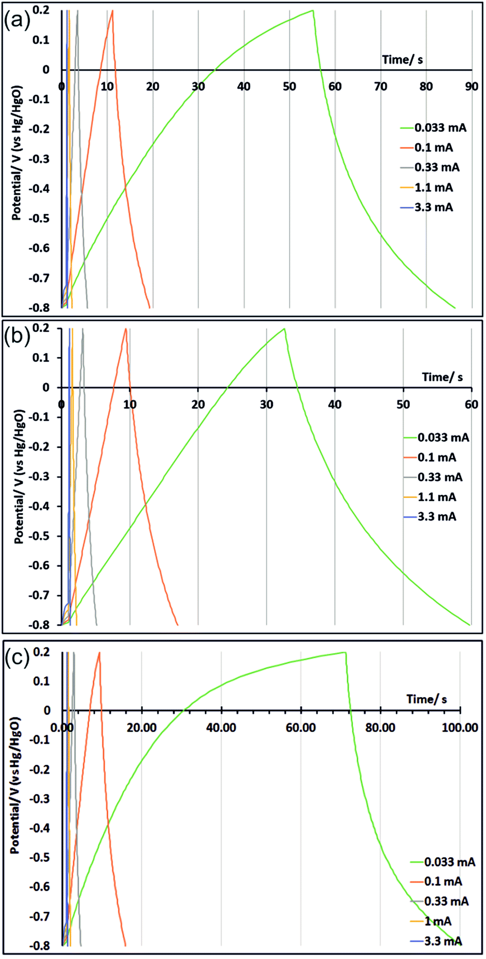 | ||
| Fig. 6 Galvanostatic cycling, carried out after 170 cycles cyclic voltammetry as shown in Fig. 5, of untreated TiN (a), TiN potential step oxidised at 1.2 V for 150 s (b) and TiN potential step oxidised at 1.0 V for 100 s (c). | ||
| Current/mA | 0.033 | 0.1 | 0.33 | 1.0 | 3.3 |
| Capacitance untreated/μF cm−2 | 61.9 | 55.5 | 50.4 | 45.9 | 41.8 |
| Capacitance PS1.2 V150 s/μF cm−2 | 73.7 | 70.0 | 64.4 | 58.7 | 53.0 |
| Capacitance PS1.0 V100 s/μF cm−2 | 99.3 | 81.7 | 72.4 | 65.3 | 64.5 |
The same three samples were subjected to EIS at the open circuit potential after the galvanostatic cycling. The Nyquist plots (Fig. 7) were fitted with an equivalent circuit consisting of a parallel constant phase element/resistor combination in series with a further resistance. These represent the interface capacitance/resistance and the series resistance (respectively). The untreated electrode was found to have a capacitance of 625(3) μF (44.6 μF cm−2), a parallel resistance of 34.0(8) kΩ and a series resistance of 1.657(7) Ω. The potential step oxidised sample treated at 1.2 V for 150 s had a capacitance of 502.1(11) μF (49.2 μF cm−2), a parallel resistance of 88(2) kΩ and a series resistance of 1.920(5) Ω. The sample oxidised at 1.0 V for 100 s had a capacitance of 585(4) μF (57.6 μF cm−2), a parallel resistance of 48(3) kΩ and a series resistance of 1.438(15) Ω. The parallel resistance (representing charge leakage due to oxidation) can be observed to have increased with oxidation time as the oxidation layer thickens. The areal capacitance was increased by potential step oxidation as expected, with the highest value found in the sample oxidised at 1.0 V for 100 s. Plotting capacitance vs. frequency (Fig. 7), this electrode can be seen to have the highest capacitance across the frequency range. The sloping capacitance profiles with the highest values at low frequency show that even at the open circuit potential, where these measurements were carried out, some redox capacitance is operating and the redox reactions are reversible. Above 100 Hz the plot of log of the capacitance vs. the log of the frequency falls rapidly due to the dominance of the series resistance effect compared with the capacitive impedance at high frequency. In this frequency range the phase angle also drops. Fitted spectra can be found in Fig. S19–S21.†
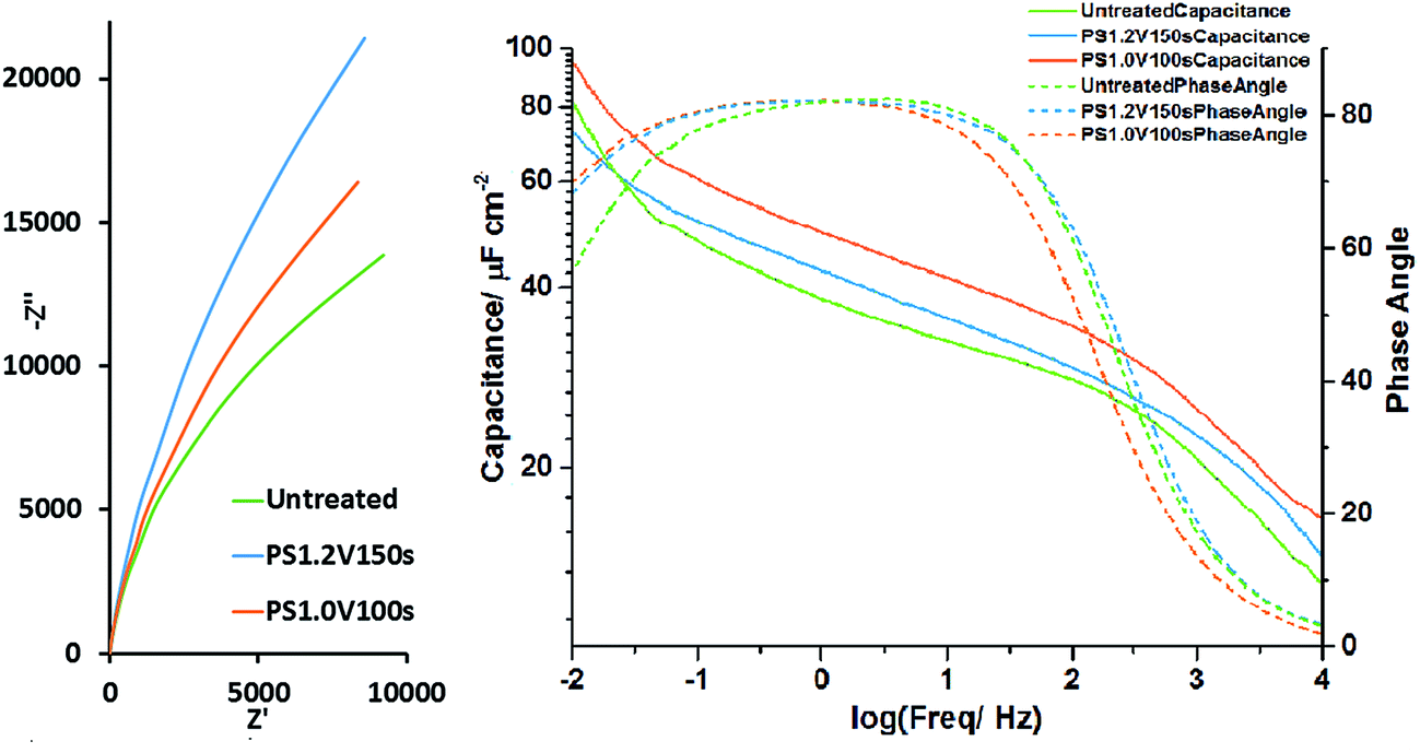 | ||
| Fig. 7 Nyquist plot of the EIS (left) and areal capacitance vs. frequency plot (right) of untreated TiN, PS1.2 V150 s and PS1.0 V100 s electrodes collected at the open circuit potential (∼−0.4 V). | ||
XPS measurements on a potential step oxidised foil (Fig. 3) showed the surface to contain mainly oxide or Ti4+ environments at the sampling depth of the technique, approximately 10 nm. EDX or WDX can sample at greater depth and, at typical accelerating voltages of between 10 and 20 kV, a ballpark figure of 1 μm is often quoted. Use of Caistang's formula53 gives an estimate of a 200 nm sampling depth into TiN based on a 5 kV accelerating voltage and measurement of the Ti Lα1 line at 0.452 keV.54 At this low accelerating voltage measurement of the Ti K lines is not possible, and severe overlap is observed between the N Kα1 (0.393 eV) Ti L (L1 0.395 eV, Lα1 0.452 eV, Lβ1 0.458 eV), and O Kα1 (0.525 eV) lines.54 These are reasonably well deconvoluted in the WDX spectra (Fig. 8 and S22–S24†), although the overlap between the N Kα1 and Ti L1 lines meant these were observed as a single peak. Thus WDX measurements used Ti metal, TiN and TiO2 standards to obtain integrated ratios between the three peaks, and these ratios were then used to interpret the compositions of the top 200 nm of the potential step oxidised films from their peak integrals (Table S2†). These analyses showed all of the films to be nitrogen-rich. The oxygen contents increased with oxidation time and with oxidation potential, and the time increases from 50 to 200 s at 1.2 V produced a similar trend to the potential increases from 0.5 to 2.0 V at 100 s oxidation time (Fig. 8). Since the XPS suggests the surface layer to be mainly oxide a thickness of the oxide can be estimated, e.g. as TiO0.15 corresponding to an oxide thickness of 15 nm (200 × 0.15/2.00), although it is more likely that no sharp interface is present.
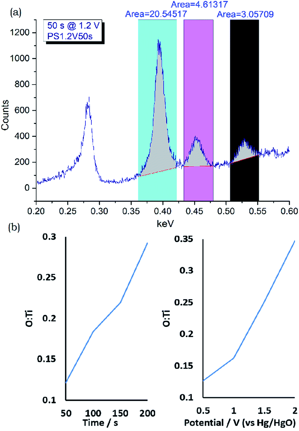 | ||
| Fig. 8 (a) Exemplar integrated WDX spectrum of a potential step oxidised TiN foil showing the regions used to analyse Ti + N, Ti and O content (top, full set of spectra in Fig. S22–S24†), (b) and the calculated O:Ti ratios compared with time at 1.2 V (bottom left) and potential at 100 s (bottom right). | ||
Discussion of capacitance vs. surface treatment
Table 3 shows some of the CV measured capacitance values for as-prepared and surface oxidised electrodes in the initial fast CV cycles at 1000 mV s−1, the subsequent slow cycles at 1 mV s−1 and the final fast cycles at 1000 mV s−1. In most cases no major increase in the capacitance is found in the initial cycles, and often there is a reduction. However, many of the surface oxidations, especially the electrochemical oxidations, result in a development of greater capacitance in the subsequent cycles.| Electrode treatment | Areal capacitance based on AFM surface area (or based on electrode geometric area)/μF cm−2 | ||
|---|---|---|---|
| Initial 1000 mV s−1 set, 5th scan | 1 mV s−1 set, 5th scan | Final 1000 mV s−1 set, 50th scan | |
| As prepared | 30.7 (215) | 915 (6410) | 35.1 (246) |
| TO 250 °C 24 h | 20.2 (97.0) | 200 (960) | 92.2 (443) |
| TO 350 °C 24 h | 9.07 (43.5) | 184 (883) | 15.5 (74.4) |
| PSO 0.5 V 100 s | 43.5 (222) | 709 (3620) | 61.2 (312) |
| PSO 1.0 V 100 s | 34.9 (178) | 305 (1560) | 83.1 (424) |
| PSO 1.2 V 150 s | 13.2 (67.3) | 2170 (11100) |
30.1 (154) |
| PSO 1.2 V 200 s | 19.9 (101) | 1990 (10100) |
56.1 (286) |
At low scan rate there is a greater opportunity to fully utilise any pseudocapacitance and it is noteworthy that the largest capacitance values are found in samples that have been potential step oxidised over the longest time periods. The areal capacitance values of these films based on geometric area of the electrode are comparable with the highest values we found in the literature (Table 4), by Achour et al.,13 which were measured on 2 μm thick porous films. The AFM evidence suggests that our films do not have significant porosity and the WDX shows they are likely to be much thinner.
| Form of TiN | Scan rate/mV s−1 | Geometric areal capacitance/μF cm−2 | Gravimetric capacitance/F g−1 | Sample areal capacitance/μF cm−2 |
|---|---|---|---|---|
| Nanocrystalline powder (128.7 m2 g−1)9 | 2 | — | 238 | 186 |
| 100 | — | 50 | 39 | |
| Nanocrystalline powder (26 m2 g−1)10 | Not given | — | 100 | 385 |
| “Nanocorn” structured films11 | 1000 | 2000 | — | — |
| Nanotube array12 | 5 | 3250 | — | — |
| 200 | 2500 | — | — | |
| Porous films13 | 2 | 18000 |
— | — |
| 100 | 8800 | — | — | |
| Ordered macroporous film (65.6 m2 g−1)14 | 2 | — | 266.8 | 407 |
In the final fast scans the highest areal capacitances were found in films that had been subjected to relatively gentle conditions and had thinner oxide films, and both thermal oxidation at 250 °C and potential step oxidation for 100 s at 1.0 V provided a 3-fold increase in capacitance compared with the as-prepared material at the same stage in cycling (Table 3). The areal capacitances drop off much more rapidly than those seen in porous and nanostructured thin films (Table 4) and this probably reflects a much larger proportion of the capacitance coming from the double layer and redox reactions within the top few layers of atoms. The better performance of porous films with good electronic connectivity to the surfaces at these faster scan rates suggests that a much larger proportion of their capacity is based on these mechanisms at all scan rates.
Comparing capacitance values with literature reports on nanocrystalline materials is difficult since these tend to be quoted as gravimetric specific capacitance. However, where surface areas are quoted it is possible to convert to an areal capacitance in order to make direct comparisons (Table 4). Our oxidised TiN foils outperform the values in the literature significantly at slow scan rate and the one example we found of a nanocrystalline material cycled at a relatively fast rate (39 F cm−2 at 100 mV s−1 by Choi et al.9) closely matches the areal capacity of our as-prepared material. Whilst our low surface area electrodes do not have sufficient capacitance for commercial supercapacitor applications, these results suggest that with high surface area materials there is sufficient scope to apply oxidative surface treatments before cycling in order to obtain higher capacities at all scan rates.
Conclusions
The surfaces of metal nitrides form oxide layers and reactions of these layers have been invoked to explain the redox component of their capacitance. Thermal oxidation of titanium nitride results in an increase in the amount of oxide on the surface, but this is not active in charge storage in aqueous KOH electrolyte. When very thin, this layer can develop over the duration of during electrochemical cycling into a material with an increased capacitive performance. Electrochemical oxidation of the surface at potentials positive of those typically used during cycling of titanium nitride produces thicker oxide layers that do increase the capacitance. This does not appear to be due to an increase in the surface area, which actually decreases, but to the production of an electrochemically active oxide surface. Again the capacitance then increases during normal potential cycling. Comparison of the achieved capacitances calculated as a function of the real surface area of the titanium nitride with those available in the literature suggests that higher capacitances could be achieved by applying such surface treatments to higher surface area electrode structures.Acknowledgements
The authors thank EPSRC for funding to BG (EP/P504740/1), and for funding the Smartlab diffractometer (EP/K00509X/1 and EP/K009877/1) and the EDX/WDX system (EP/I033394/1). XPS data were collected at the National Centre for Electron Spectroscopy and Surface Analysis (NCESS, Daresbury Laboratory). Thanks to Dr Matthew Roberts for assistance with the initial electrochemical measurements, and to Mrs Mahboba Hasan for collecting some of the XRD and SEM/WDX data.References
- J. R. Miller and A. F. Burke, Electrochem. Soc. Interface, 2008, 17, 53–57 CAS
.
- B. E. Conway and W. G. Pell, J. Solid State Electrochem., 2003, 7, 637–644 CrossRef CAS
- X. Zhao, B. M. Sánchez, P. J. Dobson and P. S. Grant, Nanoscale, 2011, 3, 839–855 RSC
- K. Naoi and P. Simon, Electrochem. Soc. Interface, 2008, 17, 34–37 CAS
- D. A. Mckeown, P. L. Hagans, L. P. L. Carette, A. E. Russell, K. E. Swider and D. R. Rolison, J. Phys. Chem. B, 1999, 103, 4825–4832 CrossRef CAS
- C. Hu, W. Chen and K. Chang, J. Electrochem. Soc., 2004, 151, A281–A290 CrossRef CAS
- C. C. Hu, K. H. Chang, M. C. Lin and Y. T. Wu, Nano Lett., 2006, 6, 2690–2695 CrossRef CAS PubMed
- C. F. Windisch, J. W. Virden, S. H. Elder, J. Liu and M. H. Engelhar, J. Electrochem. Soc., 1998, 145, 1211–1218 CrossRef CAS
- D. Choi and P. N. Kumta, J. Electrochem. Soc., 2006, 153, A2298–A2303 CrossRef CAS
- R. A. Janes, M. Aldissi and R. B. Kaner, Chem. Mater., 2003, 15, 4431–4435 CrossRef CAS
- P. Yang, D. Chao, C. Zhu, X. Xia, Y. Zhang, X. Wang, P. Sun, B. K. Tay, Z. X. Shen, W. Mai and H. J. Fan, Adv. Sci., 2015, 3, 1500299 CrossRef PubMed
- Y. Xie, Y. Wang and H. Du, Mater. Sci. Eng., B, 2013, 178, 1443–1451 CrossRef CAS
- A. Achour, R. L. Porto, M.-A. Soussou, M. Islam, M. Boujtita, K. A. Aissa, L. Le Brizoual, A. Djouadi and T. Brousse, J. Power Sources, 2015, 300, 525–532 CrossRef CAS
- D. J. Kim, J. K. Kim, J. H. Lee, H. H. Cho, Y.-S. Bae and J. H. Kim, J. Mater. Chem. A, 2016, 4, 12497–12503 CAS
- D. Choi, G. E. Blomgren and P. N. Kumta, Adv. Mater., 2006, 18, 1178–1182 CrossRef CAS
- D. Choi and P. N. Kumta, Electrochem. Solid-State Lett., 2005, 8, A418–A422 CrossRef CAS
- X. Zhou, H. Chen, D. Shu, C. He and J. Nan, J. Phys. Chem. Solids, 2009, 70, 495–500 CrossRef CAS
- P. J. Hanumantha, M. K. Datta, K. S. Kadakia, D. H. Hong, S. J. Chung, M. C. Tam, J. A. Poston, A. Manivannan and P. N. Kumta, J. Electrochem. Soc., 2013, 160, A2195–A2206 CrossRef CAS
- X. Lu, M. Yu, T. Zhai, G. Wang, S. Xie, T. Liu, C. Liang, Y. Tong and Y. Li, Nano Lett., 2013, 13, 2628–2633 CrossRef CAS PubMed
- R. Lucio-Porto, S. Bouhtiyya, J. F. Pierson, A. Morel, F. Capon, P. Boulet and T. Brousse, Electrochim. Acta, 2014, 141, 203–211 CrossRef CAS
- Z. Hou, K. Guo, H. Li and T. Zhai, CrystEngComm, 2016, 18, 3040–3047 RSC
- P. J. Hanumantha, M. K. Datta, K. Kadakia, C. Okoli, P. Patel and P. N. Kumta, Electrochim. Acta, 2016, 207, 37–47 CrossRef CAS
- D. Choi and P. N. Kumta, J. Am. Ceram. Soc., 2011, 94, 2371–2378 CrossRef CAS
- H. Cui, G. Zhu, X. Liu, F. Liu, Y. Xie, C. Yang, T. Lin, H. Gu and F. Huang, Adv. Sci., 2015, 2, 1500126 CrossRef PubMed
- S. I. U. Shah, A. L. Hector, X. Li and J. R. Owen, J. Mater. Chem. A, 2015, 3, 3612–3619 CAS
- C. Chen, D. Zhao and X. Wang, Mater. Chem. Phys., 2006, 97, 156–161 CrossRef CAS
- S. L. Roberson, D. Finello and R. F. Davis, J. Appl. Electrochem., 1999, 29, 75 CrossRef CAS
- T.-C. Liu, W. G. Pell, B. E. Conway and S. L. Roberson, J. Electrochem. Soc., 1998, 145, 1882–1888 CrossRef CAS
- S. I. U. Shah, A. L. Hector and J. R. Owen, J. Power Sources, 2014, 266, 456–463 CrossRef CAS
- S. Bouhtiyya, R. Lucio Porto, B. Laïk, P. Boulet, F. Capon, J. P. Pereira-Ramos, T. Brousse and J. F. Pierson, Scr. Mater., 2013, 68, 659–662 CrossRef CAS
- A.-R. Ko, S.-B. Han, Y.-W. Lee and K.-W. Park, Phys. Chem. Chem. Phys., 2011, 13, 12705–12707 RSC
- Y. Xie and X. Fang, Electrochim. Acta, 2014, 120, 273–283 CrossRef CAS
- M. Gnerlich, E. Pomerantseva, K. Gregorczyk, D. Ketchum, G. Rubloff and R. Ghodssi, J. Micromech. Microeng., 2013, 23, 114014 CrossRef
- S. Dong, X. Chen, L. Gu, X. Zhou, H. Wang, Z. Liu, P. Han, J. Yao, L. Wang, G. Cui and L. Chen, Mater. Res. Bull., 2011, 46, 835–839 CrossRef CAS
- F. Tian, Y. Xie, H. Du, Y. Zhou, C. Xia and W. Wang, RSC Adv., 2014, 4, 41856–41863 RSC
- Z. Wang, Z. Li and Z. Zou, J. Power Sources, 2015, 296, 53–63 CrossRef CAS
- C. Zhu, P. Yang, D. Chao, X. Wang, X. Zhang, S. Chen, B. K. Tay, H. Huang, H. Zhang, W. Mai and H. J. Fan, Adv. Mater., 2015, 27, 4566–4571 CrossRef CAS PubMed
- K. Grigoras, J. Keskinen, L. Grönberg, E. Yli-Rantala, S. Laakso, H. Välimäki, P. Kauranen, J. Ahopelto and M. Prunnila, Nano Energy, 2016, 26, 340–345 CrossRef CAS
- E. Kao, C. Yang, R. Warren, A. Kozinda and L. Lin, Sens. Actuators, A, 2016, 240, 160–166 CrossRef CAS
- P. K. Ajikumar, M. Kamruddin, R. Nithya, P. Shankar, S. Dash, A. K. Tyagi and B. Raj, Scr. Mater., 2004, 51, 361–366 CrossRef CAS
- B. H. Toby, J. Appl. Crystallogr., 2001, 34, 210–213 CrossRef CAS
-
A. C. Larson and R. B. Von Dreele, General structure analysis system (GSAS), Regents Univ. Calif., 1985, 748, LAUR, pp. 86–748 Search PubMed
- M. C. Biesinger, L. W. M. Lau, A. R. Gerson and R. S. C. Smart, Appl. Surf. Sci., 2010, 257, 887–898 CrossRef CAS
-
L. Meites, Handbook of Analytical Chemistry, McGraw-Hill Book Company, New York, 1963 Search PubMed
- “ZView computer Programme”, 2016, http://www.scribner.com
- B. L. Henke, E. M. Gullikson and J. C. Davis, At. Data Nucl. Data Tables, 1993, 54, 181 CrossRef CAS
- Inorg. Cryst. Struct. Database (ICSD, Fiz Karlsruhe) accessed via EPSRC-funded Natl. Chem. Database Serv. hosted by R. Soc. Chem.
- PDF-2 (Powder Diffr. File), 2012 release, Int. Cent. Diffr. Data, Swart. PA.
- N. C. Saha and H. G. Tompkins, J. Appl. Phys., 1992, 72, 3072–3079 CrossRef CAS
- C. Robertson, R. Beanland, S. A. Boden, A. L. Hector, R. J. Kashtiban, J. Sloan, D. C. Smith and A. Walcarius, Phys. Chem. Chem. Phys., 2015, 17, 4763–4770 RSC
-
P. Atkins, Elements of Physical Chemistry, Oxford, 5th edn, 2009 Search PubMed
- J. M. Elliott and J. R. Owen, Phys. Chem. Chem. Phys., 2000, 2, 5653–5659 RSC
-
K. F. J. Heinrich, Quantitative Electron Probe Microanalysis: Proceedings of a Seminar Held at the National Bureau of Standards, U.S. National Bureau of Standards, Gaithersburg, 1968 Search PubMed
- Tables Phys. Chem. Constants (16th Ed. 1995). 2.1.4 Hygrometry. Kaye Laby Online. Version 1.0 www.kayelaby.npl.co.uk.
Footnote |
| † Electronic supplementary information (ESI) available. See DOI: 10.1039/c6ta08308k |
| This journal is © The Royal Society of Chemistry 2017 |