
 Open Access Article
 This Open Access Article is licensed under a
 Creative Commons Attribution 3.0 Unported Licence
Mesoporous niobium-doped titanium dioxide films from the assembly of crystalline nanoparticles: study on the relationship between the band structure, conductivity and charge storage mechanism†
Junpei
Yue
a,
Christian
Suchomski
a,
Pascal
Voepel
a,
Ruediger
Ellinghaus
a,
Marcus
Rohnke
a,
Thomas
Leichtweiss
a,
Matthias T.
Elm
ab and
Bernd M.
Smarsly
*a
aInstitute of Physical Chemistry, Justus-Liebig-University Giessen, Heinrich-Buff-Ring 17, 35392 Giessen, Germany. E-mail: bernd.smarsly@phys.chemie.uni-giessen.de
bInstitute of Experimental Physics I, Justus-Liebig-University Giessen, Heinrich-Buff-Ring 16, 35392 Giessen, Germany
First published on 31st October 2016
Abstract
The charge storage mechanism of nanostructured intercalation materials such as anatase (TiO2) is still a matter of intense research, because it provides the basis for designing electrochemical energy storage and conversion materials. In this work, we addressed the relationship between conductivity and the charge storage mechanism exemplified with nanostructured Nb-doped TiO2. Nanoparticles of Nb-doped TiO2 were prepared by a novel two-step solvothermal process based on tert-amyl alcohol as the solvent. Several state-of-the-art techniques, including X-ray diffraction along with Rietveld refinement and Raman and X-ray photoelectron spectroscopy, were used to analyze the phase composition, the chemical oxidation state and the structure after doping with different niobium contents. Mesoporous Nb-doped TiO2 films with uniform pore sizes of 15 to 18 nm were produced by dip-coating employing these nanoparticles as building blocks. It is found that 5 at% Nb-doped TiO2 exhibits the highest conductivity. The analysis of the peak currents in the cyclic voltammetry of the mesoporous films indicates that the pseudocapacitive current contribution varies with the conductivity in the same trend. This correlation can be described qualitatively by the changes in the space charge layer at the interface with varying carrier concentration. Such a finding implies that doping not only affects the charge storage in the bulk due to changes of kinetic parameters including the chemical diffusion coefficient and electronic conductivity, but also influences the surface-related storage mechanism of a given nanostructured material. These results further provide a valuable insight in searching for and designing materials applied in pseudocapacitors.
1. Introduction
Titanium dioxide in the anatase structure has been widely studied as a promising anode material for both lithium-ion batteries and sodium-ion batteries.1–7 Recently, much attention has been paid to the charge storage mechanism.8–13 It is generally acknowledged that Li+ ions can reversibly be inserted into anatase inducing a structural phase transition accompanied with the formation of a lithium-poor tetragonal phase (Li0.05TiO2, SG I41/amd) and a lithium-rich orthorhombic phase (Li0.5TiO2, SG Imma).14 This transition is regarded as the main mechanism for the charge storage in anatase. As the crystallite size of anatase is decreased to less than 10 nm, the contribution of the interfacial faradaic processes to the charge storage of cations, known as the pseudocapacitive effect,15,16 significantly increases.12 In this context, Dunn et al. have reported that the pseudocapacitive contribution can reach up to 55% for the crystallite size of 7 nm.12As summarized in Fig. 1, different mechanisms of electrochemical charge storage are discussed to be relevant in nanosized metal oxides: aside from the intercalation process, different surface-related storage mechanisms have to be distinguished, which contribute to capacitive charge storage, namely faradaic (“pseudocapacitive”) and non-faradaic (“double layer capacitive”) effects. The pseudocapacitive charge storage is a matter of high importance and the study has been conducted on many intercalation materials such as Nb2O5, MoO3, and TiS2.17–20 Brezesinski et al. compared the pseudocapacitive charge storage of anatase-based electrodes possessing different nanostructured morphologies, including ordered porous and nonporous films prepared by dip-coating of TiO2 nanoparticles and molecular TiO2 precursors as building blocks along with amphiphilic block copolymers as structuring agents.10 The obtained results indicated that a high specific surface area in combination with mesoporosity significantly enhances the pseudocapacitive contribution.10 In particular, the investigators evidenced that a mesoporous thin film based on preformed nanoparticles presents an advantageous morphology in order to study the pseudocapacitive effect and the influence of surfaces on electrochemical charge storage in general.21 Additionally, Augustyn et al. studied the importance of crystallinity on the pseudocapacitive behaviour of Nb2O5, showing that the pseudocapacitive charge storage of Li+ ions preferentially occurs in the crystalline phase.22 In the past ten years, numerous parameters, including size effects, morphology effects and crystallinity on pseudocapacity have been studied in detail.
 | ||
| Fig. 1 Different mechanisms of electrochemical charge storage in nanosized metal oxides. | ||
In spite of such recent achievements, certain important issues have not been understood until now. Major goals are the elucidation of the difference between interfacial charge storage and bulk reactions and finally to optimize the two parts for practical applications. The work of Shin et al. showed that an increase in the Li rate capability can be accomplished by endowing TiO2 with a higher intrinsic conductivity, which was achieved by partial reduction with H2.3 Investigators have proved that the rate capacity can be enhanced by increasing the conductivity from the kinetic standpoint. For nanomaterials, such studies thus pointed to the importance of understanding the relationship between conductivity and pseudocapacity, which represents the main topic of our study. As reported previously, the pseudocapacitive charge storage is related to the electrochemical potential of Li, which is dependent on the grain size or the surface structure of active materials.16 Therefore the pseudocapacitive charge storage significantly increases for materials with small grain size and high crystallinity.16 The correlation between conductivity and (pseudocapacitive) charge storage is of substantial fundamental importance, addressing the interplay between a thermodynamic process on the surface (electrochemical potential of Li) and charge transport (conductivity). In essence, by experimentally determining the relationship between the conductivity on charge storage parameters, valuable insights into pseudocapacitive charge storage can be expected.
To address this important issue, in the present study Nb-doped TiO2 (Nb:TiO2) was employed to study the impact of conductivity on pseudocapacitive charge storage. As reported previously, the conductivity of Nb:TiO2 can be tuned by different doping concentrations, while the intercalation reaction remains unaltered.4,5,23 As mentioned above, mesoporous films possess a suitable morphology for the investigation of interfacial charge storage, as the connected pores can alleviate the concentration polarization process to some extent by providing a mass transport path and an easy access to surface redox sites.21,24,25 Wang et al. reported the synthesis of mesoporous Nb:TiO2 based on a sol–gel approach.4 However, the relatively small specific surface area, the imprecisely controlled crystallinity and crystallite size are main drawbacks for constructing mesoporous films by this procedure.2,10,26 Fortunately, colloidal nanoparticles offer a suitable alternative to the mentioned sol–gel method. De Trizio et al. reported colloidal Nb:TiO2 nanoparticles and Milliron et al. proved the occurrence of capacitive charge storage in these nanoparticles using spectroelectrochemical signatures.27,28 Darr et al. reported Nb:TiO2 with an Nb content of 25 at% by using a continuous hydrothermal flow synthesis reactor using a supercritical water flow as a reagent, and the pseudocapacitive charge storage in the nanoparticles takes up by 65%.13 Yet, these nanoparticles can hardly be utilized as building blocks for generating self-assembled nanostructures by templating liquid-crystalline mesophases due to their poor dispersibility in required solvents, e.g. alcohols. Bein et al. reported on Nb:TiO2 nanoparticles and mesoporous films from preformed nanoparticles; however, this study shows that an alteration in the mesoporosity is induced for different Nb contents, thus aggravating the distinction of the respective impact of mesoporosity and Nb doping.29
One task of the present study is to develop a tailor-made preparation approach of Nb:TiO2 nanoparticles possessing designed Nb contents. In order to correlate the electrochemical properties (pseudocapacitive storage mechanism) with the composition as well as the conductivity, the requirement was the preparation of Nb:TiO2 films with different compositions, yet with similar mesoporous morphologies and crystallite sizes. By such a procedure, the relationship between conductivity and surface charge storage can be addressed.
Here, an optimized solvothermal protocol was developed to prepare colloidal Nb:TiO2 nanoparticles with an average diameter of 7 nm based on our previously described synthetic route.11 A microwave reactor was used because this technique allows both rapid and uniform heating.30,31 The procedure applied in the present study allows for a completion of the reaction within 6 minutes. The as-prepared nanoparticles possess high crystallinity and good dispersibility in polar solvents (e.g. 10 wt% in water or 5 wt% in ethanol) without further post-functionalization. Several state-of-the-art techniques including XRD, XPS and spectroscopic methods were used to investigate the phase composition as well as the electronic properties of these Nb:TiO2 nanoparticles. Ordered mesoporous films were prepared by an evaporation-induced self-assembly process, using the diblock copolymer poly(iso-butylene)-block-poly(ethylene oxide) (PIB45-b-PEO50) as the structure-directing agent and crystalline Nb:TiO2 nanoparticles. The beneficial templating properties of this class of block copolymers were reported previously.32–35 The electrochemical performance and pseudocapacitive effect of such films were studied by galvanostatic profiles, cyclic voltammetry and impedance analysis.
2. Experimental
Materials
Titanium(IV) chloride (99.0%), titanium(IV) ethoxide (97%), niobium(V) ethoxide (99.95%), 2-methoxyethanol (99.8%), lithium perchlorate (99.9%), lithium ribbon (99.9%) and anhydrous propylene carbonate (99.7%) were purchased from Sigma Aldrich. 1-Hexanol, tert-amyl alcohol were purchased from abcr GmbH, while ethanol, n-pentane and diethyl ether were purchased from VWR. Indium tin oxide (ITO) coated glass slides and optical glasses were purchased from Glaswerke Haller GmbH and VWR, respectively. The copolymer PIB50-b-PEO45 was obtained from BASF.Synthesis of Nb:TiO2 nanoparticles
In a representative synthesis, 0.25 mL of TiCl4, 0.5 mL of Ti(OEt)4 and the corresponding amount of Nb(OEt)5 were added to a 30 mL glass vial and then subjected to microwave irradiation with the temperature of 75 °C and the time of 1 min. Followed by the addition of 12 mL of 1-hexanol into the above precursor solution, the mixture solution was treated at 110 °C for 1 min. Afterwards 8 mL of tert-amyl alcohol were introduced to the mixture solution, followed by rapid heating to 140 °C and holding for 5 min. In order to obtain similar crystallite sizes, the reaction time for the doped products was 6 min. After quenching to 55 °C, the nanoparticles were precipitated from the primitive solution by adding n-pentane and then washed with diethyl ether three times. The obtained nanoparticles were dried at room temperature for 12 hours. In order to remove the organic residue, the as-made nanoparticles were subjected to 400 °C for one hour.Preparation of Nb:TiO2 films
In typical dip-coating experiments, 60 mg of the as-made nanoparticles and 40 mg of PIB50-b-PEO45 were dissolved in 1.5 mL of ethanol and 0.5 mL of 2-methoxyethanol, respectively. Then the polymer solution was added into the nanoparticle dispersion drop by drop. After stirring for half an hour, the transparent dip-coating solution was obtained. Thin films were prepared by dip-coating on different substrates (silicon wafers, ITO glass, and optical glass) at a relative humidity of 80% and a withdrawing rate of 10 mm s−1. The film was stabilized for 5–10 min in the dip-coating chamber and then transferred into the oven preheated at 120 °C. After one hour the temperature was increased up to 300 °C at a ramp of 1 °C min−1 and was then maintained for 6 hours. The polymers could be removed by heat-treatment to 400 °C (a ramp of 10 °C min−1).Characterization methods
The microwave-assisted reaction was carried out on a Monowave 300 microwave reactor from Anton Paar Germany. Dynamic light scattering (DLS) data were collected in 1 wt% dispersions in water on a Zetasizer Nano from Malvern. Thermal gravimetric analysis (TGA) data were obtained with a Netzsch STA 409 PC. Bright-field transmission electron microscopy (TEM) images were acquired using a CM30-ST microscope from Philips. Wide-angle X-ray diffraction (WAXD) measurements were carried out using an X'Pert PRO diffractometer from PANalytical instruments. Rietveld refinement was performed with the FullProf software using the 6 coefficient polynomial background and Thompson–Cox-pseudo-Voigt peak function. The grain size was calculated via an anisotropic Lorentzian size broadening approach. Unpolarized Raman spectra were collected on the SENTERRA dispersive Raman spectrometer from Bruker Optics equipped with an objective from Olympus (MPlan N 100×; field number 22 and a numerical aperture of 0.9) and a Nd:YAG laser (λ = 532 nm and P = 2 mW). X-ray photoelectron spectroscopy (XPS) spectra were acquired on a PHI VersaProbe Scanning ESCA Microprobe (Physical Electronics) with a monochromatic Al Kα X-ray source. The C 1s signal from adventitious hydrocarbon at 284.8 eV was used as the energy reference to calibrate charging effects. Nitrogen physisorption measurements were conducted at 77 K on an Autosorb-6-MP automated gas adsorption station from Quantachrome Instruments. Optical absorption measurements were carried out on a Perkin-Elmer Lambda 750 UV-Vis-NIR spectrophotometer equipped with a Praying-Mantis diffuse reflectance attachment. Spectralon type DRP-SPR from Harrick Scientific Products was used as a reflectance standard. The collected diffuse reflectance spectra were converted into absorption spectra according to the Kubelka–Munk function F(R) = (1 − R)2/2R, where F(R) is the Kubelka–Munk function and R is the diffuse reflectance of the sample for “infinite” thickness relative to the reflectivity of the white standard. Scanning electron microscopy (SEM) micrographs were taken with a MERLIN instrument from Carl Zeiss. For SIMS depth profiling a ToF-SIMS 5-100 instrument (IonTof GmbH, Münster, Germany) was used. The primary ion gun was operated in high-current-bunched mode, with 25 keV Bi+ ions as primary ion species. Sputtering was done with 1 keV O2+ ions. The analysis area was 100 × 100 μm2 in the center of a 220 × 220 μm2 sputter area. For charge compensation a low energy electron flood gun was used and the analysis was performed in non-interlaced mode with a 1.5 s pause time. For depth calibration the sputter crater depths were measured using a profiler (Alpha step IQ, KLA-tencor). The obtained mass resolution was m/Δm > 9100 for Nb+.Conductivity measurements
The conductivity measurements were carried out on mesoporous thin films (a thickness of approximately 200 nm) on glass substrates by potentiostatic impedance spectroscopy. As current collectors two parallel indium layers were used with a thickness of 200 nm and an area of 5 × 5 mm. The distance of the two parallel electrodes was 1 mm. The schematic of the setup is shown in Fig. S7.† The impedance spectra were recorded on the SP-300 potentiostat from BioLogic in the frequency range from 7 MHz to 0.01 Hz. The voltage amplitude was 60 mV.Electrochemical measurements
The electrochemical measurements were conducted in a glovebox with pO2 ≤ 0.5 ppm and pH2O ≤ 0.5 ppm, with lithium foil and wire as the counter electrode and reference electrode, and mesoporous Nb:TiO2 films on ITO substrates as the working electrode. 1 mol L−1 LiClO4 in propylene carbonate solution was used as the electrolyte. The potential was controlled by using an Autolab Potentiostat with 1.4 and 2.5 V as the cut-off potentials for the cyclic voltammetry (CV) and galvanostatic discharge/charge profiles, respectively. The scanning rates for CVs were adjusted to 0.2, 0.5, 1, 2 and 5 mV s−1.3. Results and discussion
Nb:TiO2 nanoparticles were prepared by a microwave-assisted solvothermal route. Compared with the method introduced by Bein et al.,29tert-amyl alcohol was used as the solvent and the primary alcohol 1-hexanol was used to control the condensation reactions and improve the dispersibility. Furthermore, the combination of these two alcohols was developed in order to control the particle size: when using 1-hexanol as a co-solvent, the ethoxy groups in TiCl2(OEt)2 are replaced by hexyloxy groups due to the ligand exchange at elevated temperatures.36 As a consequence, the introduced hexyloxy moiety slows down the reaction rate of the condensing Ti–Cl and Ti–OR groups which produces larger nanoparticles. In the final products, the residual primary alkoxy groups help to redisperse the nanoparticles in alcohols, which in turn facilitates the block-copolymer templating. Thus, the usage of 1-hexanol exerts a major impact on the sol–gel mechanism and thus represents a crucial advance in the synthesis of such nanoparticles in general.The as-prepared nanoparticles have good dispersibility in water (≥10 wt%) and ethanol (up to 5 wt%). Representative photographs of dispersions with a concentration of 10 wt% are shown in Fig. 2. The DLS measurements show the average (hydrodynamic) particle sizes of 5.6, 6.5 and 7.5 nm for 2 at%, 5 at% and 10 at% Nb:TiO2, respectively. The nanoparticles are positively charged with the zeta potentials being +(40 ± 20) mV. The obtained hydrodynamic diameters are comparable with the crystallite sizes determined from XRD measurements on the as-prepared nanoparticles (see Fig. S1†), implying the absence of aggregation in water. The reason for good dispersibility will be elaborated later. The thermogravimetric analysis with recording mass spectrometry (TGA-MS) of the as-prepared particles (shown in Fig. S1†) indicates that organic residues take up to 8 wt% and can be removed by a heat-treatment in air by 400 °C. The following characterization was carried out on nanoparticles annealed at 400 °C for one hour.
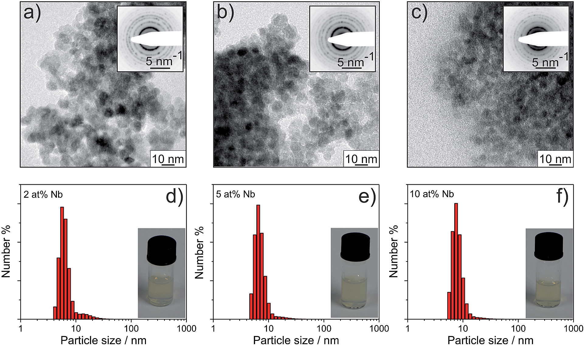 | ||
| Fig. 2 TEM images and DLS data of the as-prepared Nb:TiO2 nanoparticles with different doping levels: 2 at% (a and d); 5 at% (b and e) and 10 at% (c and f). The inset images show SAED patterns as well as photographs of particle dispersions (10 wt% solid) in water, respectively. | ||
Nb:TiO2 nanoparticles were investigated by transmission electron microscopy (TEM) and the results are shown in Fig. 2. Based on TEM images, the nanoparticles present a spherical shape, and the average particle sizes for 2 at%, 5 at% and 10 at% Nb:TiO2 are 8.0 ± 0.5 nm, 7.5 ± 0.5 nm and 6.0 ± 0.5 nm, respectively. With increasing doping levels, the particle size thus decreases by ca. 2 nm. Lattice planes can be clearly observed in TEM analysis, which confirms the high crystallinity. The electron diffraction patterns (Fig. S2†) can be assigned to the (101), (004), (200), (105) or (211) and (204) crystalline planes of the anatase phase according to JCPDS card no. 21-1272. The distinct electron diffraction signals further prove the well-developed crystallinity of these Nb:TiO2 particles.
Microstructure of Nb:TiO2 nanoparticles
XRD patterns along with Rietveld refinement and Raman spectra were used to further analyze the phase composition of Nb:TiO2 nanoparticles and the results are shown in Fig. 3 and S3.† All XRD patterns present the characteristic anatase phase (SG I41/amd) according to the JCPDS card no. 21-1272 and were further analyzed by Rietveld refinement using the FullProf software. The values of chi2 are 1.75, 1.55, 2.08 and 3.21 for TiO2, 2 at%, 5 at% and 10 at% Nb:TiO2 patterns, respectively, speaking for a reasonable refinement. The unit cell parameters a, b and c linearly increase with the increase of Nb-doping levels (see Fig. 3b) and the unit cell volume increases from 136.59 to 137.53 Å3, which is in fair agreement with the literature report (shown in Table S1†).7,37 The increase in unit cell parameters is caused by the substitution of Ti4+ (octahedral site, 74.5 pm) by the larger Nb5+ (78 pm) ions, meanwhile such increase can be compensated somehow by the vacancies of Ti4+ and the release of oxygen. In combination of these two effects, the unit cell volume slightly increases after doping. The linear relationship suggests a homogeneous distribution of Nb5+ in the anatase structure for all doping levels. From the Rietveld refinement, the determined crystallite sizes are 6.4 ± 0.2, 6.3 ± 0.3, 6.5 ± 0.2, and 5.5 ± 0.2 nm. Thus, the uniformity in the crystallite sizes is quite beneficial for the interpretation of electrochemical properties, as this parameter can be ruled out as causing possible effects on the electrochemical performance. | ||
| Fig. 3 Characterization of Nb-doped TiO2 nanoparticles after heat-treatment at 400 °C for 1 hour. (a) XRD patterns of samples with different doping levels. (b) Unit cell parameters as a function of Nb content. (c) Rietveld refined XRD pattern of 5 at% Nb:TiO2. The orange crosses represent the fitting curve, the dark yellow curve is the difference between the observed and the calculated curve, and the purple bars stand for the peak position. (d) Raman spectra of Nb:TiO2 nanoparticles with different Nb contents. The inset shows the frequency region between 100 and 200 cm−1. Black, red, blue and magenta curves represent undoped, 2 at%, 5 at% and 10 at% Nb:TiO2, respectively. | ||
Raman spectra of Nb:TiO2 samples are shown in Fig. 3d. The Raman bands at 146, 197, 394, 516 and 641 cm−1 are in good agreement with the characteristic vibration modes of anatase (Eg, E1g, B1g, A1g and B1g, and Eg) according to the literature.38–40 No vibration bands from other TiO2 phases are observed, indicating phase-pure materials. With increasing the Nb-doping level, the first Eg band shifts to higher energy, while the B1g band shifts to lower wavenumbers. These changes are caused by the non-stoichiometry (vacancies of Ti4+ after Nb5+ doping) and the formation of Nb–O–Ti bonds.27,41 In the Raman spectroscopy of 10 at% Nb:TiO2, the broad, weak scattering band marked by an asterisk at ∼850 cm−1 is attributed to the vibration mode of the terminal Nb![[double bond, length as m-dash]](https://www.rsc.org/images/entities/char_e001.gif) O bond, corresponding to the network termination in NbOx.27,37,42 In conclusion, both the XRD data and Raman spectra prove the successful and homogeneous incorporation of Nb into the anatase lattice.
O bond, corresponding to the network termination in NbOx.27,37,42 In conclusion, both the XRD data and Raman spectra prove the successful and homogeneous incorporation of Nb into the anatase lattice.
To gain more insight into the (surface) composition and chemical oxidation state of the Nb:TiO2 nanoparticles, XPS measurements were carried out and the results are shown in Fig. 4 and S4.† From the survey spectra of Nb:TiO2 (Fig. S4†), only Ti, Nb, O, C and Cl signals are found. The latter can be comprehended as a residual ligand, which remains in very small quantities on the particle surface. The Cl ligands hydrolyze rapidly in water leading to positively charged particles with positive zeta potentials. This fact helps to explain why the nanoparticles have good dispersibility in water-containing organic solvents. The Nb contents for Nb:TiO2 nanoparticles with nominal doping levels of 2 at%, 5 at% and 10 at%, obtained by XPS analysis, are 2.3 at%, 4.9 at% and 9.7 at%, respectively. Within the accuracy of the detection limit, the Nb content found in the products is virtually identical to the used precursor ratio, confirming that the synthesis protocol was successful.
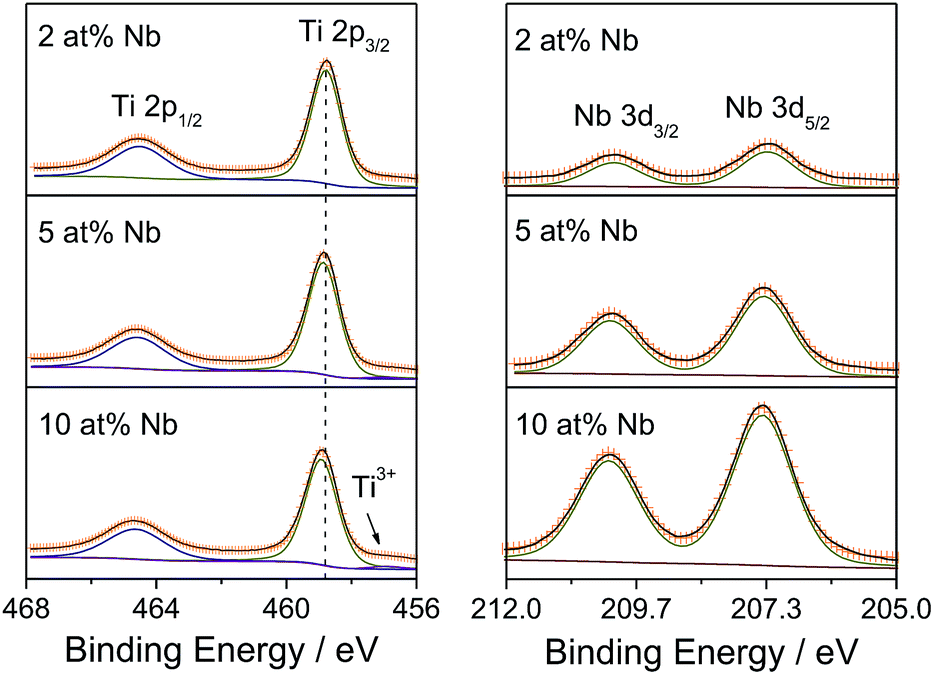 | ||
| Fig. 4 XPS scans of Ti 2p and Nb 3d core levels of Nb:TiO2 nanoparticles. The Shirley model was used to determine the background. The orange crosses represent the sum of the fittings and the black solid curves are the experimental data. | ||
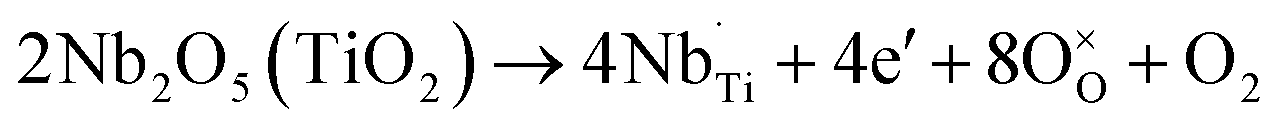
High-resolution XPS scans of the Ti 2p and Nb 3d core levels are shown in Fig. 4. The Ti 2p spectrum of 2 at% Nb:TiO2 exhibits an asymmetric doublet peak resulting from spin–orbit splitting with a binding energy of 458.8 eV for 2p3/2 and a splitting energy of 5.7 eV, in line with reported findings from previous studies.23 The binding energy for 2p3/2 slightly increases with increasing Nb content, which originates from the change of chemical environment after doping. Moreover, minor amounts of Ti3+ are observed in samples featuring high Nb proportions, evidenced by an additional peak at approximately 456.9 eV.43,44 Generally speaking, the charge compensation of Nb5+ substituting Ti4+ can be achieved by two mechanisms as shown in (1) and (2): one explanation is the reduction of 1 Ti4+ to 1 Ti3+ for every incorporated Nb5+ ion;29 the other possibility is the formation of 1 Ti vacancy per 4 Nb5+ ions introduced.42,45,48
 | (1) |
 | (2) |
Based on the XPS data, it can be concluded that at lower Nb5+ concentrations the charge compensation is likely compensated by the generation of Ti vacancies, while free electrons are possibly created at higher Nb contents. Moreover, all the Nb 3d spectra show symmetric spin–orbit doublets with Nb 3d5/2 binding energies of approximately 207.4 eV and splitting energies of 2.8 eV, indicating that niobium is only present in the +5 state.45–47 Lastly, the C 1s core level spectra can be deconvoluted into three peaks (see Fig. S4†) with binding energies of 284.8 eV, 286.2 eV and 288.9 eV, attributable to C–H/C–C, C–O and O–CO species,35 respectively, in accordance with the results by TGA-MS, as depicted in Fig. S1.†
Apart from the chemical composition, the optical properties were also investigated by UV-Vis-NIR absorbance spectroscopy and the results are shown in Fig. S3.† As seen, there is no significant absorption in the visible and near infrared region, indicating that all samples are practically transparent in this frequency range. The optical band gap (Eg) was obtained by the plot of (F(R) × hν)nvs. hν (photon energy), in which n = 1/2 and n = 2 represents an indirect or direct allowed optical transition, respectively. The analysis indicates indirect band gaps of (3.16 ± 0.01) eV for all samples, which demonstrate that Nb-doping has no significant impact on the band gap, as also reported in previous studies.46,49
Mesoporous Nb:TiO2 films
In order to obtain reliable information on the metal ion distribution in the mesoporous Nb:TiO2 thin films, a depth profile analysis by time-of-flight secondary ion mass spectrometry (ToF-SIMS) was performed on a ∼150 nm thick PIB45-b-PEO50-templated Nb:TiO2 thin film (10 at% Nb) heated to 400 °C. The advantage of using SIMS is its excellent sensitivity to niobium, which allows us to investigate its spatial distribution within the thin film structure. The ToF-SIMS profile in Fig. 5 shows the distribution of 48Ti+, 93Nb+ and 12C+ as a function of the depth from the top surface. It can be seen that both Ti and Nb ions are uniformly distributed throughout the bulk of the film without substantial deviations. Close to the film/substrate interface, the 93Nb+ SIMS signal increases slightly due to a small enrichment of Nb within this region, which is induced by a change in the ionization potential. Moreover, it can be inferred that the organic ligands (e.g., hexyloxy and ethoxy groups) are completely combusted at 400 °C from the 12C signal, in accordance with the findings by TGA-MS (Fig. S1†). To conclude, the ToF-SIMS data indicate no major fluctuations in the chemical composition and qualitatively agree with both the XPS and TG-MS results.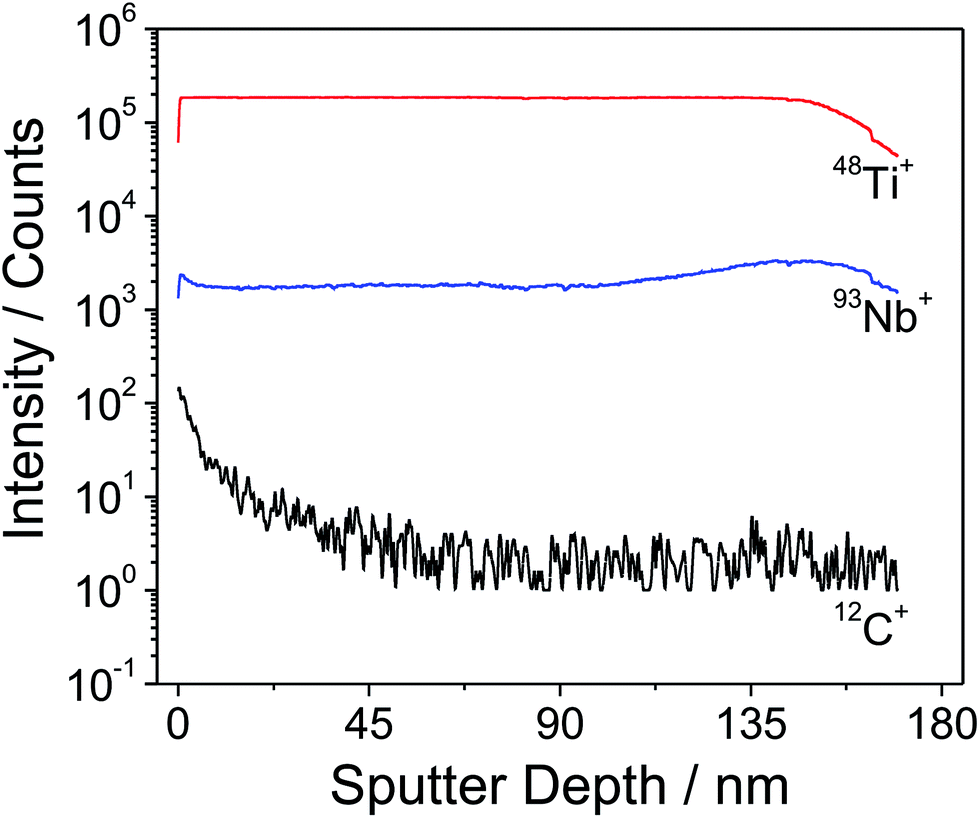 | ||
| Fig. 5 ToF-SIMS depth profile of an approximately 150 nm thick PIB45-b-PEO50-templated 10 at% Nb:TiO2 film after heating to 400 °C (10 °C min−1) showing the distribution of 48Ti+ (red), 93Nb+ (blue) and 12C+ (black). | ||
The mesoporous morphology of Nb:TiO2 thin films made by polymer templating using the diblock copolymer PIB45-b-PEO50 is shown in Fig. 6 and S5.† SEM reveals that the mesoporous films of the templated nanoparticles exhibit a uniform mesostructure with spherical pores and short- and long-range ordering, being in agreement with previous studies using this type of block copolymer.34–36 The pore diameter possesses a narrow distribution of 15 to 18 nm, as determined by analysis of ca. 100 mesopores. The wall thickness is located in the range of 6 to 8 nm, thus corresponding well to the average size of the Nb:TiO2 nanoparticles, indicating the successful co-assembly of nanoparticles and micelles. As explained above the nanoparticles are positively charged, thereby exhibiting an attractive interaction with the polar PEO chains of the PIB45-b-PEO50 block copolymer. This attraction probably facilitates the formation of such an ordered mesostructure. From cross-sectional SEM images, a continuously connected porous network can be observed spanning the films from the bottom to the top. It is seen that the thickness of the films is around 150–200 nm, which can be tuned by the withdrawal speed. The shape of mesopores in the view of the cross-sectional direction is ellipsoidal due to distortions and stress during solvent evaporation and heat-treatment. From the cross-sectional images, the mesopores are found to be 6 to 10 nm in height and 14 to 18 nm in length.
 | ||
| Fig. 6 Morphology of mesoporous PIB45-b-PEO50–templated Nb:TiO2 thin films after heating to 400 °C. (a–d) Top-view and cross-sectional SEM images of pure TiO2, 2 at%, 5 at% and 10 at% Nb:TiO2 films, respectively. | ||
In addition to SEM analysis, the mesoporosity of these films was analyzed in detail via N2 physisorption at 77 K. The adsorption/desorption isotherm in Fig. 7 exhibits a typical type-IV shape and a H1-type hysteresis, indicating spherical or cylindrical pores.50 However, the adsorption and desorption branches fall on top of each other at a small partial pressure (p/p0ca. 0.1). Such a phenomenon is typical for small amounts of the material, but inevitable in the light of the small amount of the material constituting a film. Here the N2 physisorption measurement was carried out on a mesoporous film with an area of 42 cm2 and a thickness of 600 ± 50 nm (in volume: 2.52 × 10⁻³ cm3). A hybrid nonlocal density functional theory (NLDFT) model was applied to the adsorption branch based on spherical/cylindrical pores for the calculation of the pore size distribution.51,52 This analysis provides an average pore diameter of ca. 10 nm, which is in agreement with the SEM results. The wide pore size distribution is caused by the distortion of the pore shapes, while the NLDFT model assumes a uniform shape. The absolute adsorbed pore volume on such a film is 1.4 × 10⁻³ cm3 and the calculated porosity is around 55%. According to the density of TiO2 (3.89 g cm−3), the estimated mass of TiO2 on the film is around 4.4 ± 0.4 mg and the specific mass is 1.75 g cm−3, which is used to estimate the mass for determining the specific capacity. The BET surface area for such a film is around 0.734 m2. The specific surface area is 291 m2 cm−3 and this value is used to estimate the real surface area of the electrodes applied in electrochemical measurements.
 | ||
| Fig. 7 (a) N2 adsorption and desorption isotherms of mesoporous TiO2 films possessing an area of 42 cm2 and thicknesses of (600 ± 50) nm. The pore size distribution was obtained by the NLDFT method based on a spherical/cylindrical pore model, using the data of the adsorption branch. (b) Impedance spectra of mesoporous doped TiO2 films. | ||
The total conductivity of the mesoporous Nb:TiO2 films has been investigated by two-electrode impedance spectra. Two parallel electrodes were used to measure the in-plane conductivity of mesoporous films on an insulating substrate (here glass was the substrate).53 The results are shown in Fig. 7 and present one semicircle corresponding to the overall resistance. The calculated conductivities are 1 × 10⁻⁵, 7.8 × 10⁻⁵, 9.8 × 10⁻⁵ and 7.9 × 10⁻⁵ S cm−1 for TiO2, 2 at%, 5 at% and 10 at% Nb:TiO2, respectively, i.e. doping with Nb increases the electrical conductivity by almost a factor of 10. As discussed by Furubayashi et al. the Nb doping of TiO2 thin films results in the formation of an impurity band near the bottom of the conduction band even at low doping concentrations (x < 1%) and thus in a dominant electronic conductivity.23 With increasing Nb content an increase of the electronic carrier concentration was reported, however, at higher doping levels (x > 6%) the ionization efficiency decreased again accompanied by a decrease of the mobility resulting in a maximum conductivity value at a doping level of about 6%.23 In nanocrystalline TiO2, additional extended band states below the conduction band minimum arise, where hopping of the electrons occurs.54,55 However, as for thin films Nb doping shifts the Fermi-energy closer to the conduction band edge improving the electronic conductivity.42,54 The same behavior is observed for our Nb:TiO2 mesoporous thin films where a maximum in electrical conductivity is found at a doping level of about 5 at%. At higher doping levels the mesoporous Nb:TiO2 thin films also seem to exhibit a reduction of the ionization efficiency due to trapping of electrons at Ti4+ as indicated by the XPS results, which hint for a small Ti3+ content for the 5 at% Nb:TiO2 and 10 at% Nb:TiO2 samples.46
In general, it is important to take into account the role of the processing on the electrochemical properties of Nb:TiO2 films. The conductivities of our Nb:TiO2 mesoporous films are comparable to values reported for nanostructured films,29 but lower than for films with similar Nb content prepared by pulsed laser deposition (PLD) or chemical vapor deposition (CVD).25,44 It is worth noting that the conductivities were calculated from the measured resistance assuming a dense thin film, i.e. the conductivities are underestimated as the mesoporous structure of our thin films was neglected. Thus, the values obtained can be considered only as a lower limit of the material's conductivity. Nevertheless, also the high density of grain boundaries between the single nanocrystallites may be responsible for a lower conductivity compared to that of the dense thin films prepared by PLD or CVD. Furthermore, as mentioned in the XPS part, the compensation mechanism may change depending on the oxygen partial pressure during the preparation or processing, which also affects the conductivity.
Pseudocapacitive behavior of mesoporous Nb:TiO2 films
The galvanostatic charge/discharge profiles and rate capacities of mesoporous 5 at% Nb:TiO2 films are shown in Fig. 8. The first cycle shows poor coulombic efficiency, which could be due to SEI formation and trapping of Li+ in irreversible sites.5 The specific capacity and coulombic efficiency become stable after five cycles. The discharge and charge plateaus after five cycles are 1.77 and 1.90 V, respectively, which are in good agreement with Li+ intercalation and extraction into anatase TiO2. The plateau corresponds to a two-phase equilibrium process between a lithium-poor phase of Li0.05TiO2 and a lithium-rich phase of Li0.5TiO2, contributing a specific capacity of around 90 mA h g−1. A gradient curve is followed by the plateau, which is normally assigned to the interfacial charge storage. Although it is hard to accurately evaluate the pseudocapacitive contribution by the gradient curve, it can be estimated to take up 47% of the specific capacity. The mesoporous thin film presents a reasonable rate performance as well. At a discharge and charge rate of 20C, the specific capacity is around 120 mA h g−1, exceeding the results reported in the literature.4 This result can possibly be caused by the improved dynamics for both electron transfer in doped-TiO2 nanoparticles and Li+ ion transport in connected mesopores.3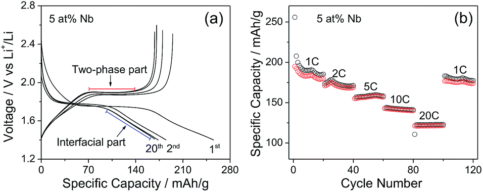 | ||
| Fig. 8 Discharge and charge profiles (a) and rate capacity performance (b) of 5 at% Nb:TiO2 mesoporous films. 1C means a discharge and charge current of 175 mA g−1. | ||
Scanning rate dependent cyclic voltammetry (CV) was recognized as the most efficient and widely used method to quantify the pseudocapacitive charge storage. The basic principle is based on the procedure of dividing the total stored charges into two parts (as shown in Fig. 1), namely one part resulting from a bulk reaction, which is a diffusion controlled intercalation reaction; the other part is assumed to be caused by surface reactions, which can be attributed to electrochemical double layer and redox reactions at the interface (hereafter the capacitance from the electrochemical double layer is neglected). The relationship between the current density and the scanning rate in CV can be described by
| j = aνb | (3) |
log![[thin space (1/6-em)]](https://www.rsc.org/images/entities/char_2009.gif) j = blogν + loga j = blogν + loga | (4) |
The current density of the insertion reaction is proportional to the square root of the scanning rates (b = 0.5), while the current density of the capacitive contribution is proportional to the scanning rates (b = 1). The equation can be further written as:
| jV = kCν + kFν1/2 | (5) |
Dividing by ν1/2 gives
| jV/ν1/2 = kCν1/2 + kF | (6) |
| kC = AC |
| kF = 0.4958nFAc(DLiαnF/RT)1/2 | (7) |
The cyclic voltammetric (CV) data of mesoporous 5% Nb:TiO2 are shown in Fig. 9 as a function of the scanning rate, while CV data for the other samples are included in Fig. S6.† The CV curves present a superposition of obvious redox signals and a capacitive contribution.57 The current maxima shift to higher potentials for the anodic signal and to lower potentials for the cathodic signal with increasing scanning rates, implying an irreversible electrochemical reaction system. A linear relationship between log(jpeak) and log(ν) is observed for the mesoporous Nb:TiO2 films (Fig. 9b), and the slopes (parameter b) for TiO2, 2 at%, 5 at% and 10 at% Nb:TiO2 are 0.63, 0.71, 0.72 and 0.70, respectively. Furthermore, a linear relationship between jpeak/ν1/2 and ν1/2 is observed for all films (Fig. 9c), allowing for a quantification of the pseudocapacitive current according to eqn (6) based on peak currents. The pseudocapacitive contribution will increase with increasing scan rates according to eqn (5) and (6), as shown by the data in Fig. S6.† The analysis provides the relative pseudocapacitive contributions from the cathodic process at a scanning rate of 1 mV s−1, which are 25%, 40%, 44% and 37% for TiO2, 2 at%, 5 at% and 10 at% Nb:TiO2, respectively. The pseudocapacitive contributions can be extracted analogously from the anodic signals and are quite similar to the ones determined from the cathodic signals (Table 1 and Table S4†). Aside from the capacitive contribution, the chemical diffusion coefficient of lithium DLi can be deduced from kF according to eqn (7). The determined values are 2.4 × 10⁻¹⁶, 1.7 × 10⁻¹⁶, 1.9 × 10⁻¹⁶ and 4.0 × 10⁻¹⁶ cm2 s−1 for undoped, 2 at%, 5 at% and 10 at% Nb:TiO2, respectively, which are of the same magnitude as those values reported in the literature.3,12,61,62 The calculation is based on the real surface area of the electrodes and the information on these electrodes is shown in Table S5.† Interestingly, the conductivity and pseudocapacitive contribution show an analogous dependence on the Nb content (Fig. 9d), suggesting that there is a strong correlation between them and the doping, while the chemical diffusion coefficient somehow shows opposite behavior. The decrease of DLi at a doping level of 2 at% where the pseudocapacitive contribution shows a maximum is followed by an increase of DLi with further increasing doping concentration accompanied by a slightly decreasing pseudocapacity.
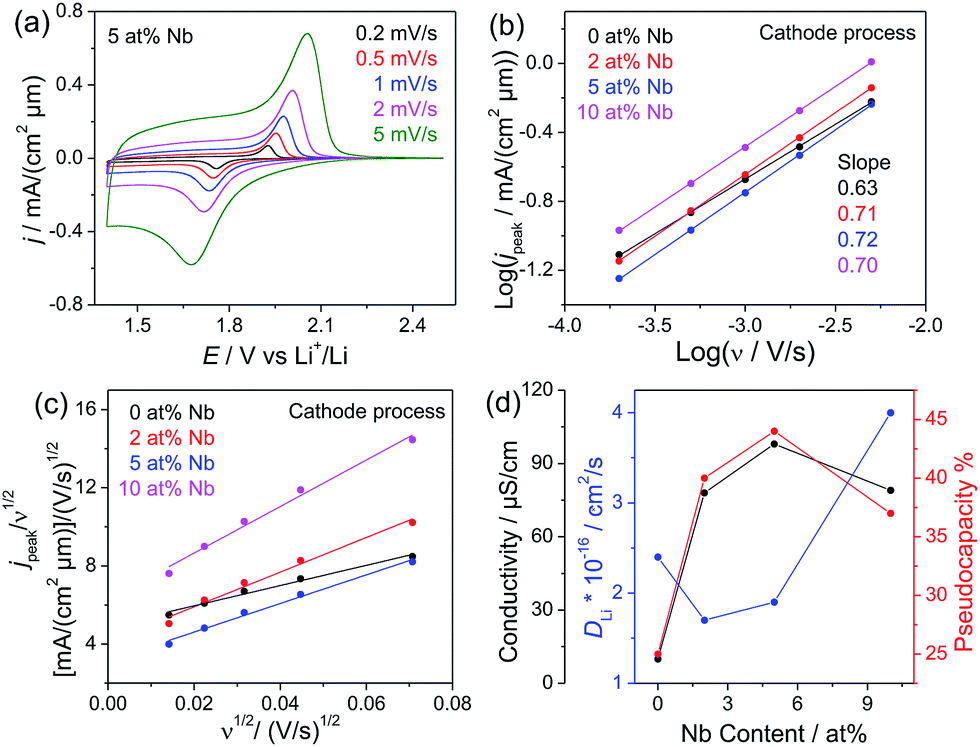 | ||
| Fig. 9 (a) Cyclic voltammograms of mesoporous 5 at% Nb:TiO2 films measured at different scanning rates. (b) Plot of log(jpeak) versus log(ν). (c) Plot of jpeak/ν1/2versus ν1/2. (d) The conductivity, pseudocapacity (values derived from the cathodic signals at the scanning rate of 1 mV s−1), and chemical diffusion coefficient of lithium as a function of the Nb content for the Nb-doped TiO2 nanoparticles. | ||
| σ/S cm−1 | b | k F | Pseudocapacity% | D Li/cm2 s−1 | |
|---|---|---|---|---|---|
| TiO2 | 1.0 × 10⁻⁵ | 0.63 | 4.9 | 25% | 2.4 × 10⁻¹⁶ |
| 2 at% | 7.8 × 10⁻⁵ | 0.71 | 4.1 | 40% | 1.7 × 10⁻¹⁶ |
| 5 at% | 9.8 × 10⁻⁵ | 0.72 | 4.3 | 44% | 1.9 × 10⁻¹⁶ |
| 10 at% | 7.9 × 10⁻⁵ | 0.70 | 6.3 | 37% | 4.0 × 10⁻¹⁶ |
Typically, analogous behavior between the storage capacity and the chemical diffusion coefficient is reported in the literature, showing that a high lithium diffusivity with a balanced electronic and ionic conductivity is beneficial for Li storage within the particles (bulk intercalation).3,62 However, at high C rates (>1C) interfacial storage is more dominant,9 thus the strong correlation between the electronic conductivity and the pseudocapacitive contribution may be attributed to the formation of a space charge layer at the surface of the mesoporous Nb:TiO2 samples. The space charge layer arises from surface states with a different Fermi level than that for the bulk material.63,64 This difference is balanced by a charge transfer resulting in an electric potential difference at the surface, band bending and the formation of a space charge region. For TiO2 in contact with a Li electrolyte the formation of the space charge region leads to a depletion of electronic charge carriers at the surface and to an accumulation (interfacial storage) of Li+ ions due to the electric potential difference between the surface and the bulk.65 As the width of the space charge layer strongly depends on the carrier concentration, changes in the carrier concentration will also affect the Li storage properties at the surface. For undoped TiO2 nanoparticles with diameters less than 10 nm the width of the space charge layer is larger than the particles themselves resulting in a negligible potential difference between the surface and the bulk.63,66 Due to the small potential difference only a low Li+ concentration accumulates at the surface as schematically shown in Fig. 10a and thus, a comparably small pseudocapacitive contribution is observed. With increasing Nb doping, the width of the space charge layer reduces, which leads to a larger surface potential in the nanosized particles as schematically shown in Fig. 10b. As a consequence, a higher Li+ concentration can accumulate at the surface and the pseudocapacitive contribution increases at low doping between 2 and 5 at%. As the Li+ concentration is only increased in the space charge layer the pseudocapacitive contribution decreases again at higher electron concentrations in the particles (10 at%) due to a further decrease of the width of the space charge layer (Fig. 10c).
 | ||
| Fig. 10 Schematic band structure and defect concentration [D] in Nb:TiO2 nanoparticles at different doping levels. | ||
4. Conclusions
Nb-doped TiO2 nanoparticles as building blocks were successfully prepared in a novel two-step solvothermal process using tert-amyl alcohol as the reactant and 1-hexanol as the co-solvent. The nanoparticles possess similar crystallite sizes and quite high dispersibility in polar solvents (10 wt% in water and 5 wt% in ethanol). Raman spectroscopy, XRD and XPS analysis suggest that the Nb5+ ions were introduced into the anatase lattice substituting Ti4+ ions, thus increasing the unit cell lattice constant and generating Ti4+ vacancies. Beyond the Nb content of 5 at%, partial Ti4+ ions become reduced to Ti3+. Mesoporous films with a uniform pore morphology were prepared by dip coating under the assistance of copolymer PIB45-b-PEO50. Conductivity measurements revealed that mesoporous films prepared from 5 at% Nb-doped TiO2 nanoparticles show the highest conductivity. The pseudocapacitive effect of mesoporous Nb-doped TiO2 films was analyzed by the peak current from cyclic voltammetry and the results indicated that the pseudocapacitive contribution to the overall charge storage correlates with the conductivity. This correlation between the conductivity and the interfacial charge storage can be explained qualitatively by considering the changes in the space charge layer at the nanoparticle surface with varying carrier concentration, which in turn depends on the doping concentration. Therefore, our study provides evidence that beyond the crystallite size and special crystallographic features17–20 a further decisive and adjust parameter needs to be taken into account and is available for designing materials with pseudocapacitive charge storage at interfaces.Still, in spite of these insights other important fundamental aspects of charge storage at/in interfaces of nanostructured materials need to be addressed in further detail, going beyond the approach of our study. For instance, our study does not take into account that the different crystal facets of TiO2 anatase correlate with different surface potentials and in turn different electronic properties at the surface, as recently pointed out by Primc et al. in a study of doping of TiO2 nanoparticles.67 Substitutional doping of Nb might affect the electronic properties, e.g. the work function, differently for the different facets of TiO2 anatase surfaces (e.g. the {101} and {001} facets).67 A further issue addresses the distribution of Nb within the material. While our SIMS analysis reveals a quite homogeneous spatial distribution of Nb on the scale of ca. 20 nm, the distribution of Nb within the nanoparticles themselves is unknown. A recent study indicated an enrichment of Nb in Nb-doped anatase TiO2, as revealed by etching of Nb-doped TiO2 followed by elemental analysis on the remaining material.68 Also, the exact value of the Nb concentration is of significant importance. As described recently by Sahasrabudhe et al., the conductivity of rutile TiO2 can be enhanced by a factor of 106 by Nb incorporation, with the conductivity depending in a highly non-linear way on the Nb content.69 In the light of these issues, future work might be devoted to the synthesis of Nb-containing TiO2 nanocrystals with a well-defined facet orientation. Meanwhile, synthetic procedures based on sol–gel chemistry are available to synthesize TiO2 nanoparticles with variable morphology and facet orientation, as recently reviewed by Darbandi et al.70
More generally, the study of pseudocapacity needs to be focused on tuning the electronic and structural properties of TiO2 nanoparticles, serving as a case study. Evidently, the surface structure of Nb:TiO2 before and after intercalation needs further investigations, which however imposes high demands on the analytical resolution. In conclusion, our study provides experimental evidence that the pseudocapacity in TiO2 nanocrystals is significantly dependent on the incorporation with Nb through modifying the band structure, which might encourage further research in understanding and designing interfacial charge storage.
Acknowledgements
We acknowledge financial support within the LOEWE program of excellence of the Federal State of Hessen (project initiative STORE-E). J. Yue is grateful for the financial support by the China Scholarship Council (CSC, #2011631008). C. S. acknowledges financial support within the SIGNO project (03SHWB073) by the German Federal Ministry for Economic Affairs and Energy (BMWi). This project was supported by the Laboratory of Materials Research (LaMa) at Justus-Liebig-University Giessen.References
- D. Wang, D. Choi, J. Li, Z. Yang, Z. Nie, R. Kou, D. Hu, C. Wang, L. V. Saraf, J. Zhang, I. A. Aksay and J. Liu, ACS Nano, 2009, 3, 907–914 CrossRef CAS PubMed.
- D. Fattakhova-Rohlfing, M. Wark, T. Brezesinski, B. M. Smarsly and J. Rathouský, Adv. Funct. Mater., 2007, 17, 123–132 CrossRef CAS.
- J.-Y. Shin, J. H. Joo, D. Samuelis and J. Maier, Chem. Mater., 2011, 24, 543–551 CrossRef.
- Y. Wang, B. M. Smarsly and I. Djerdj, Chem. Mater., 2010, 22, 6624–6631 CrossRef CAS.
- M. Fehse, S. Cavaliere, P. E. Lippens, I. Savych, A. Iadecola, L. Monconduit, D. J. Jones, J. Rozière, F. Fischer, C. Tessier and L. Stievano, J. Phys. Chem. C, 2013, 117, 13827–13835 CAS.
- S. K. Das, B. Jache, H. Lahon, C. L. Bender, J. Janek and P. Adelhelm, Chem. Commun., 2016, 52, 1428–1431 RSC.
- F. Zhao, B. Wang, Y. Tang, H. Ge, Z. Huang and H. K. Liu, J. Mater. Chem. A, 2015, 3, 22969–22974 CAS.
- H. Lindström, S. Södergren, A. Solbrand, H. Rensmo, J. Hjelm, A. Hagfeldt and S.-E. Lindquist, J. Phys. Chem. B, 1997, 101, 7717–7722 CrossRef.
- J. Y. Shin, D. Samuelis and J. Maier, Adv. Funct. Mater., 2011, 21, 3464–3472 CrossRef CAS.
- T. Brezesinski, J. Wang, J. Polleux, B. Dunn and S. H. Tolbert, J. Am. Chem. Soc., 2009, 131, 1802–1809 CrossRef CAS PubMed.
- M. Opitz, J. Yue, J. Wallauer, B. Smarsly and B. Roling, Electrochim. Acta, 2015, 168, 125–132 CrossRef CAS.
- J. Wang, J. Polleux, J. Lim and B. Dunn, J. Phys. Chem. C, 2007, 111, 14925–14931 CAS.
- M. Lubke, J. Shin, P. Marchand, D. Brett, P. Shearing, Z. Liu and J. A. Darr, J. Mater. Chem. A, 2015, 3, 22908–22914 CAS.
- M. Wagemaker, G. J. Kearley, A. A. van Well, H. Mutka and F. M. Mulder, J. Am. Chem. Soc., 2003, 125, 840–848 CrossRef CAS PubMed.
- T. C. Liu, W. G. Pell, B. E. Conway and S. L. Roberson, J. Electrochem. Soc., 1998, 145, 1882–1888 CrossRef CAS.
- J. Jamnik and J. Maier, Phys. Chem. Chem. Phys., 2003, 5, 5215–5220 RSC.
- K. Brezesinski, J. Wang, J. Haetge, C. Reitz, S. O. Steinmueller, S. H. Tolbert, B. M. Smarsly, B. Dunn and T. Brezesinski, J. Am. Chem. Soc., 2010, 132, 6982–6990 CrossRef CAS PubMed.
- V. Augustyn, J. Come, M. A. Lowe, J. W. Kim, P.-L. Taberna, S. H. Tolbert, H. D. Abruna, P. Simon and B. Dunn, Nat. Mater., 2013, 12, 518–522 CrossRef CAS PubMed.
- T. Brezesinski, J. Wang, S. H. Tolbert and B. Dunn, Nat. Mater., 2010, 9, 146–151 CrossRef CAS PubMed.
- G. A. Muller, J. B. Cook, H. S. Kim, S. H. Tolbert and B. Dunn, Nano Lett., 2015, 15, 1911–1917 CrossRef CAS PubMed.
- I. E. Rauda, V. Augustyn, B. Dunn and S. H. Tolbert, Acc. Chem. Res., 2013, 46, 1113–1124 CrossRef CAS PubMed.
- J. W. Kim, V. Augustyn and B. Dunn, Adv. Energy Mater., 2012, 2, 141–148 CrossRef CAS.
- Y. Furubayashi, T. Hitosugi, Y. Yamamoto, K. Inaba, G. Kinoda, Y. Hirose, T. Shimada and T. Hasegawa, Appl. Phys. Lett., 2005, 86, 252101 CrossRef.
- K. Xia, Q. Gao, J. Jiang and J. Hu, Carbon, 2008, 46, 1718–1726 CrossRef CAS.
- J. Huang, B. G. Sumpter and V. Meunier, Chem.–Eur. J., 2008, 14, 6614–6626 CrossRef CAS PubMed.
- P. Hartmann, D.-K. Lee, B. M. Smarsly and J. Janek, ACS Nano, 2010, 4, 3147–3154 CrossRef CAS PubMed.
- L. De Trizio, R. Buonsanti, A. M. Schimpf, A. Llordes, D. R. Gamelin, R. Simonutti and D. J. Milliron, Chem. Mater., 2013, 25, 3383–3390 CrossRef CAS.
- C. J. Dahlman, Y. Tan, M. A. Marcus and D. J. Milliron, J. Am. Chem. Soc., 2015, 137, 9160–9166 CrossRef CAS PubMed.
- Y. Liu, J. M. Szeifert, J. M. Feckl, B. Mandlmeier, J. Rathousky, O. Hayden, D. Fattakhova-Rohlfing and T. Bein, ACS Nano, 2010, 4, 5373–5381 CrossRef CAS PubMed.
- Y.-J. Zhu and F. Chen, Chem. Rev., 2014, 114, 6462–6555 CrossRef CAS PubMed.
- I. Bilecka and M. Niederberger, Nanoscale, 2010, 2, 1358–1374 RSC.
- C. Weidmann, K. Brezesinski, C. Suchomski, K. Tropp, N. Grosser, J. Haetge, B. M. Smarsly and T. Brezesinski, Chem. Mater., 2012, 24, 486–494 CrossRef CAS.
- T. von Graberg, P. Hartmann, A. Rein, S. Gross, B. Seelandt, C. Roeger, R. Zieba, A. Traut, M. Wark, J. Janek and B. M. Smarsly, Sci. Technol. Adv. Mater., 2011, 12, 025005 Search PubMed.
- J. Yue, C. Suchomski, T. Brezesinski and B. M. Smarsly, ChemNanoMat, 2015, 1, 415–421 CrossRef CAS.
- Y. Wang, T. Brezesinski, M. Antonietti and B. Smarsly, ACS Nano, 2009, 3, 1373–1378 CrossRef CAS PubMed.
- D. Bradley, R. C. Mehrotra, I. Rothwell and A. Singh, Alkoxo and aryloxo derivatives of metals, Academic Press, London, 2001 Search PubMed.
- A. M. Ruiz, G. Dezanneau, J. Arbiol, A. Cornet and J. R. Morante, Chem. Mater., 2004, 16, 862–871 CrossRef CAS.
- W. F. Zhang, Y. L. He, M. S. Zhang, Z. Yin and Q. Chen, J. Phys. D: Appl. Phys., 2000, 33, 912–916 CrossRef CAS.
- T. Ohsaka, F. Izumi and Y. Fujiki, J. Raman Spectrosc., 1978, 7, 321–324 CrossRef.
- F. Tian, Y. Zhang, J. Zhang and C. Pan, J. Phys. Chem. C, 2012, 116, 7515–7519 CAS.
- X. Lü, W. Yang, Z. Quan, T. Lin, L. Bai, L. Wang, F. Huang and Y. Zhao, J. Am. Chem. Soc., 2014, 136, 419–426 CrossRef PubMed.
- X. Lü, X. Mou, J. Wu, D. Zhang, L. Zhang, F. Huang, F. Xu and S. Huang, Adv. Funct. Mater., 2010, 20, 509–515 CrossRef.
- T. Leichtweiss, R. A. Henning, J. Koettgen, R. M. Schmidt, B. Hollander, M. Martin, M. Wuttig and J. Janek, J. Mater. Chem. A, 2014, 2, 6631–6640 CAS.
- D. S. Bhachu, S. Sathasivam, G. Sankar, D. O. Scanlon, G. Cibin, C. J. Carmalt, I. P. Parkin, G. W. Watson, S. M. Bawaked, A. Y. Obaid, S. Al-Thabaiti and S. N. Basahel, Adv. Funct. Mater., 2014, 24, 5075–5085 CrossRef CAS.
- B. Mei, M. D. Sanchez, T. Reinecke, S. Kaluza, W. Xia and M. Muhler, J. Mater. Chem., 2011, 21, 11781–11790 RSC.
- T. Hitosugi, H. Kamisaka, K. Yamashita, H. Nogawa, Y. Furubayashi, S. Nakao, N. Yamada, A. Chikamatsu, H. Kumigashira and M. Oshima, Appl. Phys. Express, 2008, 1, 111203 CrossRef.
- S. Zhang, S. B. Ogale, W. Yu, X. Gao, T. Liu, S. Ghosh, G. P. Das, A. T. S. Wee, R. L. Greene and T. Venkatesan, Adv. Mater., 2009, 21, 2282–2287 CrossRef CAS.
- L. R. Sheppard, T. Dittrich and M. K. Nowotny, J. Phys. Chem. C, 2012, 116, 20923–20929 CAS.
- T. Nikolay, L. Larina, O. Shevaleevskiy and B. T. Ahn, Energy Environ. Sci., 2011, 4, 1480–1486 CAS.
- M. Thommes, K. Kaneko, A. V. Neimark, J. P. Olivier, F. Rodriguez-Reinoso, J. Rouquerol and K. S. Sing, Pure Appl. Chem., 2015, 87, 1051–1069 CrossRef CAS.
- M. Thommes, B. Smarsly, M. Groenewolt, P. I. Ravikovitch and A. V. Neimark, Langmuir, 2006, 22, 756–764 CrossRef CAS PubMed.
- P. A. Monson, Microporous Mesoporous Mater., 2012, 160, 47–66 CrossRef CAS.
- C. Reitz, J. Reinacher, P. Hartmann and T. Brezesinski, Catal. Today, 2014, 225, 55–63 CrossRef CAS.
- P. S. Archana, R. Jose, M. M. Yusoff and S. Ramakrishna, Appl. Phys. Lett., 2011, 98, 152106 CrossRef.
- H. J. Snaith and L. Schmidt-Mende, Adv. Mater., 2007, 19, 3187–3200 CrossRef CAS.
- T. Brezesinski, J. Wang, S. H. Tolbert and B. Dunn, J. Sol-Gel Sci. Technol., 2011, 57, 330–335 CrossRef CAS.
- V. Augustyn, P. Simon and B. Dunn, Energy Environ. Sci., 2014, 7, 1597–1614 CAS.
- K. Zhu, Q. Wang, J.-H. Kim, A. A. Pesaran and A. J. Frank, J. Phys. Chem. C, 2012, 116, 11895–11899 CAS.
- B. Hao, Y. Yan, X. Wang and G. Chen, ACS Appl. Mater. Interfaces, 2013, 5, 6285–6291 CAS.
- Y. Yan, B. Hao, D. Wang, G. Chen, E. Markweg, A. Albrecht and P. Schaaf, J. Mater. Chem. A, 2013, 1, 14507–14513 CAS.
- M. Bousa, B. Laskova, M. Zukalova, J. Prochazka, A. Chou and L. Kavan, J. Electrochem. Soc., 2010, 157, A1108–A1112 CrossRef CAS.
- J.-Y. Shin, J. H. Joo, K. K. Adepalli, D. Samuelis and J. Maier, Phys. Chem. Chem. Phys., 2016, 18, 8963–8970 RSC.
- Z. Zhang and J. T. Yates, Chem. Rev., 2012, 112, 5520–5551 CrossRef CAS PubMed.
- R. T. Tung, Mater. Sci. Eng., R, 2001, 35, 1–138 CrossRef.
- C. Li, L. Gu, X. Guo, D. Samuelis, K. Tang and J. Maier, Nano Lett., 2012, 12, 1241–1246 CrossRef CAS PubMed.
- K. Ozawa, M. Emori, S. Yamamoto, R. Yukawa, S. Yamamoto, R. Hobara, K. Fujikawa, H. Sakama and I. Matsuda, J. Phys. Chem. Lett., 2014, 5, 1953–1957 CrossRef CAS PubMed.
- D. Primc, G. Zeng, R. Leute, M. Walter, L. Mayrhofer and M. Niderberger, Chem. Mater., 2016, 28, 4223–4230 CrossRef CAS.
- M. M. Yildizhan, S. Sturm and M. A. Gulgun, J. Mater. Sci., 2016, 51, 5912–5923 CrossRef CAS.
- G. Sahasrabudhe, J. Krizan, S. L. Bergman, R. J. Cava and J. Schwartz, Chem. Mater., 2016, 28, 3630–3633 CrossRef.
- M. Darbandi and J. H. Dickerson, Mater. Lett., 2016, 180, 212–218 CrossRef CAS.
Footnote |
| † Electronic supplementary information (ESI) available: The XRD and TGA of the as-prepared nanoparticles, high-resolution TEM images, the refined structural parameters, UV-visible absorption spectra, SEM images of mesoporous films, etc. See DOI: 10.1039/c6ta06840e |
| This journal is © The Royal Society of Chemistry 2017 |