
Activation of a particulate Ta3N5 water-oxidation photoanode with a GaN hole-blocking layer†
Yusuke
Asakura‡
 a,
Tomohiro
Higashi
a,
Hiroshi
Nishiyama
a,
Hiroyuki
Kobayashi
bc,
Mamiko
Nakabayashi
d,
Naoya
Shibata
d,
Tsutomu
Minegishi
ae,
Takashi
Hisatomi
a,
Masao
Katayama
a,
Taro
Yamada
a and
Kazunari
Domen
*a
a,
Tomohiro
Higashi
a,
Hiroshi
Nishiyama
a,
Hiroyuki
Kobayashi
bc,
Mamiko
Nakabayashi
d,
Naoya
Shibata
d,
Tsutomu
Minegishi
ae,
Takashi
Hisatomi
a,
Masao
Katayama
a,
Taro
Yamada
a and
Kazunari
Domen
*a
aDepartment of Chemical System Engineering, The University of Tokyo, 7-3-1 Hongo, Bunkyo-ku, Tokyo 113-8656, Japan. E-mail: domen@chemsys.t.u-tokyo.ac.jp
bJapan Technological Research Association of Artificial Photosynthetic Chemical Process, 2-11-9 Iwamotocho, Chiyoda-ku, Tokyo 101-0032, Japan
cFujifilm Corporation, 577 Ushijima, Kaisei-Machi, Ashigarakami-gun, Kanagawa 258-8577, Japan
dInstitute of Engineering Innovation, The University of Tokyo, 2-11-16 Yayoi, Bunkyo-ku, Tokyo 113-8656, Japan
eJapan Science and Technology Agency/Precursory Research for Embryonic Science and Technology (JST/PRESTO), Kawaguchi Center Building, 4-1-8 Honcho, Kawaguchi-shi, Saitama 332-0012, Japan
First published on 13th October 2017
Abstract
Particulate Ta3N5, a material that responds to visible light for photoelectrochemical O2 evolution, was glued to a metallic GaN conducting layer. The electrode was able to oxidize water with 1.8-fold higher efficiency than that without GaN. The GaN layer blocked the hole current from Ta3N5 to the back-contact metal layer and prevented hole–electron recombination.
Sunlight-driven hydrogen evolution by water splitting is one of the most rational solutions for today's worldwide problem of fossil fuel exhaustion. Photoelectrochemical (PEC) water splitting on semiconductor electrodes is an efficient method because the energy of sunlight can be directly converted into chemical energy.1 In this sense, research should be performed for semiconductors with the potentiality to realize high solar-to-hydrogen conversion efficiency.
Some transition metal nitrides and oxynitrides (e.g., Ta3N5,2 LaTiO2N,3 BaTaO2N,4 SrNbO2N,5 and BaNbO2N5c) are attractive types of photocatalysts and photoanodes for water splitting. These materials possess optical absorption spectra spreading to the visible region and are n-type semiconductors, which are suitable for oxygen evolution from water. Not many semiconducting oxides can absorb and utilize visible light, compared to those with nitrogen-containing materials.
Among such semiconductors, Ta3N5, having an optical absorption band spreading up to 600 nm, is one of the most promising photoanodic materials. The narrow band gap (2.1 eV) is induced by the shallow potential of the valence band maximum consisting of only N 2p orbitals. It was recently reported that a Ta3N5 film via NaTaO3 on a Ta substrate exhibited a photocurrent of 12.5 mA cm−2 at 1.23 VRHE under AM1.5G-simulated sunlight illumination (1 sun). Indeed, Ta3N5 has great potential for water oxidation.6 However, the method for fabricating the film is not suitable for mass-scale production of photoelectrodes, for example, to build a solar hydrogen plant. In the scalable process of constructing a light-absorbing device, a more optimal material to use for fabricating photoanodes is particulate Ta3N5 powder.
Although various strategies have been devised to utilize particulate Ta3N5 for highly active photoelectrodes, its performance has not exceeded that of film electrodes.6,7 To utilize Ta3N5 powder, a certain structure for the light absorption sheet and methods for fabrication should be found. The “particle transfer method”3a is the most advanced manoeuvre to utilize photoactive powder for making a planar, electrically conductive, light-absorbing plate. A particle-transfer photoelectrode is composed of photoactive particles evaporated with a metallic layer for good electronic contact as well as a conductor layer for good carrier transport to the lead wire. These metallic layers also mechanically fix the grains and are commonly glued on a firm substrate such as a glass plate. On the surface of such a plate is a photoactive particle monolayer that is open to contact with the electrolytic solution, whereas the backside is composed of a semiconductor-to-metal junction, providing low-resistance carrier transport.
One method to improve the performance of the photoanode, made of an n-type semiconductor, is to refine the back contact. The choice of conductive layer metals3a,8 and/or the insertion of another semiconductor material between the photoanode material and the conductive layer will certainly enhance the anodic photocurrent.9 It is anticipated that an effective method is to use a hole-blocking layer, defined as a semiconductor that has a deep position of the valence band top and is formed between the photoanode material and the carrier conduction layer. By the deep valence band position, the excited holes in the photoanodic material cannot transfer to the current conduction layer, whereas transfer occurs for the excited electrons. By this mechanism, the electron–hole recombination can be prevented and an enhanced photocurrent can be expected.9c The application of such a strategy for particulate nitrides/oxynitrides will successfully improve the photocurrent, and methods to introduce a hole-blocking layer between the particles and the conductive metallic layer should be pursued.
In this report, a GaN layer was introduced between Ta3N5 particles and back contact metallic layers (Ta), and the layered structure (Ta3N5/GaN) resulted in a large increase in photocurrent. In the case of Ta3N5/Ta without GaN, excited holes and electrons in Ta3N5 can recombine in the back contact metallic layer (Fig. 1a). The top position of the valence band of GaN is much deeper than that of Ta3N5, while the conduction band of GaN is located at a comparable potential to that of Ta3N5.10 Therefore, the GaN layer as a back contact for Ta3N5 can act as a hole-blocking layer to prevent recombination between excited holes and electrons, because the excited holes in Ta3N5 cannot easily transfer to the conductive layer. Some oxides including Ta2O5 (ref. 10b) possess a suitable band structure for such a hole-blocking layer. However, when we prepared an oxide layer with crystallinity behind powdered Ta3N5, the Ta3N5 oxidized to a certain degree because of the high temperature for crystallization. Therefore, we introduced a nitride layer with a suitable band structure, GaN, to prevent oxidation of Ta3N5. Additionally, the introduction of a hole-storage layer on the electrode surface improved the photocurrent density and stability.6,11 The layer can accumulate excited holes on the surface under light illumination to spatially separate excited holes and electrons, and can further prevent recombination between excited holes and electrons. Therefore, we prepared an electrode with not only a hole-blocking layer but also a hole-storage layer in the particulate Ta3N5 electrode (Fig. 1b).
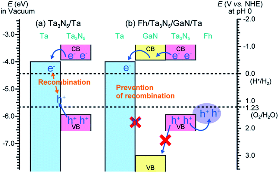 | ||
| Fig. 1 Schematic band view of the laminated structure of (a) Ta3N5/Ta and (b) Fh/Ta3N5/GaN/Ta. This view is described on the basis of the two previous reports.10 | ||
The photoanode of Ta3N5/GaN was prepared by a combination of the particle-transfer (PT) method3a and the plasma-enhanced chemical vapor deposition method12 (Scheme 1, also shown in the ESI†). The experimental procedure is composed of 5 steps.
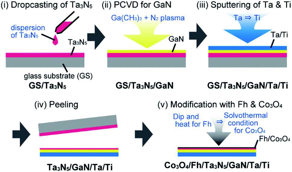 | ||
| Scheme 1 Synthetic procedure of the Ta3N5 electrode with GaN as a hole-blocking layer and modification with ferrihydrite (Fh) and Co3O4. | ||
(i) A dispersion of Ta3N5 (ref. 2) in 2-propanol was dropped on the glass substrate (GS) to form thick powder layers after drying of the solvent (the XRD datum, the UV-DRS spectrum, and the SEM images of Ta3N5 powder are shown in Fig. S1 and S2;† the average size of the particles is approximately 1 μm).
(ii) A GaN layer (approximately 30 nm) was deposited by plasma-enhanced chemical vapor deposition (PCVD) with trimethylgallium and nitrogen plasma. A deposition temperature of 500 °C was mainly used.
(iii) A Ta metal contact layer (approximately 100 nm) and then a Ti metal conductor layer (more than 5 μm) were further deposited using radio frequency magnetron sputtering to form a laminated sample (GS/Ta3N5/GaN/Ta/Ti).
(iv) The laminated sample was peeled from the glass substrate and sonicated in distilled water to remove the excess Ta3N5 particles on the surface.
(v) Deposition of an electrode consisting of ferrihydrite (Fh) as a hole-storage layer followed by Co3O4 as an oxygen evolution catalyst was accomplished through successive steps that included a dipping and heating treatment and solvothermal treatment according to a previous report11a to form Co3O4/Fh/Ta3N5/GaN/Ta/Ti.
The SEM image of the surface of the Ta3N5/GaN/Ta/Ti electrode (Fig. 2a) is almost the same as the SEM image of Ta3N5 powder without any coating (Fig. S2†). Careful inspection of these images reveals the existence of small holes (diameter approximately a few tens of nanometers) on the surfaces of Ta3N5 grains. Inversely to Fig. 1a, for SEM observation, a GaN/Ta3N5/Ta/Ti sample was prepared by plasma CVD of GaN on Ta3N5/Ta/Ti under the same condition. The top view of GaN/Ta3N5/Ta/Ti (Fig. 2b) involves grainy surfaces of Ta3N5 particles, which were created by the deposition of GaN species. One notable finding is the disappearance of the small holes observed on bare Ta3N5 particles.
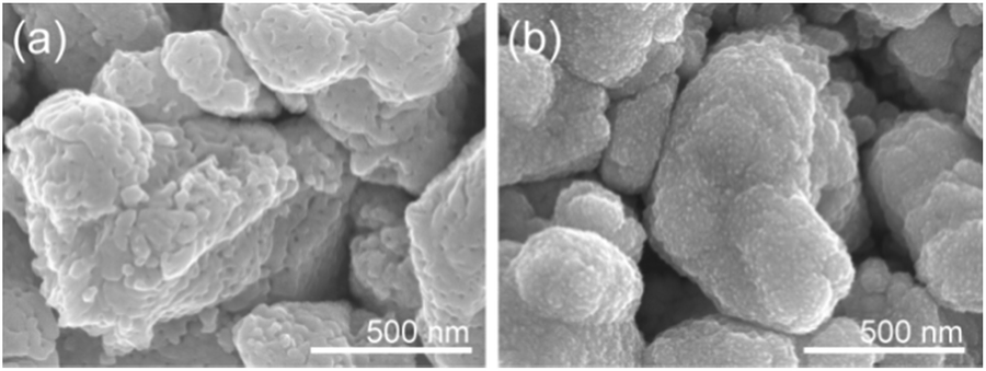 | ||
| Fig. 2 SEM images of the surfaces of (a) Ta3N5/GaN/Ta/Ti and (b) GaN/Ta3N5/Ta/Ti. | ||
Cross-sectional TEM observations were conducted for Ta3N5/Ta/Ti and Ta3N5/GaN/Ta/Ti. The high-resolution (HR) TEM and annular dark field (ADF) STEM images of Ta3N5/Ta/Ti (Fig. S3† and 3a) show a three-layer laminated structure. The parts of the outermost electrode surfaces (the left side of the TEM images) contain grains of Ta3N5. The STEM-EDS mapping (Fig. 3b) clarifies that the other two layers under (i.e., to the right of) the Ta3N5 particle are the laminated structures of Ta and Ti. This result indicates that the ideal structure of Ta3N5/Ta/Ti was successfully obtained. The HRTEM and ADF STEM images of Ta3N5/GaN/Ta/Ti (Fig. 3c and d) show a similar laminated structure to that of Ta3N5/Ta/Ti. A high-magnification HRTEM image (Fig. 3e) shows Ta3N5/GaN/Ta/Ti involving one more layer adhered to a Ta3N5 grain. The STEM-EDS mapping of Ta3N5/GaN/Ta/Ti (Fig. 3f) clarifies that the layer includes Ga species between Ta3N5 grains and the Ta contact layer. The present strategy of inserting PCVD GaN between Ta3N5 particles and the back contact Ti layer was successful. Cross sections of electrodes after deposition of ferrihydrite and Co3O4 (Co3O4/Fh/Ta3N5/GaN/Ta/Ti) were also analysed by TEM (Fig. S4†). In general, they were not morphologically different from samples without Co3O4/Fh, and elementary mappings (Fig. S4c–g and j†) for Co and Fe did not appear concentrated in a special position in the cross section. The successive Co3O4/Fh treatment did not disturb the microscopic laminated structure. The laminated electrode possessed GaN behind the Ta3N5 particles with a size of several hundred nanometers, as clearly indicated in the STEM-EDS mapping (Fig. 3f). Because the value of the absorption coefficient for Ta3N5 is greater than 4 × 10⁻⁵ cm−1 for the UV light wavelength,13 UV light can penetrate a Ta3N5 particle only by up to several-ten nanometers and cannot reach the GaN layer located behind the Ta3N5 particles. This indicates that GaN should not play a role as an absorber in this laminated electrode.
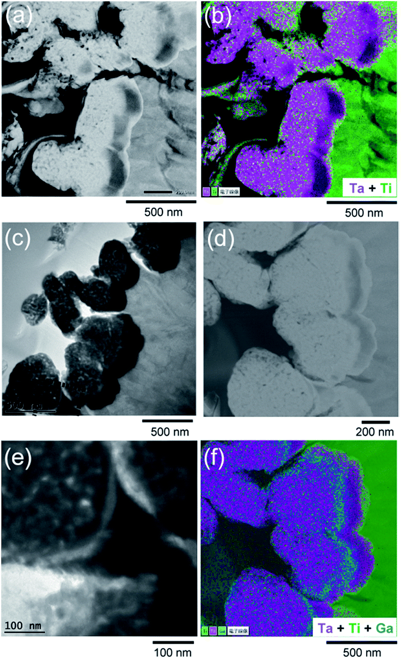 | ||
| Fig. 3 (a) Annular dark field (ADF) STEM image and (b) STEM-EDS mapping of a cross section of Ta3N5/Ta/Ti, and (c) high-resolution (HR) TEM and (d) ADF STEM images, and (e) HRTEM image of the selected square area of the image (c), and (f) STEM-EDS mapping of the cross section of Ta3N5/GaN/Ta/Ti. The left sides of these images show the surface of the electrodes. Purple, green, and aqua in the STEM-EDS mappings (b and f) denote the regions of tantalum, titanium, and gallium, respectively. | ||
Current–potential (I–E) curves under simulated AM1.5G irradiation of Co3O4/Fh/Ta3N5/GaN/Ta/Ti and Co3O4/Fh/Ta3N5/Ta/Ti are shown in Fig. 4A. The anodic photocurrent of both electrodes was generated above 0.8 VRHE, indicating no difference in onset potential. The photocurrent of Co3O4/Fh/Ta3N5/GaN/Ta/Ti is higher than that of Co3O4/Fh/Ta3N5/Ta/Ti at all potentials above 0.8 VRHE (especially 4.2 mA cm−2 and 3.0 mA cm−2, respectively, at 1.23 VRHE). The onset potential is more positive than that expected from the band structure. This behaviour probably occurred because of two reasons: (i) high overpotential of water oxidation and (ii) recombination between excited electrons and holes on the defects. When a photoanode is composed of nitrides/oxynitrides, it is more likely that reason (ii) should be dominant as compared to when other types of materials are used, because nitrogen defects on the surface can easily be formed. The half-cell solar-to-hydrogen (HC-STH) conversion efficiency of Co3O4/Fh/Ta3N5/GaN/Ta/Ti reached 0.43% at 1.0 VRHE, which is 1.8 times as high as that of Co3O4/Fh/Ta3N5/Ta/Ti (0.24% at 1.1 VRHE) (inset of Fig. 4A). M. Zhong et al. reported that a GaN layer on Ta3N5 thin film can improve the photocurrent and stability of a Ta3N5 thin-film electrode,7 although the relationship of the GaN layer and Ta3N5 is opposite to that in the case of the present study. It is known that the nature of GaN is altered by its synthetic procedure. The GaN layer in the previous report by M. Zhong et al. was synthesized by post NH3 nitridation of the GaOx layer by electron-beam physical vapour deposition. However, the GaN layer in the current study was directly synthesized by plasma-enhanced CVD. The layer contained a small amount of oxygen, as shown in the XPS spectra of the layer (Fig. S5†). This synthetic procedure should lead to a difference in various conditions of the GaN layer including the number of defects and impurities (e.g. oxygen), crystallinity, and crystal growth direction. The differences will be investigated in the near future.
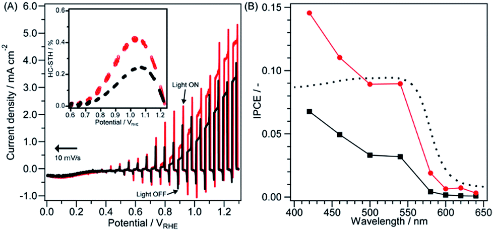 | ||
| Fig. 4 (A) I–E curves (inset of A), HC-STH conversion efficiencies, and (B) wavelength dependences of IPCE at 1.0 VRHE for Co3O4/Fh/Ta3N5/Ta/Ti (black line and marks) and Co3O4/Fh/Ta3N5/GaN/Ta/Ti (red line and marks) with an absorption spectrum of Ta3N5 (dashed line). The I–E curves were acquired with a 0.2 M K2HPO4 solution adjusted to pH 13 by adding KOH. The applied potential was swept with −10 mV s−1 under intermittent irradiation of simulated AM1.5G light. The IPCE was also acquired in the same solution by using monochromatic lights at 1.0 VRHE. | ||
Although it was reported that Fh in the presence of a Ta3N5 film electrode led to a decrease in the photocurrent,11a the deposition of Fh on a particulate Ta3N5 electrode (Ta3N5/Ta/Ti) in this work was effective for enhancement of the anodic photocurrent, with or without the back-contact GaN layer (Fig. S6†). Therefore, the successive deposition of Fh and Co3O4 was applied for all the electrodes shown here.
The incident photon-to-current conversion efficiency (IPCE) of Co3O4/Fh/Ta3N5/GaN/Ta/Ti is also approximately twice as high as that of Co3O4/Fh/Ta3N5/Ta/Ti over the absorbable light region of Ta3N5 (up to 600 nm) (Fig. 4B). The IPCEs of the electrodes indicate that the efficiencies were increased from 600 nm to even below 500 nm, although the absorption of Ta3N5 was saturated to 550 nm. This behaviour probably occurs because the shorter penetration depth of light irradiation with a shorter wavelength enables the high carrier density found on the interface between the electrode and electrolyte. These results indicate that the deposition of GaN as a back contact for a particulate Ta3N5 photoanode is significantly effective for enhancement of anodic photocurrent. Recently, it was reported that Co species can work as a light-sensitizing material to induce photocatalytic/photoelectrochemical water oxidation with light irradiation above 800 nm.14 However, in this study, IPCE was not observed above 600 nm, which is consistent with an absorption spectrum of Ta3N5 including no cocatalyst (Fig. S1b†). This indicates that the Co3O4 in our case worked poorly as a light absorber.
Fig. 5 shows the time course of the photocurrent and the amounts of evolved gases obtained from the photoanodes of Co3O4/Fh/Ta3N5/Ta/Ti and Co3O4/Fh/Ta3N5/GaN/Ta/Ti under simulated AM1.5G light irradiation. A CrOx-coated Pt mesh was employed as a counter electrode for H2 evolution in order to suppress the reverse reaction of evolved gases to water on the Pt surface. The current–time (I–t) curves recorded at 1.0 VRHE clearly demonstrated that the photocurrent of Co3O4/Fh/Ta3N5/GaN/Ta/Ti remained higher than that of Co3O4/Fh/Ta3N5/Ta/Ti even after 120 min of light irradiation (Fig. 5Aa and Ba). The ratios of the evaluated H2 and O2 were constantly 2![[thin space (1/6-em)]](https://www.rsc.org/images/entities/char_2009.gif) :1 for both photoanodes, indicating stoichiometric water splitting. The obtained gas amounts from Co3O4/Fh/Ta3N5/GaN/Ta/Ti were approximately twice as much as that from Co3O4/Fh/Ta3N5/Ta/Ti (Fig. 5Ab and Bb). The faradaic efficiencies of Co3O4/Fh/Ta3N5/Ta/Ti and Co3O4/Fh/Ta3N5/GaN/Ta/Ti are 96% and 93%, respectively. The faradaic efficiencies are slightly low, presumably because of partial oxidation of Ta3N5 itself during water oxidation.
:1 for both photoanodes, indicating stoichiometric water splitting. The obtained gas amounts from Co3O4/Fh/Ta3N5/GaN/Ta/Ti were approximately twice as much as that from Co3O4/Fh/Ta3N5/Ta/Ti (Fig. 5Ab and Bb). The faradaic efficiencies of Co3O4/Fh/Ta3N5/Ta/Ti and Co3O4/Fh/Ta3N5/GaN/Ta/Ti are 96% and 93%, respectively. The faradaic efficiencies are slightly low, presumably because of partial oxidation of Ta3N5 itself during water oxidation.
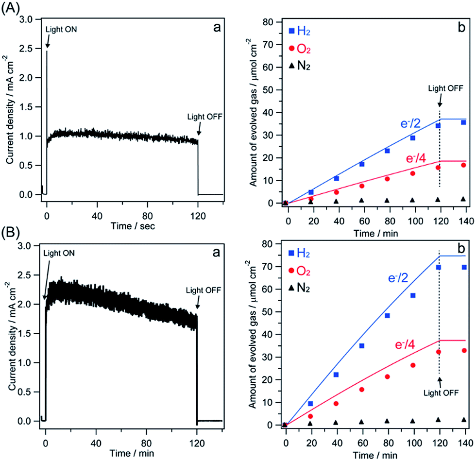 | ||
| Fig. 5 (a) I–t curves and (b) the plots for the amounts of the evolved gases (H2, O2, and N2) for Co3O4/Fh/Ta3N5/Ta/Ti (A) and a Co3O4/Fh/Ta3N5/GaN/Ta/Ti (B) recorded at 1.0 VRHE under simulated AM 1.5G light irradiation. A 0.2 M K2HPO4 solution adjusted to pH 13 by adding KOH was used as an electrolyte. The blue and red lines in (b) indicate the expected gas amounts of H2 and O2, respectively, calculated from the total charge recorded as the photocurrent. | ||
To determine the photoelectrode performance based on the quality of the GaN layer, PCVD GaN was deposited at several different temperatures, and I–E curves were recorded. The I–E curves for Co3O4/Fh/Ta3N5/GaN/Ta/Ti are shown in Fig. 6. The photocurrents of the electrodes with GaN deposited at 300, 400, and 600 °C were 2.9, 3.8, and 4.1 mA cm−2 at 1.23 VRHE, respectively. The electrode with GaN deposited at 300 °C exhibited a lower photocurrent than that without GaN. However, when the deposition was performed at 400 and 600 °C, the corresponding electrodes were improved. The photocurrent was the largest for the standard samples deposited at 500 °C.
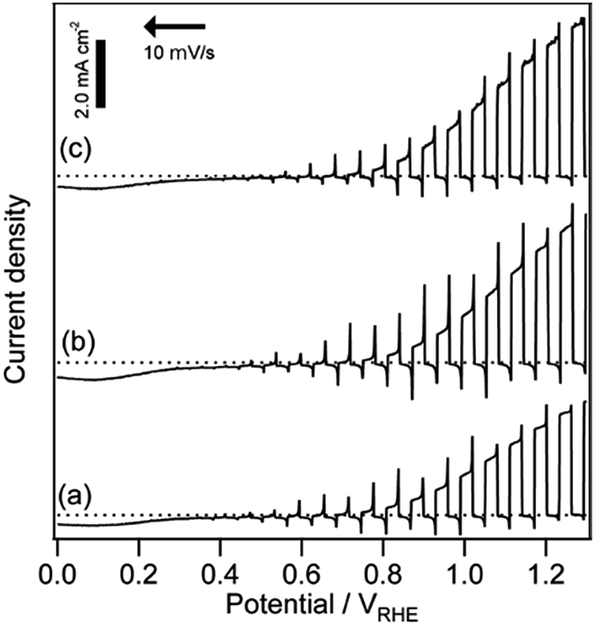 | ||
| Fig. 6 I–E curves of Co3O4/Fh/Ta3N5/Ta/Ti with a GaN layer deposited at (a) 300, (b) 400, and (c) 600 °C. The I–E curves were acquired with a 0.2 M K2HPO4 solution adjusted to pH 13 by adding KOH. The applied potential was swept with −10 mV s−1 under intermittent irradiation of simulated AM1.5G light. | ||
The effect of the GaN deposition temperature can be linked to the crystallinity of the GaN film. We performed XRD analysis for GaN thin films (thickness 150 nm) on sapphire (001) substrate at various temperatures for a longer time (20 min) under the same conditions as those for the Ta3N5 particle. According to the XRD peak intensity for GaN (002) diffraction, the 500 °C sample exhibited the most optimal crystallinity (Fig. S7†). The crystallinity coincides with the order of the photocurrents shown in the photoelectrochemical curves. Although the conditions of GaN deposition including temperature and pressure were regulated by the specification of the PCVD machine in this study, improved quality GaN as a back contact will lead to further improvement of photoanodic properties.
To understand the role of GaN as the back contact, the Mott–Schottky (MS) plots of Ta3N5/Ta/Ti and Ta3N5/GaN/Ta/Ti with GaN deposited at 500 °C were compared (Fig. S8†). The slope of the plot for Ta3N5/GaN/Ta/Ti is steeper than that for Ta3N5/Ta/Ti. The slope of the MS plot is inversely proportional to the donor density. This result indicates that Ta3N5/GaN/Ta/Ti possesses a lower donor density, and therefore, a higher resistance than Ta3N5/Ta/Ti. A higher electric resistance can retard both the conversion of excited carriers to current, and the recombination of excited carriers. In the present case, judging from the high performance of the electrode, the charge recombination process must be dominantly depleted.
Efficient prevention of carrier recombination can be linked to the hole-blocking effect of the GaN layer, which has an apparently deeper position than that of Ta3N5 in terms of the valence band top as shown in Fig. 1. This effect is analogical to that of a previously reported SnO2 layer for BiVO4 thin-film electrodes.9c For Ta3N5/Ta/Ti, the excited holes in Ta3N5 can easily diffuse to the back contact Ta and more frequently combine with electrons therein. However, in the case of Ta3N5/GaN/Ta/Ti, it is very difficult for the excited holes in Ta3N5 to move to Ta because of the GaN hole-blocking potential barrier. The excited electrons in Ta3N5 can then easily transfer to Ta because of the comparable conduction location of GaN with that of Ta3N5. This is a plausible mechanism for suppression of charge recombination. In addition, the ferrihydrite on the particulate Ta3N5 electrode can effectively conduct high photocurrent. The hole-storage ability of ferrihydrite should lead to the trapping of excited holes on the electrode surface to induce band bending on the liquid–electrode interface.11a Consequently, introduction of both the hole-storage layer and the hole-blocking layer facilitates the spatial separation of excited holes and electrons to a large degree.
Conclusions
The introduction of GaN as a hole-blocking layer for a particulate Ta3N5 photoanode largely increased its photoanodic current for water oxidation. The efficiency of the water oxidation of the Ta3N5 electrode with GaN was 1.8-fold higher than that without GaN. Combining the particle transfer method with the PCVD method led to the successful preparation of the Ta3N5/GaN/Ta/Ti electrode. In addition, the temperature of the GaN-coating process by PCVD affected the photocurrent. More sophisticated conditions for GaN coating by PCVD will lead to further improvement of the photocurrent. The strategy shown here to prepare an electrode with particulate semiconductor layers can be applied to other particulate semiconductors to enhance their photoelectrochemical performances.Conflicts of interest
There are no conflicts to declare.Acknowledgements
The authors are grateful to Mr T. Iyama, Dr Y. Kobayashi, and Mr H. Shibano for their assistance with experiments. This work was financially supported by the Artificial Photosynthesis Project for the New Energy and Industrial Technology Development Organization (NEDO). A part of this work was conducted at the Advanced Characterization Nanotechnology Platform of the University of Tokyo, supported by the “Nanotechnology Platform” of the Ministry of Education, Culture, Sports, Science and Technology (MEXT), Japan.Notes and references
-
(a) A. Kudo and Y. Miseki, Chem. Soc. Rev., 2009, 38, 253 RSC
; (b) M. G. Walter, E. L. Warren, J. R. McKone, S. W. Boettcher, Q. Mi, E. A. Santori and N. S. Lewis, Chem. Rev., 2010, 110, 6446 CrossRef CAS PubMed
- M. Higashi, K. Domen and R. Abe, Energy Environ. Sci., 2011, 4, 4138 CAS
-
(a) T. Minegishi, N. Nishimura, J. Kubota and K. Domen, Chem. Sci., 2013, 4, 1120 RSC
-
(a) K. Ueda, T. Minegishi, J. Clune, M. Nakabayashi, T. Hisatomi, H. Nishiyama, M. Katayama, N. Shibata, J. Kubota, T. Yamada and K. Domen, J. Am. Chem. Soc., 2015, 137, 2227 CrossRef CAS PubMed
-
(a) H. Urabe, T. Hisatomi, T. Minegishi, J. Kubota and K. Domen, Faraday Discuss., 2014, 176, 213 RSC
- G. J. Liu, S. Ye, P. L. Yan, F. Q. Xiong, P. Fu, Z. L. Wang, Z. Chen, J. Y. Shi and C. Li, Energy Environ. Sci., 2016, 9, 1327 CAS
- M. Zhong, T. Hisatomi, Y. Sasaki, S. Suzuki, K. Teshima, M. Nakabayashi, N. Shibata, H. Nishiyama, M. Katayama, T. Yamada and K. Domen, Angew. Chem., Int. Ed., 2017, 56, 4739 CrossRef CAS PubMed
- C. Wang, T. Hisatomi, T. Minegishi, M. Nakabayashi, N. Shibata, M. Katayama and K. Domen, Chem. Sci., 2016, 7, 5821 RSC
-
(a) J. Su, L. Guo, N. Bao and C. A. Grimes, Nano Lett., 2011, 11, 1928 CrossRef CAS PubMed
-
(a) V. J. Babu, S. Vempati, T. Uyar and S. Ramakrishna, Phys. Chem. Chem. Phys., 2015, 17, 2960 RSC
-
(a) G. J. Liu, J. Y. Shi, F. X. Zhang, Z. Chen, J. F. Han, C. M. Ding, S. S. Chen, Z. L. Wang, H. X. Han and C. Li, Angew. Chem., Int. Ed., 2014, 53, 7295 CrossRef CAS PubMed
-
(a) D. C. Park, S. Fujita and S. Fujita, J. Mater. Sci. Lett., 2000, 19, 631 CrossRef CAS
-
(a) A. Ziani, E. Nurlaela, D. S. Dhawale, D. A. Silva, E. Alarousu, O. F. Mohammed and K. Takanabe, Phys. Chem. Chem. Phys., 2015, 17, 2670 RSC
-
(a) K. Maeda, K. Ishimaki, Y. Tokunaga, D. L. Lu and M. Eguchi, Angew. Chem., Int. Ed., 2016, 55, 8309 CrossRef CAS PubMed
Footnotes |
| † Electronic supplementary information (ESI) available: Experimental details and the additional results. See DOI: 10.1039/c7se00402h |
| ‡ Present address: Institute of Multidisciplinary Research for Advanced Materials (IMRAM), Tohoku University, 2-1-1 Katahira, Aoba-ku, Sendai 980-8577, Japan. |
| This journal is © The Royal Society of Chemistry 2018 |