
 Open Access Article
 This Open Access Article is licensed under a Creative Commons Attribution-Non Commercial 3.0 Unported Licence
Optimization of a compact layer of TiO2via atomic-layer deposition for high-performance perovskite solar cells†
Ahmed Esmail
Shalan
a,
Sudhakar
Narra
b,
Tomoya
Oshikiri
 a,
Kosei
Ueno
a,
Xu
Shi
a,
Hui-Ping
Wu
b,
Mahmoud M.
Elshanawany
b,
Eric
Wei-Guang Diau
*b and
Hiroaki
Misawa
*ab
a,
Kosei
Ueno
a,
Xu
Shi
a,
Hui-Ping
Wu
b,
Mahmoud M.
Elshanawany
b,
Eric
Wei-Guang Diau
*b and
Hiroaki
Misawa
*ab
aResearch Institute for Electronic Science, Hokkaido University, N21, W10, Kita-ku, 001-0021, Sapporo, Japan. E-mail: misawa@es.hokudai.ac.jp
bDepartment of Applied Chemistry, National Chiao Tung University, 1001 Ta Hsueh Road, Hsinchu 30010, Taiwan. E-mail: diau@mail.nctu.edu.tw
First published on 20th June 2017
Abstract
We report the effect of thickness of a film consisting of a compact layer of TiO2 produced via atomic-layer deposition (ALD) for mesoporous perovskite solar cells (PSCs) with a n-i-p configuration. Uniform and pinhole-free TiO2 films of thickness from 10 to 400 nm were deposited on fluorine-doped tin-oxide substrates using ALD. The device performance of the PSC showed a trend systematic with the thickness of the ALD-TiO2 compact layer and attained the best efficiency, 15.0%, of power conversion at thickness 200 nm. Photoluminescence (PL) spectra and the corresponding PL decays for perovskite (PSK) deposited on varied ALD-TiO2 films were recorded; the effective PL quenching is due to electron transfer from PSK into the ALD-TiO2 compact layer. The most efficient interfacial electron transfer occurred at film thickness 200 nm, for which the ALD-TiO2 film has the greatest surface roughness and conductivity. We found a systematic correlation between the device performance in relation to the conductivity and the rate of interfacial electron transfer as a function of thickness of the ALD-TiO2 film; the best performance occurred at thickness 200 nm. The devices showed great stability and reproducibility, providing an alternative for high-performance PSCs with a well-controlled TiO2 compact layer.
Introduction
In 2009, Miyasaka and co-workers employed CH3NH3PbI3 (also called perovskite (PSK) or MAPbI3) as the light absorber in solar cells and achieved power conversion efficiency (PCE) of 3.8%.1 Miyasaka's and Snaith's groups improved the structure of the perovskite solar cells (PSCs) to attain a PCE approaching 10%.2 As a result, much attention was paid to the development of PSCs. Seok's group has obtained a certified PCE of 20.1% (ref. 3) for PSCs. The advantages of high efficiency and low cost of production make PSCs competitive with conventional silicon-based solar cells.4,5The photo-generated charge carriers (both electrons and holes) in PSCs are formed in the organo-metal halide PSK layer, which can also transport carriers with diffusion lengths exceeding 1 μm.6 The compact layer (or hole-blocking layer (HBL) in a n-i-p device) is able to extract and to collect photo-generated electrons and can also prevent holes formed in the PSK from reaching the fluorine-doped tin-oxide (FTO) electrode. A TiO2 film in a compact layer of several nanometers thickness served to inhibit electron–hole recombination and to avoid direct contact between the PSK layer and the FTO electrode.7
As a hysteresis effect is a central problem in PSCs, much effort has been devoted to understand the cause of hysteresis; for instance, ferroelectricity,8–10 ion mobility11–13 and defects14,15 of PSK in addition to device structure16,17 have been proposed, but the relationship between the compact layer and the hysteresis effect is less understood.
Various conventional methods including spin coating,18 spray pyrolysis,19,20 electrochemical deposition21 and thermal oxidation22,23 were used to prepare a TiO2 compact layer. With these methods, thermal post-treatments at high temperature (>450 °C) are required to ensure adequate electronic contact. Such a treatment not only greatly increases the cost of fabrication and presents drawbacks in view of industrial-scale roll to roll fabrication24 due to a lack of compatibility with flexible substrates, but also increases the occurrence of pinholes in the TiO2 compact film,25 which impair the performance of PSCs.26 In addition, these methods generally make a precise control of the thickness of a compact layer film more challenging.
Compared with conventional techniques for the preparation of the compact layer, atomic-layer deposition (ALD) has additional advantages of operating at a low temperature, offering a precise control of thickness and yielding excellent conformity and uniformity of the film.27–29 ALD is hence capable of depositing a homogeneous pinhole-free film of TiO2 on the photoanode of a PSC as it involves the chemical reactions of volatile, metal and oxidizing precursors at two separate stages in which no sintering is required after the deposition of the HBL. This phenomenon can be confirmed with photoluminescence (PL) spectra and the corresponding PL decays for PSK deposited on varied ALD-TiO2 films. Although there are several reports regarding PSCs with ALD-TiO2 compact layers,30–32 a systematic study of the device performance and hysteresis of PSCs with a wide range of thickness of ALD-TiO2 film has not been reported.
In this work, we deposited TiO2 compact layers of film thickness varied from 10 to 400 nm onto a FTO-coated glass substrate by ALD. We prepared a mesoporous PSC according to a typical n-i-p device configuration, and characterized the corresponding photovoltaic performance and the hysteresis effect. The device performance was correlated with the PL intensity and the rate of electron transfer that is characterized with time-correlated single-photon-counting (TCSPC).
Results and discussion
Fig. 1 presents a schematic structure and energy diagram for a PSC employing a compact ALD-TiO2 film as HBL and spiro-OMeTAD as the hole-transfer layer (HTL). The TiO2 HBL plays an important role in the planar structured devices for both electron extraction at the TiO2/PSK interface and electron transfer through itself, in addition to avoiding direct contact between PSK and FTO. Such planar devices commonly exhibit small efficiency because of the decreased ability of charge transport and extraction and increased charge recombination.33 TiO2 has slower electron migration ability34,35 than PSK and hole-transfer materials; the thickness of the compact layer is likely to affect the electron transport. To separate the influences from the electron extraction and transport processes, we fabricated mesoporous structured devices with the HBL using the ALD-TiO2 films. This approach can also avert the impact of various morphologies of compact layers on the crystallization of PSK. Fig. 1a presents the configuration of the PSC in this work. The TiO2 compact layer was first deposited on FTO glass by ALD, followed by addition of a mesoporous TiO2 layer via screen printing; a CH3NH3PbI3 light harvester was then deposited through an anti-solvent process.36 The details of the experimental methods are described in the experimental section and the fabrication step by step is shown in Fig. S1.† After that, an organic HTL spiro-OMeTAD and a silver contact electrode were consecutively patterned and deposited on top of the PSK layer to complete the fabrication of the solar cell with the structure of glass/FTO/compact ALD-TiO2/m-TiO2/MAPbI3/spiro-OMeTAD/Ag. Fig. 1b illustrates the possible transport of photo-generated carriers and presents a potential-energy diagram of each layer in the cell. A satisfactory match of band energies enables the electron–hole separation to occur easily in the PSK layer.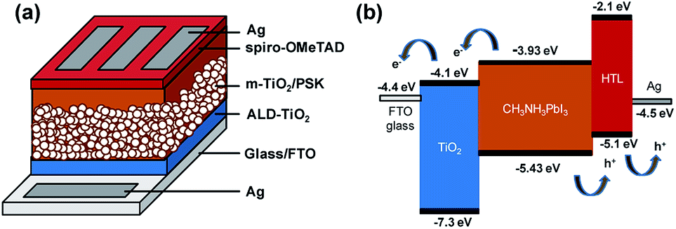 | ||
| Fig. 1 (a) Configuration of the PSC: glass/FTO/ALD-TiO2/m-TiO2/MAPbI3/spiro-OMeTAD/Ag. (b) Diagram of energy levels of each layer of the PSC. | ||
To confirm the structure of the cells layer by layer and the thicknesses of the prepared ALD-TiO2 films, we characterized the cross-sections using a field-emission scanning electron microscope (FESEM). Fig. 2a–f present images of the cross-section of a full PSC using ALD-TiO2 as HBL with thickness 10, 50, 100, 200, 300 and 400 nm, respectively. The thickness of the whole PSK layer is controlled to about 330 nm with a ∼230 nm thick layer of mesoporous TiO2 (m-TiO2) and a PSK layer of thickness ∼100 nm. On top of the PSK layer, we deposited an organic HTL (spiro-OMeTAD) followed by a silver contact electrode of thickness ∼150 nm. All images show a satisfactory contact between each layer that facilitates the charge migration in their paths, which improves the PCE of the cells as the results show below. Both the compact TiO2 and the mesoporous layers play an important role in the extraction of the interfacial charge because of the large surface area and the influence of the satisfactory morphology which facilitate efficient charge extraction and prevent direct contact of the hole with the FTO substrate.
 | ||
Fig. 2 Cross-section SEM of the PSCs with ALD-TiO2 as HBL of thickness (a) 10, (b) 50, (c) 100, (d) 200, (e) 300 and (f) 400 nm. The magnification is ×20![[thin space (1/6-em)]](https://www.rsc.org/images/entities/char_2009.gif) 000; the scale bar is 200 nm for all SEM images. 000; the scale bar is 200 nm for all SEM images. | ||
Fig. 3a and b show the J–V characteristics and the corresponding spectra of the efficiency of conversion of incident photons to current (IPCE), respectively. The improved PCE in Fig. 3a is attributed to the increased short-circuit current (Jsc) and fill factor (FF) for the effective extraction of interfacial charge with the thickness of the ALD-TiO2 layer varied from 10 nm to 200 nm. When the ALD-TiO2 film was thicker than 200 nm, the decreased conductivity in those ALD-TiO2 devices deteriorated the performance, as revealed by decreased Jsc and FF for the devices with ALD-TiO2 of thicknesses 300 and 400 nm as discussed below. The open-circuit voltages (Voc) of all ALD-TiO2 devices appeared to be nearly constant, which confirms that a variation of the film thickness produces no leakage of electrons and holes. The ALD-TiO2 devices exhibit only a small effect of hysteresis for all thicknesses of the ALD-TiO2 compact layer (Fig. 3a). The scan range with varied initial bias plays an important role in the hysteretic behavior and can alter the PV performance.8 A forward scan with a negative starting bias would deteriorate the efficiency, whereas a reverse scan starting with a positive applied bias would increase the performance.37 For each device, the lack of noticeable difference in Jsc observed in Fig. 3a is due to the fact that a given voltage-settling interval is too short to distinguish the small difference in capacitive current.38,39 The PSK film is thin in this work; a thicker PSK layer generally has more defects, which might cause a more serious charge accumulation and a more explicit hysteresis effect. Table 1 summarizes the photovoltaic parameters Jsc, Voc, FF and PCE of the ALD-TiO2-based PSC devices.
 | ||
| Fig. 3 (a) J–V curves, (b) IPCE and integrated current density of ALD-TiO2 with thickness 10, 50, 100, 200, 300 and 400 nm, respectively, as a compact HBL for the best PSC. | ||
| Devices with ALD-TiO2a | J sc/mA cm−2 | V oc/V | FF | PCEb/% | |
|---|---|---|---|---|---|
| a The devices were fabricated using compact ALD-TiO2 HBL materials of varied thickness prepared via ALD. b The average values shown in parentheses were obtained from 15 devices fabricated under the same experimental conditions for each thickness. | |||||
| 10 nm | Reverse scan | 16.90 | 1.00 | 0.565 | 9.55 (9.33 ± 0.14) |
| Forward scan | 16.74 | 1.02 | 0.557 | 9.51 | |
| 50 nm | Reverse scan | 17.44 | 1.00 | 0.599 | 10.45 (9.76 ± 0.33) |
| Forward scan | 17.57 | 1.00 | 0.618 | 10.85 | |
| 100 nm | Reverse scan | 18.63 | 1.01 | 0.689 | 12.97 (12.78 ± 0.19) |
| Forward scan | 18.96 | 1.02 | 0.685 | 13.25 | |
| 200 nm | Reverse scan | 20.81 | 1.03 | 0.702 | 15.03 (14.37 ± 0.44) |
| Forward scan | 21.00 | 1.02 | 0.719 | 15.41 | |
| 300 nm | Reverse scan | 11.46 | 1.03 | 0.693 | 8.18 (7.68 ± 0.23) |
| Forward scan | 11.45 | 1.02 | 0.681 | 7.96 | |
| 400 nm | Reverse scan | 10.02 | 1.03 | 0.509 | 5.25 (4.81 ± 0.17) |
| Forward scan | 10.01 | 1.02 | 0.556 | 5.68 | |
According to the IPCE spectra in Fig. 3b, the best device showed an excellent photocurrent response from 400 to 800 nm, with a maximum IPCE of ∼80%. Fig. 3b also shows that integrating the IPCE over the AM1.5 solar spectrum at irradiance 100 mW cm−2 gives Jsc estimated to be 14.8, 15.1, 16.6, 18.1, 10.8 and 9.3 mA cm−2 for ALD-TiO2 devices of thickness 10, 50, 100, 200, 300 and 400 nm, respectively. Under the solar simulator for these cells, Jsc was measured to be 16.9, 17.4, 18.6, 20.8, 11.5 and 10.1 mA cm−2, respectively. The differences between the current estimated from the IPCE integration and the J–V measurements are within the experimental uncertainties. We also note that we tested these cells in air without encapsulation: there is typically a slightly degraded performance for these PSCs following testing.40
To understand the influence of TiO2 HBL coverage on the device performance, we studied the morphologies of the samples with an atomic-force microscope (AFM). The surface topographies of the ALD-TiO2 compact layer of thickness 10, 50, 100, 200, 300 and 400 nm on FTO so determined are shown in Fig. 4a–g. The root-mean-square roughness (Rrms) of bare FTO was 11.8 nm; Rrms was 16.3, 20.4, 29.6, 33.9, 25.1, and 22.4 nm for ALD-TiO2 thickness 10, 50, 100, 200, 300, and 400 nm, respectively. The surface roughness of every ALD-TiO2 film was thus slightly more rugged than that of the bare FTO substrate and increased with the thickness of the TiO2 film until 200 nm before decreasing again for 300 and 400 nm. The top-view images of FESEM of the TiO2 film also indicate that the grain size of TiO2 reaches the maximum when the TiO2 film thickness is 200 nm (Fig. S2†). This phenomenon can be explained in what follows. At first, nucleation of crystals occurred on the surface of FTO. After that, the crystal grains were propagated and the film roughness increased. After the roughness reached the maximum at the film thickness of 200 nm, the filling of the rugged surface with TiO2 nanoparticles in another layer is supposed to decrease the surface roughness. Although the rough surface is reported to affect the scattering and transmittance between HBL and PSK,41 the results of finite-difference time-domain (FDTD) simulation indicate that the difference of Rrms from 10 to 40 nm scarcely affects the absorption, as shown in Fig. S3.†
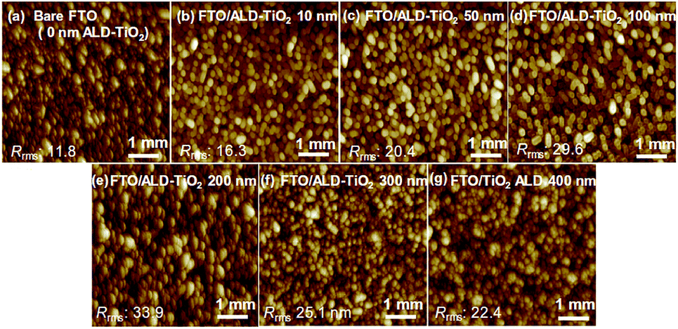 | ||
| Fig. 4 AFM of (a) bare FTO, (b) FTO/ALD-TiO2 10 nm, (c) FTO/ALD-TiO2 50 nm, (d) FTO/ALD-TiO2 100 nm, (e) FTO/ALD-TiO2 200 nm, (f) FTO/ALD-TiO2 300 nm, (g) FTO/ALD-TiO2 400 nm. The magnification is ×12500; the scale bar is 1 μm for all AFM images. | ||
The crystal structures of ALD-TiO2, MAPbI3 and MAPbI3 on ALD-TiO2 of thickness 200 nm were verified with X-ray diffraction (XRD) analysis on the FTO substrate (as shown in Fig. S4a†). The signals obtained for TiO2 marked “*” confirm the formation of the anatase phase. Fig. S4† also shows the XRD investigations of MAPbI3 films deposited on FTO and on ALD-TiO2. The XRD signals of MAPbI3 films were recorded to confirm the PSK tetragonal phase, pointing to the fully formed PSK structure from CH3NH3I and PbI2.42 No impurity signals were detected, indicating that the grown MAPbI3 crystal structures were highly pure and adequately crystalline.
Analysis of the bare FTO and FTO covered with ALD-TiO2 (200 nm) with a FESEM is shown in Fig. S4b and c.† The satisfactory homogeneity with a small grain structure enhanced the surface area of the under-layer and improved the net efficiency of the cells. The top image of MAPbI3 on the ALD-TiO2 layer was obtained using a FESEM as shown in Fig. S4d.† The PSK films were produced with the anti-solvent deposition technique with the addition of chlorobenzene through rapid-deposition crystallization (RDC), showing homogeneous morphology with large grains. For further confirmation of the formed PSK layer, we investigated the surface roughness using an AFM. Rrms of the MAPbI3 film on ALD-TiO2 was ∼17.9 nm; the AFM images confirm the homogeneity and the large grain boundaries of the obtained film as shown in Fig. S4e.† For additional confirmation of the formation of the ALD-TiO2 HBL and MAPbI3, X-ray photoelectron spectra, both wide and narrow, for MAPbI3 and MAPbI3 on TiO2 films yielded results shown in Fig. S5a–d.† Narrow X-ray photoelectron spectra of Ti 2p1/2 and Ti 2p3/2 for TiO2 and O 1s for O2, and narrow X-ray photoelectron spectra of Pb 4f and I 3d for MAPbI3 and MAPbI3 on TiO2 were recorded. As expected, the sample displayed signals of carbon, nitrogen, iodine and lead, which were confirmed with the core-level intensity, indicating a slight deviation from the stoichiometry of CH3NH3PbI3. We obtained the areas of the X-ray photoelectron spectra of these elements by fitting Gaussian peaks after removing the secondary-electron background, followed by normalization with the corresponding atomic sensitivity factors. The small proportions of nitrogen, carbon, lead and iodine can perhaps be attributed to the deficiency of CH3NH3I and PbI2.43 The binding energies for Pb 4f and with I 3d core levels agreed with Lindblad's results.44 A singlet of the I 3d5/2 core level at binding energy 619.5 eV for both TiO2/CH3NH3PbI3 and FTO/CH3NH3PbI3 samples with spin–orbit splitting 11.5 eV to the I 3d3/2 level was recorded for all samples. The distance of the binding energy between the Pb 4f and the I 3d core planes was equal in all samples.45
The charge-extraction properties were investigated for the as-fabricated PSC devices, based on ALD-TiO2 as compact HBL films using the TCSPC technique for PSK deposited on ALD-TiO2 films of varied thickness. We first measured steady-state PL to assess the effect of PL quenching of PSK due to the varied thickness of the ALD-TiO2 films. As the PL spectra show in Fig. 5a, the PL intensities of PSK decreased significantly when the PSK layer was in contact with the ALD-TiO2 compact layer of varied thickness. The PL intensities exhibited the order 400 nm > 300 nm > 10 nm > 50 nm > 100 nm > 200 nm, indicating an electron-extracting ability in the reverse order, i.e., the 200 nm ALD-TiO2 film had the best electron-extracting ability because of the existence of an efficient non-radiative process to quench the PL effectively. To further investigate the kinetics of this efficient non-radiative process, we measured transient PL decays using the TCSPC technique with excitation at 635 nm and probe at 770 nm. The PL transient profiles shown in Fig. 5b are well fitted with a tri-exponential decay function; the fitted time coefficients (τi) for each sample are shown in Table 2 with the corresponding relative amplitudes (Ai) shown in parentheses. The average PL lifetimes (τPL) were determined with an intensity-averaged approach reported elsewhere.46τPL for only MAPbI3 deposited on FTO was determined to be 136 ns, but decreased to 67, 31, 31, 26, 74 and 85 ns when PSK was in contact with the ALD-TiO2 compact layer of thickness 10, 50, 100, 200, 300 and 400 nm, respectively. If we suppose that electron extraction by the ALD-TiO2 compact layer is the predominant path of non-radiative relaxation, the rates of interfacial electron transfer (1/τe) in the MAPbI3/ALD-TiO2 interface are estimated to be 7.6 × 10⁶, 2.5 × 10⁷, 2.5 × 10⁷, 3.1 × 10⁷, 6.2 × 10⁶ and 4.4 × 10⁶ s−1 for thicknesses 10, 50, 100, 200, 300 and 400 nm of the ALD-TiO2 compact layer, respectively; details of the determination of τPL and τe are summarized in Table 2. We found that the rate of electron transfer increased with increased thickness of the ALD-TiO2 film until 200 nm but decreased significantly for a film thickness greater than 200 nm.
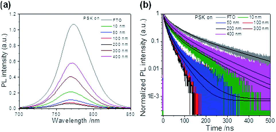 | ||
| Fig. 5 (a) PL spectra and (b) PL decay profiles of PSK, and PSK deposited on varied compact ALD-TiO2 HBL films. The PL spectra were obtained at excitation wavelength 633 nm; the transient PL decays were obtained using TCSPC with excitation at 635 nm and probe at 770 nm. The fitted results are represented in black lines for all results. | ||
| Films | τ 1/ns (A1) | τ 2/ns (A2) | τ 3/ns (A3) | τ PL /ns | 1/τeb/106 s−1 |
|---|---|---|---|---|---|
a The average PL lifetimes were determined according to the following equation,  in which τi and Ai are the fitted time coefficients and the corresponding amplitudes of each component, respectively.
b The interfacial hole-extraction time (τe) at the interface between PSK and HBL was predicted with this equation, in which τi and Ai are the fitted time coefficients and the corresponding amplitudes of each component, respectively.
b The interfacial hole-extraction time (τe) at the interface between PSK and HBL was predicted with this equation, 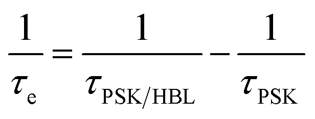 in which τPSK and τPSK/HBL are the PL lifetimes for PSK only and those with PSK deposited on varied compact ALD-TiO2 HBL films, respectively. in which τPSK and τPSK/HBL are the PL lifetimes for PSK only and those with PSK deposited on varied compact ALD-TiO2 HBL films, respectively.
|
|||||
| PSK | 11.7 (0.25) | 51 (0.49) | 187 (0.26) | 135.9 | — |
| PSK/10 nm ALD-TiO2 | 6.2 (0.26) | 26.0 (0.52) | 97.5 (0.22) | 67.0 | 7.6 |
| PSK/50 nm ALD-TiO2 | 4.8 (0.20) | 18.3 (0.64) | 51.5 (0.16) | 30.8 | 25 |
| PSK/100 nm ALD-TiO2 | 4.3 (0.20) | 17.5 (0.65) | 52.5 (0.15) | 30.6 | 25 |
| PSK/200 nm ALD-TiO2 | 1.5 (0.18) | 12.8 (0.60) | 38.3 (0.22) | 25.7 | 31 |
| PSK/300 nm ALD-TiO2 | 5.5 (0.28) | 30.0 (0.50) | 107 (0.22) | 74.3 | 6.2 |
| PSK/400 nm ALD-TiO2 | 4.0 (0.18) | 33.5 (0.54) | 116 (0.28) | 85.3 | 4.4 |
The rough surface might have increased the rate of electron transfer because of the increment of the interfacial area, because a satisfactory relationship between Rrms and 1/τe was observed. Also, because the conductivity of TiO2 might be a problem for a thicker film, we speculate that this anomalous phenomenon might be due to the effect of charge accumulation in the ALD-TiO2/PSK interface that inhibits the interfacial electron transfer on the surface of ALD-TiO2 with film thicknesses 300 and 400 nm. To confirm the relationship between the PL lifetimes of an ALD-TiO2 compact layer, conductivities, and the effect on the device performances, we measured the resistivity of each ALD-TiO2 compact layer with an electrochemical analyzer (ALS/CH Instruments 852C, ALS) and a copper lead wire. The resistivities were measured to be 235, 162, 67, 46, 324 and 1235 Ω cm for thicknesses 10, 50, 100, 200, 300 and 400 nm of the ALD-TiO2 compact layer, respectively; the corresponding conductivities were estimated to be 4.23, 6.17, 14.9, 21.7, 3.09 and 0.81 mS m−1, respectively. Fig. 6 shows a correlation of the PCE with the thickness of the ALD-TiO2 compact layer with respect to the interfacial electron-transfer intervals and the conductivities. The best result was obtained from the sample of ALD-TiO2 with film thickness 200 nm. These results are consistent with the photovoltaic performance in which the ALD-TiO2 device of thickness 200 nm showed the greatest PCE, 15.0%.
 | ||
| Fig. 6 Correlation of device performance (PCE/%) (black) with the thickness of an ALD-TiO2 film with respect to conductivity/S m−1 (red) and rate of interfacial electron transfer (1/τe/s−1) (blue). | ||
ALD is a controllable method to prepare a compact layer with satisfactory reproducibility.47 To assess the reproducibility of the cells, we fabricated 15 devices under the same experimental conditions for each ALD-TiO2 thickness; the corresponding photovoltaic parameters of all devices with averages and standard deviations are summarized in Tables S1–S6.†Fig. 7a shows a histogram to compare the performance distributions of these results with the thickness of ALD-TiO2 films, giving average PCE/% = 9.33 ± 0.14, 9.76 ± 0.33, 12.78 ± 0.19, 14.37 ± 0.44, 7.68 ± 0.23 and 4.81 ± 0.17 for devices made from ALD-TiO2 of thickness 10, 50, 100, 200, 300 and 400 nm, respectively; the histograms for other photovoltaic parameters Jsc, Voc and FF are shown in Fig. S6a–c.† Beyond the efficiency and reproducibility, stability is another important factor for PSC; we thus tested the stability of the ALD-TiO2-based devices. The devices were stored in ambient air (humidity ∼50% and temperature ∼25 °C) and dark conditions to test the stability. As shown in Fig. 7b, the devices demonstrated satisfactory stability over a period of ∼500 h. The results indicate that the efficiency of each device remained stable and maintained ∼96% of its initial value until 200 h and then the efficiency decreased substantially to ∼50% after storage for 500 h.
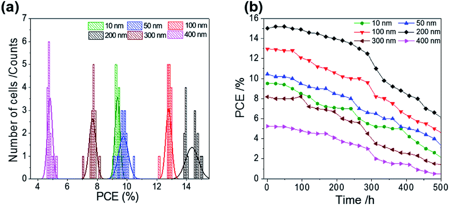 | ||
| Fig. 7 (a) PCE distribution histogram; (b) PCE evolution of 15 devices stored in ambient air for varied duration/h for ALD-TiO2 of thickness 10, 50, 100, 200, 300 and 400 nm, respectively, as a compact HBL. | ||
The photovoltaic performance of a PSC is related to many factors, such as film morphology, surface roughness, carrier lifetime and charge-transport properties. Using ALD-TiO2 as HBL is an effective strategy to have the above-mentioned characteristics under sufficient control, which is critical to achieve high performance comparable with that of other HBLs studied elsewhere.48
Conclusions
We demonstrated that the morphology and thickness of the ALD-TiO2 film as a compact layer play a crucial role in attaining a satisfactory device performance and decreased hysteresis for PSC with a n-i-p configuration. The compact layer designed by ALD is dense, uniform and homogeneous, which ensures only minor defects and maximum contact areas at the interfaces with the PSK/TiO2 layers; it thus enhances charge separation at the PSK/TiO2 interface and promotes electron transport through the ALD-TiO2 layer. We investigated the photovoltaic performance of PSC devices made of an ALD-TiO2 compact layer of film thicknesses varied in the range from 10 to 400 nm. The morphology and surface roughness of the ALD-TiO2 films were investigated with a SEM and an AFM; the electron-transfer characteristics were investigated via steady-state PL and transient PL (via TCSPC) spectra. We found a systematic correlation between the device performance and the surface roughness and the conductivity of an ALD-TiO2 film and the rate of electron transfer as a function of the thickness of an ALD-TiO2 film; the best device performance attained PCE 15.0% at thickness 200 nm, at which great surface roughness and rapid electron transfer occurred. The ALD-TiO2-based PSC devices also showed a minor effect of hysteresis with excellent reproducibility and satisfactory stability during storage in air. This work thus provides another alternative to fabricate mesoscopic PSCs using ALD to prepare a well-controlled TiO2 compact layer of a desired thickness.Experimental methods
Preparation of PSK precursor solution
Methyl ammonium iodide (CH3NH3I) was synthesized via the reaction of methylamine (CH3NH2, 21.6 mL, 40 mass% in water, Alfa Aesar) and hydroiodic acid (HI, 30 mL, 57 mass% in water, with hypophosphorous acid H3PO2 1.5%, Alfa Aesar) and stirred at 0 °C for 2 h under a N2 atmosphere, followed by rotary evaporation to remove the solvent. The CH3NH3I powder was washed three times with diethyl ether (99%, anhydrous, ECHO) and dried in a vacuum oven at 50 °C overnight before use. CH3NH3I was synthesized as described elsewhere.49–51 MAPbI3 precursor solutions (concentration 45% by mass) were prepared in N,N-dimethyl formamide (DMF, anhydrous, Aldrich, 1 mL) mixed with powdered CH3NH3I (175 mg) and PbI2 (99%, Aldrich, 507 mg). The solution was stirred at 70 °C for 1 h before use.Fabrication of electrodes and devices
Before ALD, FTO (TEC7, Hartford, USA) was partially removed from the substrate via etching with zinc powder and HCl (2 M) to produce the desired pattern. The patterned FTO substrates were cleaned with ultrasonication for 30 min in a mixture (acetone, soapy water and isopropyl alcohol (IPA), 1:1:1) and then washed with deionized water. Afterwards, the glass was dried with a N2 blower. Dense thin films of titanium dioxide as HBL with varied thickness were deposited onto the FTO substrate using a commercial hot-wall flow-type ALD reactor (SUNALETM R series, Picosun, Finland). The deposition involved alternating exposure of TiCl4 and deionized water vapor at process temperature 300 °C with a precursor carrier and purge gas N2 at pressure 1.6 kPa. The pulse and purge times for the precursors were 0.1 and 4 s, respectively. The rate of deposition of TiO2 on the FTO glass was estimated to be 0.43 Å per cycle. To fabricate uniform, one-side deposited TiO2 films, we attached the FTO glass tightly to a smooth cover glass, which was previously washed with deionized water in an ultrasonic bath for 5 min. After that, a m-TiO2 layer of thickness approximately 200 nm was spin-coated (100 μL, 3000 rpm, 30 s) and annealed at 450 °C for 30 min. The substrates were subsequently exposed to ozone for 18 min via irradiation (excimer lamp PC-01-H, N-Cobo Co.) under an O2 atmosphere to remove the organic residues. The prepared MAPbI3 precursor solution was deposited onto the prepared substrate with spin coating at 5000 rpm for 15 s; a few drops of chlorobenzene (CBZ) as an anti-solvent were dripped onto the substrate during spin coating after a delay (5 s). The MAPbI3-precursor coated substrates were then dried on a hot plate at 100 °C for 10 min. The HTM layer with a solution containing spiro-OMeTAD (125 mg, Lumtec), Li-TFSI (7.8 mg, Aldrich) in acetonitrile (15.6 μL) and 4-tert-butylpyridine (TBP, 22.6 μL) dissolved in chlorobenzene (1 mL) was then deposited via spin coating at 2000 rpm for 30 s. The sample was transferred to a vacuum system (10−6 Torr) in which silver (thickness ∼ 150 nm) was evaporated through a shadow mask to complete the device fabrication; the active area of the Ag electrodes in the fabricated device was 0.09 cm2.
Characterization of materials and devices
Acknowledgements
We thank Mr Hau-Shiang Shiu for his assistance in SEM measurements. KAKENHI grant No. JP23225006, JP15H00856, JP15K17438, JP15H01073, JP15K04589, JP17H01041, and JP15K20833, Nanotechnology Platform (Hokkaido University) and Dynamic Alliance for Open Innovation Bridging Human, Environment and Materials (Five-Star Alliance) of MEXT, Taiwan Ministry of Science and Technology (contracts MOST 105-2119-M-009-011-MY3 and MOST 104-2119-M-009-001) supported this research. AES thanks National Chiao Tung University (Hsinchu, Taiwan) and Hokkaido University (Sapporo, Japan) for support of his visit to NCTU through the Elite Internship Program agreement between the two universities.References
- A. Kojima, K. Teshima, Y. Shirai and T. Miyasaka, J. Am. Chem. Soc., 2009, 131, 6050–6051 CrossRef CAS PubMed.
- M. M. Lee, J. Teuscher, T. Miyasaka, T. N. Murakami and H. J. Snaith, Science, 2012, 338, 643–647 CrossRef CAS PubMed.
- W. S. Yang, J. H. Noh, N. J. Jeon, Y. C. Kim, S. Ryu, J. Seo and S. I. Seok, Science, 2015, 348, 1234–1237 CrossRef CAS PubMed.
- Y. Zhao and K. Zhu, J. Phys. Chem. Lett., 2014, 5, 4175–4186 CrossRef CAS PubMed.
- J. Xiao, J. J. Shi, D. M. Li and Q. B. Meng, Sci. China: Chem., 2015, 58, 221–238 CrossRef CAS.
- S. D. Stranks, G. E. Eperon, G. Giulia, C. Menelaou, M. J. P. Alcocer, T. Leijtens, L. M. Herz, A. Petrozza and H. J. Snaith, Science, 2013, 342, 341–344 CrossRef CAS PubMed.
- L. Etgar, P. Gao, Z. Xue, Q. Peng, A. K. Chandiran, B. Liu, M. K. Nazeeruddin and M. Grätzel, J. Am. Chem. Soc., 2012, 134, 17396–17399 CrossRef CAS PubMed.
- J. Wei, Y. Zhao, H. Li, G. Li, J. Pan, D. Xu, Q. Zhao and D. Yu, J. Phys. Chem. Lett., 2014, 5, 3937–3945 CrossRef CAS PubMed.
- J. M. Frost, K. T. Butler and A. Walsh, APL Mater., 2014, 2, 081506 CrossRef.
- H.-W. Chen, N. Sakai, M. Ikegami and T. Miyasaka, J. Phys. Chem. Lett., 2015, 6, 164–169 CrossRef CAS PubMed.
- Y. Zhao, C. Liang, H. Zhang, D. Li, D. Tian, G. Li, X. Jing, W. Zhang, W. Xiao, Q. Liu, F. Zhang and Z. He, Energy Environ. Sci., 2015, 8, 1256–1260 CAS.
- S. van Reenen, H. J. Snaith and M. Kemerink, J. Phys. Chem. Lett., 2015, 6, 3808–3814 CrossRef CAS PubMed.
- J. J. Shi, X. Xu, H. Y. Zhang, Y. H. Luo, D. M. Li and Q. B. Meng, Appl. Phys. Lett., 2015, 107, 163901 CrossRef.
- H. Yu, H. Lu, F. Xie, S. Zhou and N. Zhao, Adv. Funct. Mater., 2016, 26, 1411–1419 CrossRef CAS.
- J. M. Azpiroz, E. Mosconi, J. Bisquert and F. De Angelis, Energy Environ. Sci., 2015, 8, 2118–2127 CAS.
- E. L. Unger, E. T. Hoke, C. D. Bailie, W. H. Nguyen, A. R. Bowring, T. Heumuller, M. G. Christoforo and M. D. McGehee, Energy Environ. Sci., 2014, 7, 3690–3698 CAS.
- O. Almora, C. Aranda, I. Zarazua, A. Guerrero and G. G. Belmonte, ACS Energy Lett., 2016, 1, 209–215 CrossRef CAS.
- W. Ke, G. Fang, H. Lei, P. Qin, H. Tao, W. Zeng, J. Wang and X. Zhao, J. Power Sources, 2014, 248, 809–815 CrossRef CAS.
- P. J. Cameron and L. M. Peter, J. Phys. Chem. B, 2003, 107, 14394–14400 CrossRef CAS.
- L. Kavan, N. Tetreault, T. Moehl and M. Grätzel, J. Phys. Chem. C, 2014, 118, 16408–16418 CAS.
- L. Kavan, B. O'Regan, A. Kay and M. Grätzel, J. Electroanal. Chem., 1993, 346, 291–307 CrossRef CAS.
- J. Xia, N. Masaki, K. Jiang and S. Yanagida, J. Phys. Chem. B, 2006, 110, 25222–25228 CrossRef CAS PubMed.
- W. Ke, G. Fang, J. Wang, P. Qin, H. Tao, H. Lei, Q. Liu, X. Dai and X. Zhao, ACS Appl. Mater. Interfaces, 2014, 6, 15959–15965 CAS.
- B. Conings, L. Baeten, T. Jacobs, R. Dera, J. D'Haen, J. Manca and H. G. Boyen, APL Mater., 2014, 2, 081505 CrossRef.
- A. K. Chandiran, A. Yella, M. T. Mayer, P. Gao, M. K. Nazeeruddin and M. Grätzel, Adv. Mater., 2014, 26, 4309–4312 CrossRef CAS PubMed.
- S. Chavhan, O. Miguel, H. J. Grande, V. Gonzalez-Pedro, R. S. Sanchez, E. M. Barea, I. Mora-Sero and R. Tena-Zaera, J. Mater. Chem. A, 2014, 2, 12754–12760 CAS.
- S. M. George, Chem. Rev., 2009, 110, 111–131 CrossRef PubMed.
- X. Shi, K. Ueno, T. Oshikiri and H. Misawa, J. Phys. Chem. C, 2013, 117, 24733–24739 CAS.
- K. Nakamura, T. Oshikiri, K. Ueno, Y. Wang, Y. Kamata, Y. Kotake and H. Misawa, J. Phys. Chem. Lett., 2016, 7, 1004–1009 CrossRef CAS PubMed.
- Y. Wu, X. Yang, H. Chen, K. Zhang, C. Qin, J. Liu, W. Peng, A. Islam, E. Bi, F. Ye, M. Yin, P. Zheng and L. Han, Appl. Phys. Express, 2014, 7, 052301 CrossRef.
- A. Gao, S. Yang, L. Lei, S. Zhang, Q. Cao, J. Xie, J. Li and Y. Liu, Chem. Lett., 2015, 44, 624–626 CrossRef.
- L. Chen, J. R. Wang, L. Q. Xie, C. Zhan, Z. Qin, J. Z. Zhou, J. W. Yan, B. W. Mao and Z. Q. Tian, Electrochem. Commun., 2016, 68, 40–44 CrossRef CAS.
- A. R. b. M. Yusoff and M. K. Nazeeruddin, J. Phys. Chem. Lett., 2016, 7, 851–866 CrossRef CAS PubMed.
- J. H. Heo, H. J. Han, D. Kim, T. K. Ahn and S. H. Im, Energy Environ. Sci., 2015, 8, 1602–1608 CAS.
- X. Xu, H. Zhang, J. Shi, J. Dong, Y. Luo, D. Li and Q. Meng, J. Mater. Chem. A, 2015, 3, 19288–19293 CAS.
- M. Xiao, F. Huang, W. Huang, Y. Dkhissi, Y. Zhu, J. Etheridge, A. Gray-Weale, U. Bach, Y.-B. Cheng and L. Spiccia, Angew. Chem., Int. Ed., 2014, 53, 9898–9903 CrossRef CAS PubMed.
- B. Chen, X. J. Zheng, M. J. Yang, Y. Zhou, S. Kundu, J. Shi, K. Zhu and S. Priya, Nano Energy, 2015, 13, 582–591 CrossRef CAS.
- H.-S. Kim, I.-H. Jang, N. Ahn, M. Choi, A. Guerrero, J. Bisquert and N.-G. Park, J. Phys. Chem. Lett., 2015, 6, 4633–4639 CrossRef CAS PubMed.
- B. Chen, M. Yang, S. Priya and K. Zhu, J. Phys. Chem. Lett., 2016, 7, 905–917 CrossRef CAS PubMed.
- O. Malinkiewicz, C. Roldan-Carmona, A. Soriano, E. Bandiello, L. Camacho, M. K. Nazeeruddin and H. J. Bolink, Adv. Energy Mater., 2014, 4, 1400345 CrossRef.
- H. Hu, B. Dong, H. Hu, F. Chen, M. Kong, Q. Zhang, T. Luo, L. Zhao, Z. Guo, J. Li, Z. Xu, S. Wang, D. Eder and L. Wan, ACS Appl. Mater. Interfaces, 2016, 8, 17999–18007 CAS.
- K. Liang, D. B. Mitzi and M. T. Prikas, Chem. Mater., 1998, 10, 403–411 CrossRef CAS.
- X. Liu, C. Wang, L. Lyu, C. Wang, Z. Xiao, C. Bi, J. Huang and Y. Gao, Phys. Chem. Chem. Phys., 2015, 17, 896–902 RSC.
- R. Lindblad, D. Bi, B. Park, J. Oscarsson, M. Gorgoi, H. Siegbahn, M. Odelius, E. M. J. Johansson and H. Rensmo, J. Phys. Chem. Lett., 2014, 5, 648–653 CrossRef CAS PubMed.
- N. J. Jeon, J. H. Noh, Y. C. Kim, W. S. Yang, S. Ryu and S. I. Seok, Nat. Mater., 2014, 13, 897–903 CrossRef CAS PubMed.
- B. Valeur, in Encyclopedia of Applied Physics, Wiley-Vch, 2009 Search PubMed.
- L. Chen, J.-R. Wang, L.-Q. Xie, C. Zhan, Z. Qiu, J.-Z. Zhou, J.-W. Yan, B.-W. Mao and Z.-Q. Tian, Electrochem. Commun., 2016, 68, 40–44 CrossRef CAS.
- S. Duenas, H. Castan, H. Garcia, E. San Andres, M. Toledano-Luque, I. Martil, G. Gonzalez-Diaz, K. Kukli, T. Uustare and J. Aarik, Semicond. Sci. Technol., 2005, 20, 1044–1051 CrossRef CAS.
- K. C. Wang, J. Y. Jeng, P. S. Shen, Y. C. Chang, E. W. Diau, C. H. Tsai, T. Y. Chao, H. C. Hsu, P. Y. Lin, P. Chen, T. F. Guo and T. C. Wen, Sci. Rep., 2014, 4, 4756 CrossRef PubMed.
- C.-Y. Chan, Y. Wang, G.-W. Wu and E. W.-G. Diau, J. Mater. Chem. A, 2016, 4, 3872–3878 CAS.
- C.-C. Chung, C. S. Lee, E. Jokar, J. H. Kim and E. W.-G. Diau, J. Phys. Chem. C, 2016, 120, 9619–9627 CAS.
Footnote |
| † Electronic supplementary information (ESI) available. See DOI: 10.1039/c7se00220c |
| This journal is © The Royal Society of Chemistry 2017 |