
Neutral-colored semitransparent solar cells based on pseudohalide (SCN−)-doped perovskite†
Si
Chen‡
a,
Buxin
Chen‡
a,
Xue
Gao
a,
Bin
Dong
a,
Hsienwei
Hu
a,
Kai
Yan
a,
Wen
Wen
a and
Dechun
Zou
 *ab
*ab
aBeijing National Laboratory for Molecular Sciences, Key Laboratory of Polymer Chemistry and Physics of Ministry of Education, Center for Soft Matter Science and Engineering, College of Chemistry and Molecular Engineering, Peking University, Beijing 100871, China. E-mail: dczou@pku.edu.cn; Fax: +86-10-6275-9799; Tel: +86-10-6275-9799
bBeijing Engineering Research Center for Active Matrix Display, Peking University, Beijing 100871, China
First published on 19th April 2017
Abstract
A novel strategy that uses SCN− is introduced to develop neutral-colored, semitransparent perovskite film of discrete islands. Micro-structured arrays of perovskite precursor “islands” are formed from the (SCN−)-doped precursor solution by the spin-coating method and demonstrates the maximum AVT of 50% with a device efficiency of 2.4%.
Organic and inorganic hybrid perovskite materials (such as CH3NH3PbI3, CH3NH3PbI3−xClx) are considered the best photovoltaic materials because of their optimal band gaps, high absorption coefficients, and long carrier diffusion lengths.1–3 Organic and inorganic hybrid perovskite materials are also attracting increased attention because they can be fabricated into efficient solar cells through a solution process at low temperatures. Perovskite solar cells with increased efficiency of up to 20% (ref. 4–7) have broad-ranging applications in photovoltaics, especially in building-integrated photovoltaics (BIPVs). Given their strong visible-light absorption, solar cells are installed on roofs, facades, and other parts of buildings without affecting indoor lighting. Most modern buildings have glass walls, thereby substantially increasing the proportion of windows in building surfaces. Consequently, the development of semitransparent perovskite solar cells with no serious impact on the exterior lighting of buildings that can be placed on glass surfaces can greatly expand the range of their applications.
In perovskite solar cells, counter electrodes and perovskite layers have significant effects on the overall light transmission of cells. In recent studies on semitransparent perovskite solar cells, ultra-thin metallic electrodes (Au,8 Ag,9,10etc.), transparent conductive polymers (such as PEDOT)11 and carbon materials (carbon nano-tubes12 and graphene13) have been commonly used as transparent electrodes to reduce the visible-light reflectance and absorption of the electrodes. Perovskite is a material for the photoelectric conversion in perovskite solar cells; thus, visible-light absorption directly affects the output power of the cells. Therefore, the key to prepare the semitransparent perovskite solar cells is to produce photovoltaic cells with weaker visible-light absorption and certain photoelectric conversion efficiencies by determining the visible-light reflectance and absorption balance of perovskite based on the Beer–Lambert law:  , where A is the measured absorbance, a(λ) is the wavelength-dependent absorptivity coefficient, b is the path length, and c is the analyte concentration. By reducing the film thickness of perovskite, the absorbance of the perovskite film can be effectively reduced; thus, this approach is a common strategy for preparing semitransparent perovskite solar cells.11,14–17 By reducing the film thickness of perovskite and the transparent counter electrode, the average visible transmittance (AVT) of the full device can be increased to 40–50% (380–740 nm, as calculated). However, given the nature of the density of states in the conduction and valence bands of the perovskite semiconductor, perovskite more intensely absorbs light rays with wavelengths less than 600 nm; the transmitted light of the semitransparent cells turns red-brown after reducing the film thickness of perovskite.16 This effect is obviously highly detrimental to applications of semitransparent perovskite solar cells in the BIPVs. In addition to reducing the film thickness of perovskite, another strategy to enhance the transmittance of the cells is to lower the perovskite coverage and to prepare an island-like non-continuous perovskite film.8,18,19 The light will pass through any part not covered with perovskite, thereby greatly increasing the short-wavelength light transmittance of the cells, reducing the light transmittance of different wavelengths, and producing neutral-colored semitransparent perovskite solar cells. Based on the strategy, Eperon et al.8 developed a perovskite precursor film with microstrutured architecture by spin-coating a precursor with a molar excess of organic and halide components. The holes in the perovskite precursor film gradually expanded with the volatilization of organic components during the annealing process and finally interconnected, thereby producing a film of discrete islands.8 Thereafter, higher efficiencies are achieved by replacing methylammonium lead iodide perovskite with formamidinium lead iodide. With the volatilization of organic iodides, the island-like perovskite made from the continuous perovskite precursor film limits the further reduction of perovskite coverage, and the AVT of the cells is basically maintained at ∼30%.19 Aharon et al.18 fabricated perovskite grids with a unique wet deposition technique to develop semitransparent perovskite solar cells. By changing the solution concentration and the mesh openings of the printing screen, the coverage of perovskite can be effectively regulated, thereby developing semitransparent cells with AVT up to 67%; however, the perovskite film made with this method is more defective and has lower cell efficiency than the films produced by conventional spin coating methods.18
In this paper, a novel strategy that uses SCN− in the perovskite film is introduced to develop the film of discrete islands. Micro-structured arrays of perovskite precursor “islands” are formed from the (SCN−)-doped perovskite precursor solution by the spin-coating method. By annealing with the precursor film, the organic iodides are volatilized, thereby forming a perovskite crystal and finally developing a film of discrete islands with low coverage. Given the low coverage of perovskite, visible light can be fully transmitted through the uncovered part, with the perovskite film becoming neutral colored while the semitransparent perovskite solar cells are developed, with ultra-thin Ag electrodes as the counter electrodes. This paper demonstrates that the maximum AVT of 50% with an efficiency of 2.4% is the best-reported combination of efficiency and transparency to date. The prepared cells have very broad prospective applications in the field of BIPVs.
The discrete islands are developed with the solution process as shown in Fig. 1a. Pb(SCN)2 and CH3NH3I with a mass ratio of 1![[thin space (1/6-em)]](https://www.rsc.org/images/entities/char_2009.gif) :3 are dissolved in DMF to produce a solution with the mass fraction of 40%. This solution is dropped onto the FTO substrate surface with a dense layer of titanium dioxide, and a (SCN−)-doped perovskite precursor film is formed by spin coating for 30 s at 2000 rpm to develop the film of discrete islands after annealing at 100 °C for 60 min. Fig. 1b shows the morphological changes of the film after annealing at 100 °C. Unlike the findings of Eperon et al., the (SCN−)-doped perovskite precursor film is island-like before annealing, whereas the common perovskite precursor film has a continuous planar structure. As seen from Fig. S1,† the excessive CH3NH3I component is gradually volatilized from the perovskite precursor film as the annealing time is extended, thereby reducing the driving force of the surface energy, gradually leading to morphological changes of the precursor film surface, and finally forming discrete island-like structures. Based on the discrete islands, semitransparent perovskite solar cells are fabricated with spiro-OMeTAD as the hole-transport material and an Ag film (9 nm) as the transparent counter electrode; the schematic is shown in Fig. 1c. The SEM micrograph of the inclined section of the cells (Fig. 1d) shows that perovskite is clearly island-like, and the surface of the island-like perovskite structure is fully covered with spiro-OMeTAD, thereby preventing the direct contact between the counter electrode and perovskite, as well as effectively reducing the number of electrons recombined with holes.
:3 are dissolved in DMF to produce a solution with the mass fraction of 40%. This solution is dropped onto the FTO substrate surface with a dense layer of titanium dioxide, and a (SCN−)-doped perovskite precursor film is formed by spin coating for 30 s at 2000 rpm to develop the film of discrete islands after annealing at 100 °C for 60 min. Fig. 1b shows the morphological changes of the film after annealing at 100 °C. Unlike the findings of Eperon et al., the (SCN−)-doped perovskite precursor film is island-like before annealing, whereas the common perovskite precursor film has a continuous planar structure. As seen from Fig. S1,† the excessive CH3NH3I component is gradually volatilized from the perovskite precursor film as the annealing time is extended, thereby reducing the driving force of the surface energy, gradually leading to morphological changes of the precursor film surface, and finally forming discrete island-like structures. Based on the discrete islands, semitransparent perovskite solar cells are fabricated with spiro-OMeTAD as the hole-transport material and an Ag film (9 nm) as the transparent counter electrode; the schematic is shown in Fig. 1c. The SEM micrograph of the inclined section of the cells (Fig. 1d) shows that perovskite is clearly island-like, and the surface of the island-like perovskite structure is fully covered with spiro-OMeTAD, thereby preventing the direct contact between the counter electrode and perovskite, as well as effectively reducing the number of electrons recombined with holes.
 | ||
| Fig. 1 (a) Schematic of the preparation process and formation of the CH3NH3PbI3−x(SCN)x perovskite film; (b) morphological changes of the film after annealing at 100 °C; (c) schematic of the structure of the solar cell with island-like perovskite structures; (d) scanning electron micrograph of a dip plane of the full cell (device structure: FTO/t-TiO2/perovskite/spiro/Ag). | ||
Meanwhile, the crystal structure and elemental distribution of the CH3NH3PbI3−x(SCN)x perovskite film were characterized. The XRD characterization of different films is shown in Fig. 2. Similar to the XRD spectra of the CH3NH3PbI3−xClx or CH3NH3PbI3 crystal structures (Fig. S12†), the CH3NH3PbI3−x(SCN)x structures have apparent diffraction peaks at 14.1°, 28.2°, and 31.9°, which respectively correspond to the three lattice planes of perovskite (namely, planes 110, 220, and 310). Similar to Cl−, doping with SCN− does not appreciably change the crystal structure of perovskite.20–22 In addition, compared with CH3NH3PbI3−xClx, CH3NH3PbI3−x(SCN)x has sharper diffraction peaks, thereby indicating that SCN− can improve the crystallinity within the reduced grain boundaries and the lowered defect density.22,23 To further demonstrate the presence of SCN− in the discrete islands, energy-dispersive X-ray analysis (EDX) was conducted on the CH3NH3PbI3−x(SCN)x perovskite film. Photoelectron spectroscopy (Fig. S2†) was used to analyze the elemental distribution of Pb and I in perovskite and that of S in SCN−. The distribution of the three elements agrees with the SEM micrographs of the island-like structures, thereby verifying the presence of SCN−.
 | ||
| Fig. 2 XRD spectra of the CH3NH3PbI3−x(SCN)x films, CH3NH3PbI3−xClx films, PbCl2, and Pb(SCN)2 (star marks in turn represent the 110, 220, and 310 lattice planes of perovskite). | ||
Furthermore, the effects of SCN− on the morphology and crystallization of the perovskite film are discussed. Based on the composition of the precursor solution (PbCl2:CH3NH3I = 1:3, a DMF solution with the mass fraction of 40%) in the CH3NH3PbI3−xClx system, the effects of different proportions of SCN− in the precursor solution on the perovskite film are analyzed. Pb(SCN)2, PbCl2, and CH3NH3I are added to the precursor solution with a mass ratio of x:(1 − x):3, the perovskite precursor solution of the same mass concentration is prepared respectively with five different proportions: x = 0, x = 0.25, x = 0.5, x = 0.75, and x = 1. After spin coating under the same conditions, the perovskite film is formed by annealing at 100 °C. Fig. S3† shows the morphology of the perovskite film prepared with the precursor solution containing different SCN− contents as visualized by SEM. The figure shows that as the Pb(SCN)2 content in the precursor solution incrementally increases (x gradually increases from 0 to 1), the coverage of the perovskite film decreases, with the morphology changing from the original continuous flat planar structure into the partially covered semi-continuous structure; highly discrete island-like structures are also produced. The XRD characterization (Fig. S4†) of the perovskite film prepared with the precursor solution of different Pb(SCN)2 contents shows that different proportions of Pb(SCN)2 in the precursor solution do not affect the position of the diffraction peak. Thereby indicating that SCN− does not significantly change the crystal structure of perovskite, which is consistent with the previous conclusions.
Subsequently, the light absorption of the transparent perovskite solar cells without the counter electrode was characterized. The physical photograph (Fig. 3a) shows that the prepared semitransparent solar cells have good light transmission. Fig. 3b presents the UV-visible absorption spectra of the perovskite solar cells with CH3NH3PbI3−x(SCN)x and CH3NH3PbI3−xClx as the light-absorbing materials. The CH3NH3PbI3−xClx perovskite film exhibits strong absorption within the entire visible-light region, with 100% absorption of light with wavelengths below 600 nm. The CH3NH3PbI3−x(SCN)x perovskite film is composed of island structures; thus, numerous light rays can pass through the gaps between the island-like structures without being absorbed; the average transmittance of the prepared solar cells within the visible-light region (380–740 nm) can reach 50% (Fig. 3b and S5†). The transmittance spectra as well as optical photograph of full solar cell devices are shown in Fig. S10.† In addition, the cells prepared with CH3NH3PbI3−x(SCN)x perovskite films have flatter spectra of UV-visible absorption, thereby implying that the cells have uniform light absorbance of different wavelengths and the light rays become neutral colored after passing through the semitransparent cells. To further characterize the neutral-colored cells, the color perception indices were calculated with the CIE 1931xy color space (Fig. 3c). The intensity of the transmitted light was obtained from the AM1.5 solar spectra and the UV-visible absorption spectra of the cells. As shown in Fig. 3c, the light transmitted through the solar cells by the CH3NH3PbI3−xClx perovskite film appears clear and red-brown, thereby indicating that the cells have significant differences in their light absorption of different wavelengths. We have also delivered the color perception indices calculation of the full device (Fig. S11†) and indicated that neutral-colored cells are obtained. The light transmitted through the cells with the CH3NH3PbI3−x(SCN)x perovskite film is within the white light region, thereby indicating that the neutral-colored cells can uniformly transmit light of different wavelengths and greatly expand the applications of semitransparent perovskite solar cells.
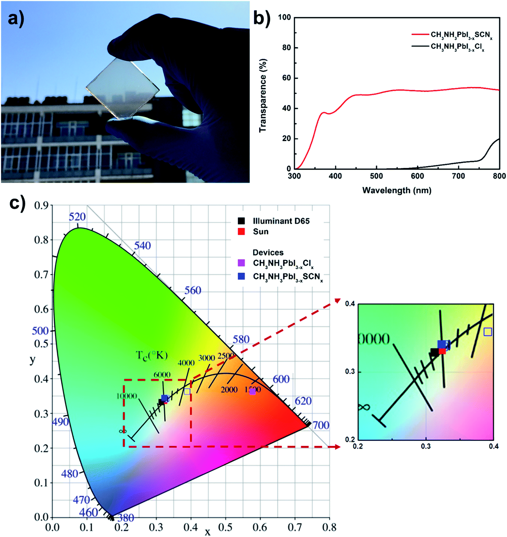 | ||
| Fig. 3 (a) Photographs of the semitransparent device without the counter electrode (device structure: FTO/t-TiO2/perovskite/spiro); (b) UV-visible absorption spectra of devices (device structure: FTO/t-TiO2/perovskite) with CH3NH3PbI3−x(SCN)x and CH3NH3PbI3−xClx as the respective light-absorbing materials; (c) color coordinates of the devices (device structure: FTO/t-TiO2/perovskite) under AM1.5 illumination on the CIE xy 1931 chromaticity diagram and the enlarged central region. | ||
To further explore the transmittance–performance relationships of cells with the CH3NH3PbI3−x(SCN)x perovskite film, a series of cells of different transmittance values are prepared by regulating the ratio of Pb(SCN)2 to PbCl2 in the perovskite precursor solution. Fig. 4a shows the perovskite solar cells with different Pb(SCN)2 contents in the precursor solution. As seen from the figure, when the Pb(SCN)2 content in the precursor solution increases, the cells gradually turn from dark red brown to light gray, whereas the cell transmittance gradually increases. The perovskite coverage, mean visible-light transmittance, and cell efficiency are shown in Table 1. With the higher Pb(SCN)2 content in the precursor solution, the AVT of the cells increases from 1.3% to 50%, whereas the perovskite coverage is reduced from 99.9% to 28.3% (detailed description about methods of obtaining the statistics of perovskite coverage can be found in the experimental part of the ESI†). As seen from the J–V curves of the prepared cells in Fig. 4b, with the higher Pb(SCN)2 content in the precursor solution, the short-circuit current and open-circuit voltage gradually decrease. The cells with the highest transmittance retain the short-circuit current of 6.2 mA cm−2, the open-circuit voltage of 0.68 V, the fill factor of 0.58, the final cell efficiency of up to 2.4%, and the average efficiency of 2.1% (Fig. 4d and S7†). No obvious hysteresis is observed under the optimized device preparation conditions (Fig. S8†). Considering that during practical use solar cells will be heated up by sunlight, we also conduct thermal stability studies of devices (Fig. S13†). To further characterize the photoelectric conversion properties of the cells, the external quantum efficiencies (EQEs) of the two types of perovskite solar cells with CH3NH3PbI3−xClx and CH3NH3PbI3−x(SCN)x are characterized. Compared with solar cells containing the CH3NH3PbI3−xClx perovskite film, the EQE massively declined in the solar cells containing the CH3NH3PbI3−x(SCN)x perovskite film, with the integral short-circuit current dropping from 22 mA cm−2 to 5.8 mA cm−2. These trends are consistent with the previous conclusions that the short-circuit current gradually decreases (Fig. 4c). In addition, the EQE curves of the solar cells containing the CH3NH3PbI3−x(SCN)x perovskite film are flatter, thereby indicating the more uniform light absorption and conversion of different wavelengths, which is consistent with the previous conclusion that the light spectra are transmitted through the cells. Finally, Fig. 4e shows the relationships among the measured short-circuit current density, AVT, and island-like perovskite coverage. As seen from the figure, with the gradual decline of the perovskite coverage, the AVT gradually increased, whereas the short-circuit current density of the cells gradually declined. Therefore, by adding Pb(SCN)2 to the perovskite precursor solution, the coverage of perovskite can be effectively adjusted to regulate the AVT and short-circuit current of the prepared cells, as well as attain a certain trade-off between the cell transmittance and cell efficiency.
 | ||
| Fig. 4 (a) Photograph of devices (device structure: FTO/t-TiO2/perovskite/spiro) prepared with different SCN− contents with the increasing SCN− content solution concentration ratio (PbCl2:Pb(SCN)2:CH3NH3I from left to right: 1:0:3, 0.75:0.25:3, 0.5:0.5:3, 0.25:0.75:3, 0:1:3); (b) J–V curves of the perovskite cells of different transmittance values. Perovskite layers with higher AVT% are prepared with different SCN− contents with the increasing SCN− content solution concentration ratio (PbCl2:Pb(SCN)2:CH3NH3I from left to right: 1:0:3, 0.75:0.25:3, 0.5:0.5:3, 0.25:0.75:3, 0:1:3); (c) EQE spectra of the cells with CH3NH3PbI3−x(SCN)x and CH3NH3PbI3−xClx as light-absorbing materials; (d) relationship among AVT, short-circuit current density, and perovskite coverage; (e) relationship between the current density and AVT of perovskite cells with different coverages; (f) comparison of perovskite cells in the present work with other semitransparent solar cells with island-like perovskite films in terms of transmittance and cell efficiency (the work in the chart corresponds in turn from the above to ref. 8, 18 and 19). | ||
| Solution concentration ratio (PbCl2:Pb(SCN)2:CH3NH3I) |
AVT (%) | V OC (V) | J SC (mA cm−2) | FF | Efficiency (%) | Coverage (%) |
|---|---|---|---|---|---|---|
| 1:0:3 |
1.3 | 0.91 | 21.4 | 0.71 | 13.8 | 99.9 |
| 0.75:0.25:3 |
2.5 | 0.75 | 17.8 | 0.6 | 8.0 | 92.9 |
| 0.5:0.5:3 |
22.8 | 0.67 | 11.2 | 0.58 | 4.4 | 52.1 |
| 0.25:0.75:3 |
37.9 | 0.67 | 8.6 | 0.52 | 3.0 | 36.2 |
| 0:1:3 |
50.0 | 0.68 | 6.2 | 0.58 | 2.4 | 28.3 |
Finally, given the high transmittance when the AVT is 50%, the cell efficiency can still reach 2.4%. This level is optimal for the existing semitransparent perovskite solar cells under the same light transmittance (Fig. 4f and S9†). By adding Pb(SCN)2 to the perovskite precursor solution, perovskite precursor film with island-like structures is obtained; thus, perovskite film with discrete islands and lower coverage is obtained after annealing. The highly discrete island-like perovskite structures ensure good transmittance of the cells and allow light to effectively pass through the gaps, with the uniform absorption of light rays of different wavelengths. Finally, neutral-colored semitransparent perovskite solar cells with high AVT are prepared. More importantly, in addition to the traditional strategy of forming island-like perovskite structures with excessive volatilized organic components, a new strategy is explored, where the highly discrete islands with the micro-structured perovskite film are prepared from discrete perovskite precursor film. The prepared neutral-colored semitransparent perovskite solar cells with high AVT have broad prospective applications in BIPVs, especially in lighting-ISG devices.
Acknowledgements
This study is jointly supported by National Natural Science Foundation of China (No. 51573004) and Beijing Natural Science Foundation (No. Z160002). The authors also want to thank Mr Xiao Yu for the useful discussions and suggestions.References
- H. S. Kim, C. R. Lee, J. H. Im, K. B. Lee, T. Moehl, A. Marchioro, S. J. Moon, R. Humphry-Baker, J. H. Yum, J. E. Moser, M. Gratzel and N. G. Park, Lead Iodide Perovskite Sensitized All-Solid-State Submicron Thin Film Mesoscopic Solar Cell with Efficiency Exceeding 9%, Sci. Rep., 2012, 2, 591 Search PubMed.
- S. D. Stranks, G. E. Eperon, G. Grancini, C. Menelaou, M. J. P. Alcocer, T. Leijtens, L. M. Herz, A. Petrozza and H. J. Snaith, Electron–Hole Diffusion Lengths Exceeding 1 Micrometer in an Organometal Trihalide Perovskite Absorber, Science, 2013, 342(6156), 341–344 CrossRef CAS PubMed.
- G. C. Xing, N. Mathews, S. Y. Sun, S. S. Lim, Y. M. Lam, M. Gratzel, S. Mhaisalkar and T. C. Sum, Long-Range Balanced Electron- and Hole-Transport Lengths in Organic–Inorganic CH3NH3PbI3, Science, 2013, 342(6156), 344–347 CrossRef CAS PubMed.
- A. Kojima, K. Teshima, Y. Shirai and T. Miyasaka, Organometal Halide Perovskites as Visible-Light Sensitizers for Photovoltaic Cells, J. Am. Chem. Soc., 2009, 131(17), 6050–6051 CrossRef CAS PubMed.
- J. Burschka, N. Pellet, S. J. Moon, R. Humphry-Baker, P. Gao, M. K. Nazeeruddin and M. Gratzel, Sequential deposition as a route to high-performance perovskite-sensitized solar cells, Nature, 2013, 499(7458), 316–319 CrossRef CAS PubMed.
- H. P. Zhou, Q. Chen, G. Li, S. Luo, T. B. Song, H. S. Duan, Z. R. Hong, J. B. You, Y. S. Liu and Y. Yang, Interface engineering of highly efficient perovskite solar cells, Science, 2014, 345(6196), 542–546 CrossRef CAS PubMed.
- G. Hodes, Perovskite-Based Solar Cells, Science, 2013, 342(6156), 317–318 CrossRef CAS PubMed.
- G. E. Eperon, V. M. Burlakov, A. Goriely and H. J. Snaith, Neutral Color Semitransparent Microstructured Perovskite Solar Cells, ACS Nano, 2014, 8(1), 591–598 CrossRef CAS PubMed.
- Y. Yang, Q. Chen, Y. T. Hsieh, T. B. Song, N. De Marco, H. P. Zhou and Y. Yang, Multilayer Transparent Top Electrode for Solution Processed Perovskite/Cu(In,Ga) (Se,S)(2) Four Terminal Tandem Solar Cells, ACS Nano, 2015, 9(7), 7714–7721 CrossRef CAS PubMed.
- C. Y. Chang, Y. C. Chang, W. K. Huang, K. T. Lee, A. C. Cho and C. C. Hsu, Enhanced Performance and Stability of Semitransparent Perovskite Solar Cells Using Solution-Processed Thiol-Functionalized Cationic Surfactant as Cathode Buffer Layer, Chem. Mater., 2015, 27(20), 7119–7127 CrossRef CAS.
- L. L. Bu, Z. H. Liu, M. Zhang, W. H. Li, A. L. Zhu, F. S. Cai, Z. X. Zhao and Y. H. Zhou, Semitransparent Fully Air Processed Perovskite Solar Cells, ACS Appl. Mater. Interfaces, 2015, 7(32), 17776–17781 CAS.
- X. Y. Wang, Z. Li, W. J. Xu, S. A. Kulkarni, S. K. Batabyal, S. Zhang, A. Y. Cao and L. H. Wong, TiO2 nanotube arrays based flexible perovskite solar cells with transparent carbon nanotube electrode, Nano Energy, 2015, 11, 728–735 CrossRef CAS.
- P. You, Z. K. Liu, Q. D. Tai, S. H. Liu and F. Yan, Efficient Semitransparent Perovskite Solar Cells with Graphene Electrodes, Adv. Mater., 2015, 27(24), 3632–3638 CrossRef CAS PubMed.
- J. H. Heo, H. J. Han, M. Lee, M. Song, D. H. Kim and S. H. Im, Stable semi-transparent CH3NH3PbI3 planar sandwich solar cells, Energy Environ. Sci., 2015, 8(10), 2922–2927 CAS.
- C. Roldan-Carmona, O. Malinkiewicz, R. Betancur, G. Longo, C. Momblona, F. Jaramillo, L. Camacho and H. J. Bolink, High efficiency single-junction semitransparent perovskite solar cells, Energy Environ. Sci., 2014, 7(9), 2968–2973 CAS.
- C. O. R. Quiroz, L. Levchuk, C. Bronnbauer, M. Salvador, K. Forberich, T. Heumuller, Y. Hou, P. Schweizer, E. Spiecker and C. J. Brabec, Pushing efficiency limits for semitransparent perovskite solar cells, J. Mater. Chem. A, 2015, 3(47), 24071–24081 Search PubMed.
- E. Della Gaspera, Y. Peng, Q. C. Hou, L. Spiccia, U. Bach, J. J. Jasieniak and Y. B. Cheng, Ultra-thin high efficiency semitransparent perovskite solar cells, Nano Energy, 2015, 13, 249–257 CrossRef CAS.
- S. Aharon, M. Layani, B. E. Cohen, E. Shukrun, S. Magdassi and L. Etgar, Self-Assembly of Perovskite for Fabrication of Semitransparent Perovskite Solar Cells, Adv. Mater. Interfaces, 2015, 2(12), 1500118 CrossRef.
- G. E. Eperon, D. Bryant, J. Troughton, S. D. Stranks, M. B. Johnston, T. Watson, D. A. Worsley and H. J. Snaith, Efficient, Neutral-Color Semitransparented Solar Cells Based on Microstructured Formamidinium Lead Trihalide Perovskite, J. Phys. Chem. Lett., 2015, 6(1), 129–138 CrossRef CAS PubMed.
- T. Baikie, Y. N. Fang, J. M. Kadro, M. Schreyer, F. X. Wei, S. G. Mhaisalkar, M. Graetzel and T. J. White, Synthesis and crystal chemistry of the hybrid perovskite (CH3NH3)PbI3 for solid-state sensitised solar cell applications, J. Mater. Chem. A, 2013, 1(18), 5628–5641 CAS.
- Q. Chen, H. P. Zhou, Z. R. Hong, S. Luo, H. S. Duan, H. H. Wang, Y. S. Liu, G. Li and Y. Yang, Planar Heterojunction Perovskite Solar Cells via Vapor-Assisted Solution Process, J. Am. Chem. Soc., 2014, 136(2), 622–625 CrossRef CAS PubMed.
- S. Dharani, H. A. Dewi, R. R. Prabhakar, T. Baikie, C. Shi, Y. H. Du, N. Mathews, P. P. Boix and S. G. Mhaisalkar, Incorporation of Cl into sequentially deposited lead halide perovskite films for highly efficient mesoporous solar cells, Nanoscale, 2014, 6(22), 13854–13860 RSC.
- Z. G. Xiao, Q. F. Dong, C. Bi, Y. C. Shao, Y. B. Yuan and J. S. Huang, Solvent Annealing of Perovskite-Induced Crystal Growth for Photovoltaic-Device Efficiency Enhancement, Adv. Mater., 2014, 26(37), 6503–6509 CrossRef CAS PubMed.
Footnotes |
| † Electronic supplementary information (ESI) available. See DOI: 10.1039/c7se00122c |
| ‡ These authors contributed equally to this work. |
| This journal is © The Royal Society of Chemistry 2017 |