
Novel photoanode architecture for optimal dye-sensitized solar cell performance and its small cell module study
K.
Susmitha
a,
M. Naresh
Kumar
b,
M.
Gurulakshmi
a,
L.
Giribabu
 c and
M.
Raghavender
*a
c and
M.
Raghavender
*a
aDepartment of Physics, Yogi Vemana University, Kadapa-516003, A.P., India. E-mail: toraghavender@rediffmail.com
bTKR College of Engineering, Hyderabad-500097, T.S., India
cInorganic and Physical Chemistry, CSIR-Indian Institute of Chemical Technology, Hyderabad-500007, T.S., India
First published on 24th February 2017
Abstract
The present study demonstrates a novel photoanode for dye-sensitized solar cells (DSSC) that consists of a top active layer (18 nm TiO2 with N719) developed over a scattering layer (200 nm TiO2) to promote improved usage of sunlight for conversion into electricity. Cell (D-2) with this novel photoanode exhibited improved incident photon-to-current-conversion efficiency (IPCE) of 76% and efficiency of 9.61% compared with the standard photoanode D-1 cell, revealing 72% IPCE and 8.72% efficiency. A fraction of transmitting light through the scattering layer strikes dye molecules of the top active layer for generating additional electrons with similar means to the bottom active layer (18 nm TiO2 with N719). A silver grid stripe-type small DSSC module was fabricated with the proposed architecture photoanode with 8.64 cm2 active area that realized a 5.64% efficiency. The present study revealed that the novel architecture photoanode DSSC offers improved power conversion performance and has potential to become an architecture for DSSC applications.
Introduction
Dye-sensitized solar cells (DSSC) are particularly attractive for their high conversion efficiency, low-cost, easy to fabrication,1etc., which drives the technology to supersede silicon photovoltaics. DSSC has reached a 14% efficiency.2 Typically, DSSC consists of three major components: a dye-sensitized photoanode, an electrolyte, and a Pt-deposited counter-electrode used for the catalysis of the iodide/triiodide (I−/I3−) redox system. The photoanode plays a vital role, having an important influence3,4 on the conversion performance due to light harvesting, electron collection, and injection, etc.5,6 The morphology of TiO2 in the photoanode is also important to achieve higher efficiency.7,8 Photoanodes are normally fabricated with TiO2 nanoparticles of about 20–25 nm size, and they remain transparent in the visible region of the solar spectrum. In this case, solar energy is only partially harvested by the active layer. Enhanced light harvest performance of the photoanode is achieved by the light scattering effect, engineering of dyes, etc.9,10 This approach promotes interaction of incident photons with dye molecules and thereby results in more light harvesting. The idea of light scattering is to extend the travel distance by confining light propagation, i.e. adequate light trapping in the device and increasing the absorption path length of photons and optical confinement.5,11,12 This approach promotes interaction of incident photons with dye molecules towards electron release. During the last few years, substantial efforts have been devoted towards exploring new designs13,14 for device fabrication to enhance the device performance. However, a very small fraction of incident photons in the photoanode will diffuse/transmit through the scattering TiO2 layer and will not be used for photovoltaic energy conversion.5 For this reason, we designed a novel photoanode architecture in which an additional top active layer was coated over the scattering TiO2 layer to utilize the transmitting photons for energy conversion (minimize the loss of radiation5). Moreover, we applied a similar concept to a module and developed a photoanode with 8.64 cm2 active area.Results and discussion
One of the ways to enhance light harvest effect of the photoanode is by laying an additional layer on top of the active layer of the photoanode using large-sized nanoparticles. Despite this light-scattering layer, a fraction of light in the photoanode is not used for energy conversion due to diffusion. For this reason, we coated an additional active layer on top of the light-scattering layer to utilize the diffused light of the light-scattering layer. As a result, a large quantity of dye was anchored to the surface of the semiconductor. Dye molecules anchored with the top active layer will absorb photons that release electrons, thereby improving efficiency. The developed photoanode-1, 2, and 3 are illustrated in Fig. 1 (inset a), and their preparation process is described in the experimental section. Photoanode architecture details are given in Table 1. The amount of dye adsorbed onto the TiO2 film depends on the immersion time.15 Herein, the variation of dye adsorption over the TiO2 film with time was studied in the developed photoanodes and is represented in Fig. 1 (inset-b). The developed photoanodes showed a similar pattern with time. For up to 24 h of anchoring time, the absorption reached a maximum value, and afterwards, diminishing behavior was observed. This could be due to more dye molecules attached to the dye monolayer by van der Waals forces, which is known as molecular stacking.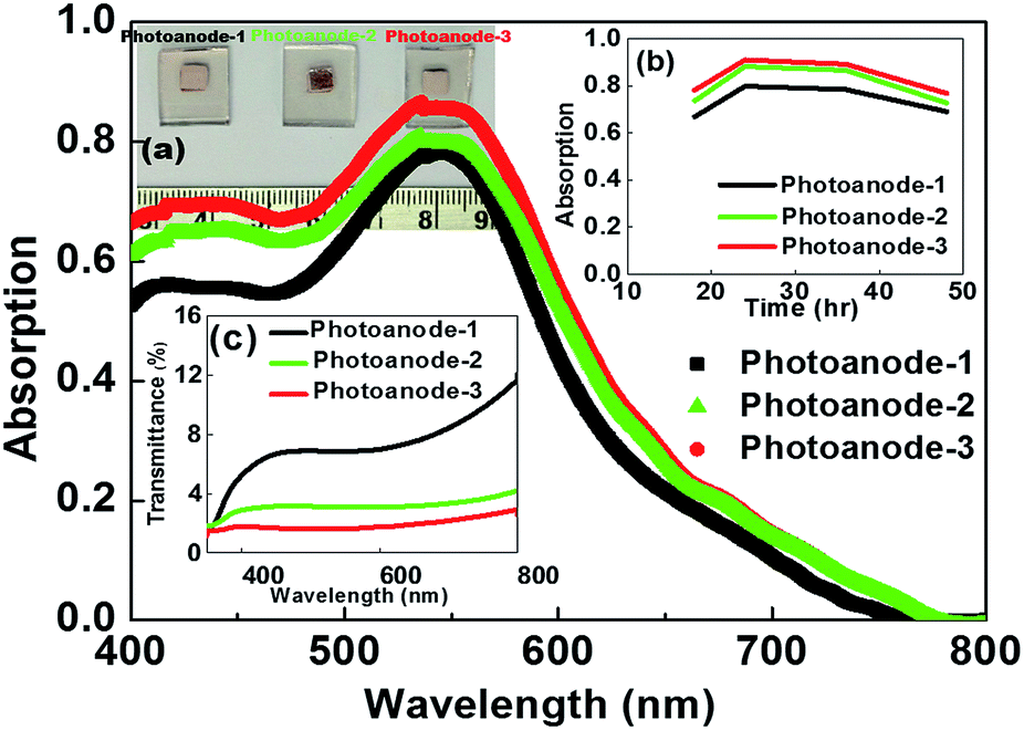 | ||
| Fig. 1 Photoanodes (inset-a) optical absorption, time-dependence adsorption (inset-b), and transmittance (inset-c) spectra. | ||
| Photoanode | Photoanode details | Cell |
|---|---|---|
| Photoanode-1 | FTO/18NR + 18NR + WER2-O | D-1 |
| Photoanode-2 | FTO/18NR + 18NR + WER2-O + 18NR | D-2 |
| Photoanode-3 | FTO/18NR + 18NR + 18NR + WER2-O | D-3 |
Optical absorption spectra of photoanodes soaked for 24 h in N719 dye are presented in Fig. 1. Photoanode-3 had higher absorbance compared with the other photoanodes. Coating of an additional top active layer over the scattering layer may enhance additional Lewis acid sites that leads to increased absorption.16 It was proven that the larger TiO2 scattering layer improved the optical absorption due to an increased optical path length for the incident light.17 The path length/travelling distance of the incident light in photoanodes 2 and 3 was longer and provided additional dye excitations. Transmittance spectra of the photoanodes are illustrated in Fig. 1 (inset c) and the percentage of photoanode-1 transmittance was higher compared to those of photoanodes 2 and 3, indicating loss of light radiation as reported in earlier studies.5 The proposed novel architecture photoanode-2 will address this issue to utilize the loss of light radiation towards energy conversion.
The test cell devices were fabricated using our new active layer concept and a liquid redox electrolyte (I−/I3−). Fig. 2(a) reveals the incident photon-to-conversion efficiency (IPCE) spectra of the test cells using a different photoanode architecture. We observed an IPCE of 76%, 72%, and 70% at ∼550 nm for D-2, D-1, and D-3, respectively, that confirms that the additional top active layer over the scattering layer induced more photogenerated electrons towards energy conversion.
 | ||
| Fig. 2 (a) IPCE and (b) photocurrent density–voltage spectra of D-1, D-2, and D-3 devices. | ||
Fig. 2(b) illustrates the photocurrent density–voltage (J–V) curves of D-1, D-2, and D-3 cells, and the corresponding photovoltaic data are presented in Table 2. Fig. 2(b) demonstrates that the power conversion efficiency (PCE) of D-2 cell was higher than those of the D-1 and D-3 cells. This improved PCE could be due to its enhanced open-circuit voltage (VOC), short-circuit current density (JSC), and fill factor (FF), resulting from the additional top active layer over the scattering layer. The efficiency of the D-2 cell was 9.61%, which is higher than those of D-1 (8.72%) and D-3 (7.40%) cells due to its improved short circuit current density of 23.5 mA cm−2, open circuit voltage of 0.73 V, and fill factor of 0.56. The VOC mainly depends on the number of electrons injected into the TiO2 conduction band; VOC of the D-2 cell was increased may be due to a higher number of electrons injected into TiO2 conduction, as it is evident in the IPCE spectra.18 However, for the D-1 cell, the JSC (22.8 mA cm−2), VOC (0.71 V), and FF (0.52) were lower than those of the D-2 cell, and for the D-3 cell, these were as follows: 0.67 V of VOC, 20.87 mA cm−2 of JSC, FF of 0.51, and a 7.40% efficiency. Note that the efficiency of all the cells mainly resulted from change of JSC and it could be found that the change of the extrema in IPCE was consistent with that of JSC. The efficiency improvement of the D-2 cell was due to the relatively large surface area for effective dye adsorption, coating of the additional top active layer over the scattering layer for increased electron-travelling path and is in good agreement with the IPCE studies. It has been well reported and the present studies observations indicates that improvement in performance is due to additional light back scatter and coating of the additional top active layer involved in energy conversion.19 The conceptual view of transmitting light utilization in DSSC is presented in the Scheme 1 hereinafter.
 | ||
| Scheme 1 Conceptual outlook of the proposed photoanodes. | ||
Electrochemical impedance spectroscopy (EIS) studies were conducted, and Nyquist plots and bode plots are depicted in Fig. 3 and its inset, respectively. The EIS parameters were evaluated by fitting its equivalent circuit model, which is summarized in Table 3. D-2 cell resistances RS (R1), RCT1 (R2), and RCT2 (R3) were lower compared to those of D-1 and D-3, indicating D-2 had a reduced resistance at the TiO2-electrolyte interface and/or Pt-electrolyte interface.
 | ||
| Fig. 3 EIS performance, equivalent circuit of cells, and Bode plots (inset). | ||
| Parameter | D-1 | D-2 | D-3 |
|---|---|---|---|
| R 1 (Ω) | 49.50 | 35.70 | 52.00 |
| R 2 (Ω) (×102) | 31.90 | 19.30 | 75.90 |
| R 3 (Ω) (×102) | 41.80 | 26.00 | 80.70 |
| C 1 (µF) | 4.43 | 8.02 | 4.00 |
| C 2 (µF) | 5.39 | 5.33 | 6.24 |
| W (Ω) | 62.20 | 10.00 | 66.00 |
The semicircle shape in the Nyquist plots is associated with charge transfer across the TiO2/dye/electrolyte interface.20 From Fig. 3, it can be observed that the semicircles diameter increases as D-2 < D-1 < D-3, suggesting a reduction in charge transfer resistance at the TiO2/dye/electrolyte interface,21 which may be due to higher specific surface area, effective dye adsorption, and harvesting light for more active sites of photoanodes contact with electrolyte and more electrons that can transfer from TiO2. The reduction of any resistance of RS, RCT1, and RCT2 provided the decreased total electrical resistance of the cell. The resistance between the TiO2/dye/electrolyte interfaces of the DSSCs fabricated by an additional top active layer over the scattering layer had a lower value (D-2, photoanode-2). For the D-3 cell, the thicker TiO2 film hindered dye absorption and perturbed the transport of photogenerated electrons from TiO2 to the conducting FTO layer. Coating of the additional top active layer in D-2 could adsorb a greater number of dye molecules, and the transmitted light through the scattering layer strikes and excites the dye molecules, thereby releasing more electrons, i.e. causes an increase in the number of photogenerated electrons. These extra released electrons in the top active layer also contributed towards an improved JSC value and in turn enhanced the overall cell efficiency.
DSSC is an environmentally friendly and simple fabrication procedure, with potential for emerging applications such as large area smart windows,22 portable electronic gadgets, etc.23,24 These possibilities offer increased interest to develop solar modules.23,25 In the present study, the procedure for the photoanode-2 architecture was adopted to develop a DSSC module having a six stripe parallel design with a silver metal grid (Fig. 4 inset) with a platinum-coated counter electrode. The metal grid was encapsulated by Surlyn film to avoid corrosion from the electrolyte, having total active area of 8.64 cm2.
 | ||
| Fig. 4 I–V performance and image (inset) of the solar cell module. | ||
The distance between the active regions was 0.3 cm, and an active region of a stripe 0.4 cm × 3.6 cm was placed between two adjacent conductive metal grid fingers and the total photoanode dimension was 5 × 5 cm2. The I–V characteristics of cell module is illustrated in Fig. 4, which revealed a 5.64% efficiency, VOC = 0.66 V, JSC = 11.35 mA cm−2, FF = 75%, and delivered 44.52 maximum peak power, which is higher than that of the earlier report,25 suggesting that the proposed photoanode architecture has potential for DSSCs applications. Stability of the fabricated DSSC module is presented in Fig. 5 and it reveals a decreased efficiency of 23% compared with the initial value. This decrement might be due to a small amount of volatile acetonitrile that was added to the electrolyte.
 | ||
| Fig. 5 Stability of the fabricated solar cell module for upto 1000 h. | ||
In conclusion, the developed photoanode DSSC had enhanced the power conversion efficiency. However, the present study initiates further studies to be carried out in this direction and suggests that the novel architecture photoanode has potential for DSSC applications.
Experimental methods
Preparation of photoanodes
Photoanode preparation was slightly modified compared to earlier reports.26–32 In particular, fluorine-doped SnO2-coated glass substrates were carefully cleaned using a mild detergent solution followed by deionized water, acetone, and 2-propanol in an ultrasonic bath. A compact TiO2 blocking layer was deposited onto the surface of cleaned FTO by treating with 40 mM TiCl4 solution at 70 °C for 30 min in a closed chamber and then washed with deionized water followed by sintering at 500 °C for 30 min. Transparent titanium dioxide paste (18 NR-T, Dyesol) and scatter TiO2 paste (WER2-O, Dyesol) were coated onto the compact layered FTO glass substrate by a screen print method and then heated to 500 °C for 10 minutes. Herein, an additional top active layer was introduced by coating of transparent titanium dioxide paste (18 NR-T, Dyesol) onto the scattering TiO2 layer, which is clearly illustrated in the Scheme 1, (denoted as Photoanode-2, its corresponding device was D-2) followed by TiCl4 treatment once again at 70 °C for 30 min, and was finally sintered at 500 °C for 15 minutes. The details of TiO2 layers over the FTO glass substrate for developing the photoanode is presented in Table 1.Preparation of counter electrode
The counter electrodes were prepared by a spin coating method. Briefly, cleaned FTO substrates were placed on the substrate holder of the spin coater and a 40 µl of platinum solution (Solaronix) was dispensed and rotated at 5000 rpm for 30 s followed by sintering at 500 °C for 15 min.Cell fabrication
Sandwich type DSSCs were fabricated in the present study. The photoanodes-1, 2, and 3 and platinum counter electrodes were assembled together with thermal adhesive thin Surlyn film (25 µm) as a spacer and were gently pressed over a hotplate at 110 °C. Liquid electrolyte of 0.5 M BMII, 0.1 M LiI, 0.05 M I2, 0.1 M GuNC, 0.5 M of 4-tert-butylpyridine in methoxypropionitrile (MPN), gamma-butyrolactone (GBL) 1![[thin space (1/6-em)]](https://www.rsc.org/images/entities/char_2009.gif) :1 ratio and a small amount (2 wt%) of acetonitrile was added, filled by the vacuum back technique, and the holes on the counter electrodes were sealed with a cover glass along with an adhesive film.
:1 ratio and a small amount (2 wt%) of acetonitrile was added, filled by the vacuum back technique, and the holes on the counter electrodes were sealed with a cover glass along with an adhesive film.
Characterization
Optical absorption and transmission measurements were carried out using a UV-vis-NIR Spectrophotometer (Carry 5000, Agilent Technologies). J–V characteristics were obtained using a PEC-L01 solar simulator (Peccell Inc.) connected to a source meter (2401, Keithley). The simulator was calibrated with a standard Si cell to obtain 100 mW cm−2 output power (1 sun condition). Electrochemical impedance spectroscopy (EIS) studies were conducted using a IVIUMSTAT (IVIUMSTAT) with a 10 mV amplitude and 0.1 Hz to 1 MHz frequency range.Acknowledgements
Author MR thanks SERB-DST (SR/FTP/PS-111/2010), DST-FIST (SR/FST/PSI-182/2012(C)). MR is also grateful to UGC, 12th plan grants-YVU towards a UV-vis-NIR Spectrophotometer.References
- B. O'Regan and M. Grätzel, Nature, 1991, 353, 737–740 CrossRef.
- S. Mathew, A. Yella, P. Gao, R. Humphry-Baker, B. F. E. Curchod, N. Ashari-Astani, I. Tavernelli, U. Rothlisberger, M. K. Nazeeruddin and M. Gräetzel, Nat. Chem., 2014, 6, 242–247 CrossRef CAS PubMed.
- H. Xu, X. Tao, D. T. Wang, Y. Z. Zheng and J. F. Chen, Electrochim. Acta, 2010, 55, 2280–2285 CrossRef CAS.
- E. Ronca, G. Marotta, M. Pastore and F. D. Angelis, J. Phys. Chem. C, 2014, 118(30), 16927–16940 CAS.
- S. Hore, C. Vetter, R. Kern, H. Smit and A. Hinsch, Sol. Energy Mater. Sol. Cells, 2006, 90, 1176–1189 CrossRef CAS.
- A. Usami, Sol. Energy Mater. Sol. Cells, 2000, 64, 73–83 CrossRef CAS.
- N. N. Bwana, Nano Res., 2008, 1, 483–489 CrossRef CAS.
- A. Hagfeldt, G. Boscholo, L. Sun, L. Kloo and H. Pettersson, Chem. Rev., 2010, 110, 6595–6663 CrossRef CAS PubMed.
- M. G. Lobello, K.-L. Wu, M. Anil Reddy, G. Marotta, M. Grätzel, M. K. Nazeeruddin, Y. Chi, M. Chandrasekharam, G. Vitillaroa and F. D. Angelis, Dalton Trans., 2014, 43, 2726 RSC.
- M. G. Lobello, S. Fantacci, N. Manfredi, C. Coluccini, A. Abbotto, M. K. Nazeruddin and F. D. Angelis, Thin Solid Films, 2014, 560, 86–93 CrossRef CAS.
- S. Chuangchote, T. Sagawa and S. Yoshikawa, Appl. Phys. Lett., 2008, 93, 033310 CrossRef.
- S. H. Kang, J. Y. Kim, H. S. Ki, H. D. Koh, J. S. Lee and Y. E. Sung, J. Photochem. Photobiol., A, 2008, 200, 294–300 CrossRef CAS.
- L. Laurent, E. Ronca, M. Pastore, F. D. Angelis, J. Cornil, R. Lazzaroni and D. Beljonne, J. Phys. Chem. C, 2015, 119(18), 9899–9909 Search PubMed.
- A. Neha, O. Simonetta, M. Ibrahim Dar, A. Sadig, G. Jacopin, M. Cavazzini, E. Mosconi, P. Gratia, F. D. Angelis, G. Pozzi, M. Grätzel and M. K. Nazeeruddin, ACS Energy Lett., 2016, 1(1), 107–112 CrossRef.
- M. Dürr, A. Schmid, M. Obermaier, A. Yasuda and G. Nelles, J. Phys. Chem. A, 2005, 109(17), 3967–3970 CrossRef PubMed.
- K. Susmitha, M. Naresh Kumar, G. Rajkumar, L. Giribabu and M. Raghavender, Sol. Energy, 2015, 118, 126–133 CrossRef CAS.
- A. Usami, Chem. Phys. Lett., 1997, 277, 105–108 CrossRef CAS.
- F. D. Angelis, S. Fantacci, A. Selloni, M. Grätzel and M. K. Nazeeruddin, Nano Lett., 2007, 7, 3189–3195 CrossRef PubMed.
- P. Yella Reddy, L. Giribabu, C. Lyness, H. J. Snaith, C. Vijaykumar, M. Chandrasekharam, M. Lakshmikantam, J. H. Yum, K. Kalyanasundaram, M. Grätzel and M. K. Nazeeruddin, Angew. Chem., Int. Ed., 2007, 46, 373–380 CrossRef PubMed.
- C. K. Xu, J. M Wu, U. V. Desai and D. Gao, Nano Lett., 2012, 12, 2420–2424 CrossRef CAS PubMed.
- V. S. Saji and M. Pyo, Thin Solid Films, 2010, 518, 6542–6546 CrossRef CAS.
- K. S. Ahn, S. J. Yoo, M. S. Kang, J. W. Lee and Y. E. Sung, J. Power Sources, 2007, 168, 533–536 CrossRef CAS.
- http://gcell.com/case-studies/wireless-solar-keyboard .
- http://gcell.com/gcell-products/custom-solar-cell .
- E. Ramasamy, W. J. Lee, D. Y. Lee and J. S. Song, J. Power Sources, 2007, 165, 446 CrossRef CAS.
- K. Susmitha, M. Mamatha Kumari, A. Joseph Berkmans, M. Naresh Kumar, L. Giribabu, S. V. Manorama and M. Raghavender, Sol. Energy, 2016, 133, 524–532 CrossRef CAS.
- K. Susmitha, M. Naresh Kumar, L. Giribabu, S. Narendra Babu and M. Raghavender, J. Mater. Sci.: Mater. Electron., 2016, 27(6), 5802–5809 CrossRef CAS.
- L. Jianjian, A. Nattestad, Y. Hua, Y. Bai, L. Wang, S. Xue Dou and J. H. Kim, J. Mater. Chem. A, 2014, 2, 8902–8909 Search PubMed.
- L. Jianjian, L. Zhao, H. Yoon-Uk, L. Wang, F. H. Bijarbooneh, A. J. Mozer, A. Nattestad, Y. Yamauchi, S. X. Dou and J. H. Kim, Nano Energy, 2015, 11, 557–567 CrossRef.
- L. Jianjian, H. Yoon-Uk, A. Nattestad, Y. Yamauchi, S. X. Dou and J. H. Kim, Electrochim. Acta, 2015, 153, 393–398 CrossRef.
- L. Jianjian, H. Yoon-Uk, A. Nattestad, Z. Sun, L. Wang, J. H. Kim and S. X. Dou, Sci. Rep., 2014, 4, 5769 CrossRef PubMed.
- L. Jianjian, H. Yoon-Uk, A. Nattestad, M. Shahabuddin, Y. Yamauchi and J. H. Kim, Phys. Chem. Chem. Phys., 2015, 17, 7208–7213 RSC.
| This journal is © The Royal Society of Chemistry 2017 |