
Enhancement in efficiency and optoelectronic quality of perovskite thin films annealed in MACl vapor†
Dhruba B.
Khadka
,
Yasuhiro
Shirai
 *,
Masatoshi
Yanagida
,
Takuya
Masuda
and
Kenjiro
Miyano
*,
Masatoshi
Yanagida
,
Takuya
Masuda
and
Kenjiro
Miyano
Global Research Center for Environment and Energy based on Nanomaterials Science (GREEN), National Institute for Materials Science (NIMS), 1-1 Namiki, Tsukuba, Ibaraki 305-0044, Japan. E-mail: SHIRAI.Yasuhiro@nims.go.jp
First published on 20th March 2017
Abstract
We analyzed and compared quantitatively the optoelectronic characteristics of perovskite PV devices with and without annealing the perovskite layer in a methyl ammonium chloride vapor atmosphere (MACl treatment). We found that the MACl treatment resulted in the mitigation of defect states, reduced defect density, improvement in the carrier profile, and passivation of recombination activities, which we infer as natural consequences of significantly improved film quality with better crystallinity and grain morphology of the perovskite layer. MACl-treated devices are more efficient with the best efficiency of ∼15.1% with small standard deviation (std.) (0.50%) and improved stability compared to devices without MACl treatment having the best efficiency of 12.4% with std. of 0.66%.
1. Introduction
Metal halide perovskite-based solar cells have emerged with the startling progress in device efficiencies, leaping from 3.8% to the current record of 22.1% within a short time span in the photovoltaic research record.1–3 This was due to the excellent optoelectronic properties of perovskite materials, such as high absorption in the visible range,4 ambipolar charge carriers,5 small exciton binding energy,6 long charge carrier diffusion length7,8 and band gap tunability.9–11 A number of efforts have been reported to optimize the device performance, e.g., various fabrication techniques12–16 together with different crystallization approaches17–19 and tailoring the device architecture with different electron and hole transport layers.20–22 Despite the remarkable progress, the current–voltage (J–V) hysteresis, fluctuation of power conversion efficiency (PCE), and instability remain issues to be resolved.23–25 The hysteresis problem may be solved by adjusting the electron/hole transport layers (ETL/HTL).26,27 On the other hand, the scattering in device performances, control of optoelectronic properties and instability of the devices still remain.13,24,25,27 There is much room to address these issues24,25,28 by focusing on getting high quality perovskite films, passivation of defects, and control of spurious ionic migration and diffusion phenomena.It has been widely observed that the performances of perovskite solar cells (PVSCs) are strongly influenced by the surface morphology, crystallinity, and grain growth of the perovskite films.17,18,29,30 In order to get high quality perovskite films, various experimental approaches, such as vacuum deposition,14 solution processes13,15–18 and vapor-assisted solution processes31 have been adopted. Being easy and cost-effective with promising track record of progress, the solution processes have been broadly adopted and intensively investigated, in which many paths to prepare better quality perovskite films have been explored, e.g., by varying the processing conditions,12,16,29 solvent engineering,17 mixed or hybrid precursors,13,32–35 fast deposition crystallization36 and incorporating various additives.37,38
In addition to the film preparation process, post deposition treatment (PDT) has also been reported to be equally beneficial to control the morphology and crystallinity of perovskite films and hence device performance.39–44 The major PDT techniques have been the thermal treatment,16 solvent annealing17,18 and methylamine-gas treatment.19 Because of its simplicity, thermal treatment is often applied to assist the formation of the perovskite phase with enhanced crystallinity and morphology, and to remove by-products.39,40 The annealing temperature and duration are crucial to get an optimized morphology. Solvent annealing has been also widely employed to improve the morphology and crystallinity of the films.18,41–43 In this approach, the vapor of solvents such as DMF, DMSO, etc. having high solubility to lead iodide and methyl ammonium iodide (MAI) provides a “wet atmosphere”, so that the ionic or molecular constituents could easily diffuse in the film, promoting the grain growth that results in the grain sizes being either comparable or larger than the film thickness.18,42 Larger grain size and better crystallinity lead to reduction of the number of grain boundaries and defects, which are prerequisites for enhancement in device efficiency.
Here, we introduce a simple PDT approach, i.e., annealing of the perovskite films together with the MACl powder in a closed vessel (Fig. 1). We hereafter refer to it as “MACl treatment”. This requires no handling of solvents or gaseous materials that often require laborious experimental setups to avoid contamination of the working environments and for safety. We found that the MACl treatment can significantly improve the optoelectronic properties of the films and device performances. The lowest sublimation temperature (195 °C) or enthalpy of sublimation (78 kJ mol−1) of MACl among halide derivatives45 ensures sufficient MACl vapor partial pressure even at around 100 °C, the usual perovskite annealing temperature. We speculate that the excess MACl vapor compensates the loss of methyl ammonium and the additional chlorine is beneficial for crystallization and improvement of film quality46 because introducing chlorine in the fabrication process with a mixed chloride/iodide perovskite precursor is reported to result in better perovskite film quality and to improve the carrier transport characteristics.17,47–49
 | ||
| Fig. 1 Schematic illustration of the experimental approach with or without MACl treatment. | ||
The MACl treatment allowed us to achieve the champion PCE of 15.1% with a narrow standard deviation of ±0.5%, with an average PCE of 14.4% over 60 devices fabricated in five different batches, giving better reproducibility and stability of the devices with reference to our previous reports.27,50 We also performed device simulation by using a solar cell capacitor simulator called SCAPS to illustrate the impact of the MACl treatment on the device performance.
2. Results and discussion
The crystal quality and structural evolution of perovskite thin films were investigated by using XRD patterns as depicted in Fig.2. The XRD pattern of the PbI2 thin film (Fig. 2a) shows a well-defined characteristic structure of PbI2 with dominant orientation assigned to (001), (101) and (003) planes12,31 whereas that of the as-deposited perovskite film formed by just spin coating of MACl + MAI mixed precursor on the PbI2 layer revealed a perovskite film grown with moderate crystal quality with dominant crystal orientation assigned to the (110) plane along with trace signals from PbI2 as depicted in Fig. 2b. The XRD patterns of perovskite films with or without MACl treatment (Fig. 2c and d) show identical characteristic XRD patterns with enhanced crystal orientation peaks assigned to (110), (112), (211), (202), (220), and (310) planes of the lead halide perovskite phase.8,31,41 Furthermore, the perovskite film with MACl treatment (Fig. 2d) exhibits a more enhanced XRD pattern than that of the perovskite film without MACl treatment, which indicates improvement in crystal quality. To perform further evaluation of crystal quality, we also calculated the crystallite size (L) by using Scherrer's formula,51 , where λ is the wavelength of X-rays and β denotes the full width at half maximum (FWHM) of the diffraction peak. The average crystallite sizes of the as-grown perovskite film and perovskite films with and without MACl treatment were estimated to be approximately 35.8, 50.2 and 96.5 nm, respectively, which also supports the improvement in film quality as a consequence of MACl treatment.
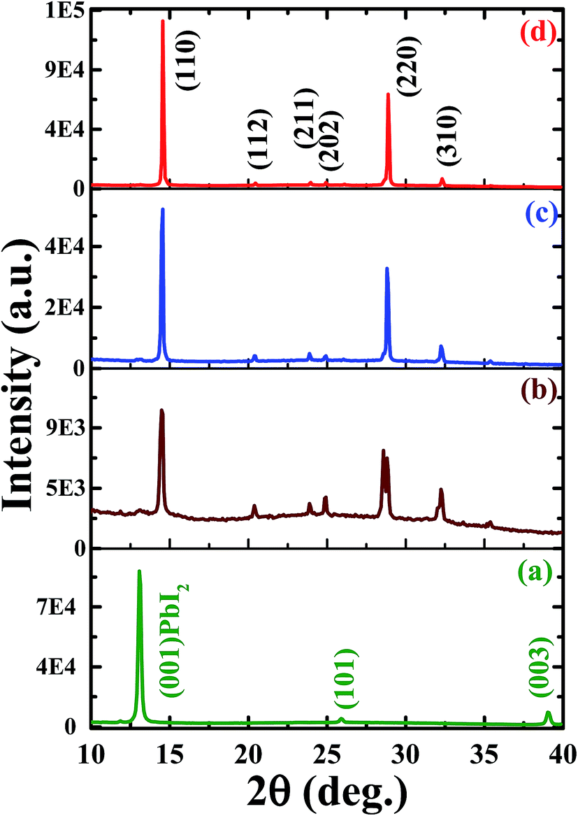 | ||
| Fig. 2 XRD patterns of (a) PbI2 film, (b) as-deposited perovskite film and perovskite films followed by (c) no MACl treatment and (d) MACl treatment. | ||
The top view of the perovskite films with and without MACl treatment, as depicted in Fig. 3, illustrates distinct surface morphology. The surface morphology of PbI2, as-grown perovskite, perovskite films with and without MACl treatment are shown in ESI† (Fig. S1). The grain sizes are broadly distributed ranging from 80–500 nm with an average size of ∼200 nm for perovskite films without MACl treatment whereas comparatively uniform grain sizes ranging from 150–500 nm with an average size of ∼300 nm are observed for the perovskite films with MACl treatment, which agrees with the crystallite size estimated from the XRD patterns and with the results of other reports.17,27,50
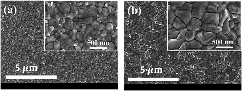 | ||
| Fig. 3 Top view SEM images of perovskite films ((a) without MACl treatment and (b) with MACl treatment [inset: magnified images]). | ||
We also studied the composition and distribution of constituent elements in fabricated films, as shown in ESI (Fig. S2 and S3†). No noticeable difference was found between the elemental compositions of the MACl-treated films and those of the untreated films. In particular, no additional chlorine is incorporated in MACl-treated films. This is in accordance with the well-matched XRD peaks of both types of films as depicted in Fig.2c and d. It indicates that the MACl treatment promotes crystal quality without any additional elemental incorporation in the perovskite film within the detection limit.
Furthermore, the perovskite films were characterized by XPS. We measured XPS spectra of the perovskite film surface and the bulk by etching the film by ∼80 nm, as shown in ESI (Fig. S4†). Although there is a dominant role played by MACl treatment on the perovskite film quality, the XPS characteristic feature of Cl2p core was absent within the detection limit in accordance with the report by Williams et al.49 The XPS characteristic features of I were found to be similar for both types of films. On the other hand, a distinct XPS characteristic feature pertaining to Pb was observed both on the surface and in the bulk of the perovskite films. As shown in Fig. S4a6 and b6,† the Pb peaks consist of two groups; the one with lower binding energy is assigned as Pb4f7/2 and that with the higher one as Pb4f5/2. The peaks at ∼137.6 and 142.7 eV are attributed to Pb in the perovskite structure.52,53 The additional small peaks around 135.7 and 141.9 eV marked with stars (*) may be due to the presence of unsaturated Pb.52
These results consolidate that the MACl treatment promotes better crystallinity coupled with compact, uniform, large grains and better film quality without making any noticeable change in stoichiometric and elemental distributions in the perovskite films.
The photophysical properties of perovskite films were investigated using absorption and PL spectra (Fig. 4), and we have collected UV-vis spectra of various films (Fig. S5†). The UV-vis spectra (Fig. S5c†) of the perovskite films with and without MACl treatment are similar except for a slight difference in the UV region. This trend is unaffected by the addition of HTL and ETL. The UV-vis spectra of PEDOT:PSS/perovskite and PEDOT:PSS/perovskite/PCBM layers (Fig. S5d and e†) are in accordance with Fig. S5c† when corrected for the absorption spectra of HTL and ETL (Fig. S5b†). Fig. 4a shows the room temperature PL spectra of respective perovskite films. The PL intensity of the perovskite film with MACl treatment was drastically enhanced (∼9 times) compared to that of films without MACl treatment. Furthermore, photoluminescence decay measurements (Fig. 4b) after fitting with a biexponential function revealed average carrier lifetimes of 235 and 136 ns in perovskite films with and without MACl treatment, respectively. These characteristic features of absorption, PL spectra, and PL decay are in good agreement with the results reported by Zhang et al.52 The enhancement in PL intensity and lifetime of perovskite films with MACl treatment is attributed to the improved crystallinity and larger grain sizes (Fig. 3). Non-radiative recombination centers provide decay channels of free carriers and these are likely to be energetic disorders and active defects. The better crystallinity will contribute to reduce them in the bulk while the larger grain sizes reduce the grain boundary. Similar improvement was reported in perovskite films processed with hypophosphorous acid.52
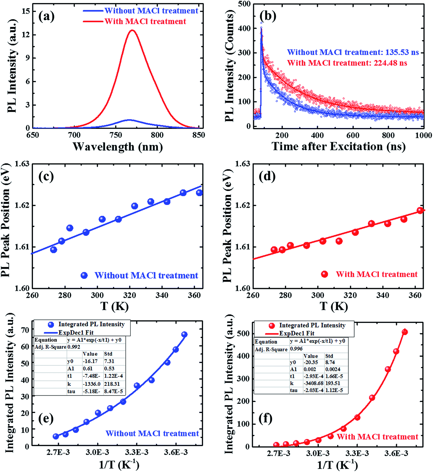 | ||
| Fig. 4 Photoluminescence (PL) spectra (a) and PL decay (b) of perovskite thin films with and without MACl treatment. The plots of temperature-dependent PL peak position (c and d) and integrated PL intensity (e and f) of respective films. The temperature-dependent PL spectra of perovskite films are depicted in Fig. S6 (ESI†). Here, the solid line in plots (c and d) represents a linear fitting whereas that in plots (e and f) represents a non-linear fitting. The inset table in plots (e and f) gives the fitting parameters. | ||
We also measured temperature-dependent PL spectra of perovskite films from 273 to 373 K as summarized in Fig. S6 (ESI†). With an increase in temperature, we observed a slight blue shift with faster broadening on the high energy side (Fig. 4c and d), in close agreement with the previous reports.54,55 We observed a slightly different temperature dependence in films with and without MACl treatment in terms of the quenching trend of PL intensity (Fig. S6a and b† and 4e and f). The temperature dependence of the PL peak position is 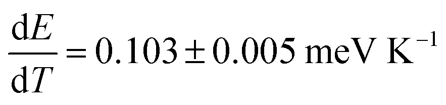 and 0.129 ± 0.015 meV K−1 for perovskite films with and without MACl treatment, respectively, which is analogous to the report by Wu et al.54 These results collectively support the fact that the perovskite films with MACl treatment have better quality as a consequence of reduction or mitigation of defect states and recombination activities, which will be further discussed in the later analysis.
Fig. 5 depicts cross-sectional SEM images of samples having the layered structure ITO/PEDOT:PSS/perovskite/PCBM/TBAI prior to silver electrode deposition to complete the device. The image of the MACl-untreated film (Fig. 5a) has mixed up features of grain sizes whereas that of the MACl-treated film (Fig. 5b) has comparatively well-grown large grains extending between the electrodes, which is beneficial for effective carrier transport and hence an efficient photovoltaic device.14,16,18
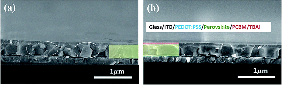 | ||
| Fig. 5 Cross-sectional SEM images of the ITO/PEDOT:PSS/perovskite/PCBM/TBAI structure having perovskite thin films (a) without MACl treatment and (b) with MACl treatment. | ||
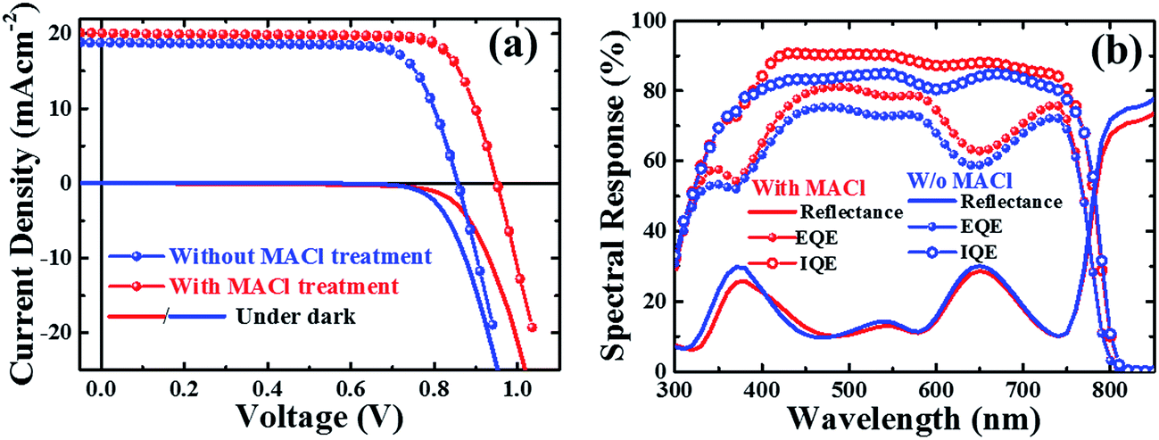
In order to see the effect of the film quality on the carrier recombination, we studied and compared the photovoltaic performance of the complete devices fabricated with and without MACl treatment. The current density–voltage (J–V) characteristics and the spectral response of champion PVSCs with and without MACl treatment are shown in Fig.6a. The PCEs of the two types of devices are 15.1% and 12.4%, respectively. We emphasize that all devices were fabricated under exactly the same conditions except for the MACl treatment. The device parameters are summarized in Table 1. The enhancement in VOC, FF and RSh for the MACl-treated device over the untreated device is much better compared to the enhancement in JSC and RS. The values of FF and RSh are comparable to the best reported.12,14,18,20,33 We also observed an enhancement in the diode ideality factor (A; 1.45 to 1.17) and reverse saturation current density (J0; 2.87 × 10⁻⁹ to 1.02 × 10⁻¹¹ mA cm−2) (Table 1), which are similar to the reports on CIGS and CZTS material-based thin film solar cell devices.56–58 We speculate that the improvement in the device parameters is due to reduction or mitigation of carrier recombination either at the interfaces or in the bulk of MACl-treated perovskite films as a consequence of improved crystallinity, morphology, and surface quality as discussed above. VOC and JSC could be improved by further optimization of bulk optoelectronic properties and tuning the charge transport material for better interface quality.17,19,35
 | ||
| Fig. 6 (a) Current density–voltage (J–V) characteristics and (b) spectral response of the perovskite devices with and without MACl treatment. | ||
| Device | J SC (mA cm−2) | V OC (V) | FF | η (%) | R S (Ω cm2) | R Sh (Ω cm2) | *A | *J0 (mA cm−2) |
|---|---|---|---|---|---|---|---|---|
| Without MACl | 18.78 | 0.86 | 0.77 | 12.41 | 4.31 | 3.58 × 10³ | 1.45 | 2.87 × 10⁻⁹ |
| With MACl | 20.06 | 0.95 | 0.79 | 15.09 | 4.52 | 1.70 × 10⁴ | 1.17 | 1.02 × 10⁻¹¹ |
The spectral responses of respective devices are presented in Fig. 6b. The device with MACl treatment revealed an enhanced EQE over a wide wavelength regime (∼330–750 nm). The values of JSC calculated by integrating the EQE are 18.92 and 17.89 mA cm−2 for devices with and without MACl treatment, respectively, which are found to be close to the values obtained from the respective J–V characteristics listed in Table 1. The EQE of PVSCs in the longer wavelength regime, λ > 500 nm, is strongly dependent on the quality of the perovskite material and interface whereas that of the short wavelength regime is strongly influenced by the interface layer and interface quality of devices.18,59 The IQE [EQE/(1 − R)] spectra of devices reached ∼80% and ∼90% on average in 370–750 nm for the respective devices. The reflection of incidence light by the ITO substrate or interface layers of the device is one of the limiting factors for further enhancement of photocurrent.18 Incidentally, we did not apply any antireflection means in this study; hence, the additional improvement in EQE is obvious.
Furthermore, a comparative study of EQE spectra measured under different bias voltages (Fig. S7a and b, ESI†) was performed. In devices without MACl treatment, the EQE spectra under a negative bias are much distorted from those under 0 V bias. The distortion is better illustrated by taking the ratio, EQE(0 V)/EQE(±xV) (Fig. S7c and d, ESI†). This is a clear indication of a stronger trap-assisted recombination59 in the device without MACl treatment than that in the MACl-treated device. We also calculated the band gap energy (Eg) of the perovskite layer by differentiating the EQE with respect to wavelength vs. energy 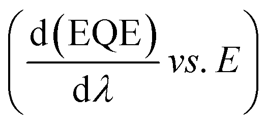 (Fig. S8†). The value (Eg = 1.57 ± 0.01 eV) is the same for both types of devices and is close to the value shown by PL spectra. These results support the fact that there are apparent influences on perovskite film quality by MACl treatment but no stoichiometric change, which is consistent with the results of XPS and XRD discussed above.
To elucidate the recombination of photogenerated carriers during device operation, we obtained the J–V curves of both types of devices as a function of light intensity as depicted in Fig. S9 (ESI†). The light intensity dependence of VOC and JSC can provide information about the recombination mechanism under open circuit conditions, where the photogenerated charge carriers recombine within the cell.60 We analyzed the light intensity-dependent VOC given by the relationship,60
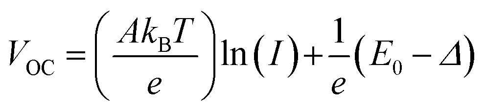 | (1) |
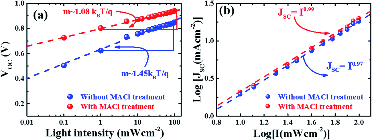 | ||
| Fig. 7 Plots of light intensity-dependent VOC (a) and JSC (b) of devices with and without MACl treatment. Here the dashed lines represent a linear fit to respective device parameters. | ||
For further confirmation, the electrical properties of devices were extracted by fitting J–V curves according to the diode model as described in reports.57,63,64 The plots for estimation of RS, RSh, J0, and A are shown in Fig. S10† and the deduced data are summarized in Table S1 in ESI.† Good agreement was found between the diode ideality factors calculated by using different approaches and measurements. Other electrical parameters of devices, RS, RSh, and GSh, also fall within the acceptable range. It is to be noted that the diode ideality factor is associated with the recombination mechanism. The value of A approaching 1 indicates that recombination dominates in the quasi neutral region (QNR) whereas if A approaches 2, the Shockley–Read–Hall (SRH) recombination mechanism in the space charge region (SCR) is important.57,58,65 In our case, the decrease in A from ∼1.5 for the device without MACl treatment to ∼1.15 for the device with MACl treatment indicates much reduced trap-assisted recombination losses in the latter, which is in good agreement with the results from the analysis of the light intensity dependence of VOC. It should be noted also that the reverse saturation current density (J0) decreases from 2.87 × 10⁻⁹ to 1.02 × 10⁻¹¹ mA cm−2 (Tables 1 and S1†) in going from a device without MACl treatment to that with the MACl treatment. J0 depends on defect activities especially in the absorber layer, which could have a strong influence on VOC and FF.57,64 Therefore, the decrease in J0 and the improvement in VOC and FF all point to the mitigation of the defect activities in MACl-treated devices.
To gain a more in-depth understanding on the carrier profile, defect level and defect distribution, the devices were investigated by using capacitance spectroscopy (Fig.8). We carried out capacitance–voltage (C–V) measurements and extracted the Mott–Schottky plot (Fig. 8a) and the carrier profile (Fig. 8b) was estimated by the relation,65
 | (2) |
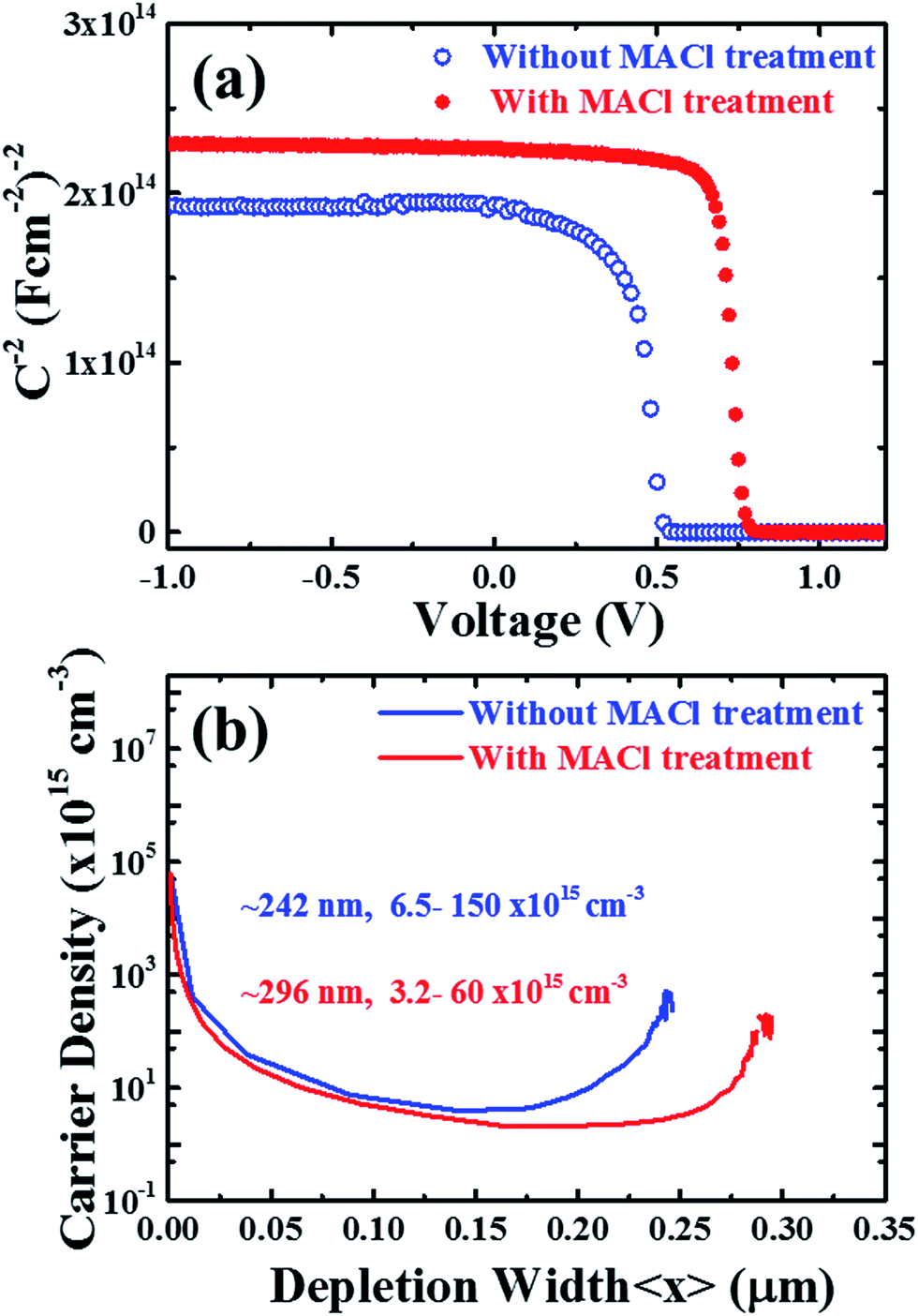 | ||
| Fig. 8 Mott–Schottky plot derived from the capacitance–bias voltage (C–V) response of the respective devices (a) and carrier density profiles (b) extracted from the C–V profile. The carrier density profile range given in the plot denotes the minimum carrier density and carrier density close to the SCR width. | ||
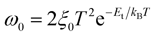
We further investigated the devices by using admittance spectroscopy (AS) to probe the defect energy level and defect density profile, which have been broadly employed in photovoltaic research for defect characterization (Fig. 9).65,68–71 The defect states in the absorber layer are estimated by employing the Arrhenius plot of characteristic transition frequencies ω0 expressed by the relation,
 | (3) |
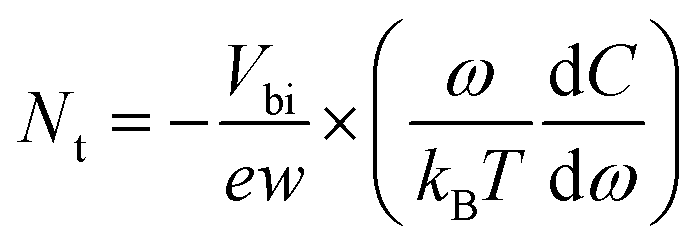 | (4) |
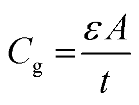 , where ε is the dielectric constant, A is the area and t is the thickness of the absorber layer as depicted in Fig. S11,† which was found to be ∼22 and 25 for devices with and without MACl treatment, respectively, showing good agreement with the report.64,72 The Arrhenius plots of characteristic frequencies (ω0), extracted from the differentiation of capacitance spectra (Fig. S12†) are depicted in Fig. 9c and the defect distribution in the corresponding defect levels are shown in Fig. 9d. It should be noted that both devices revealed two defect states. The device without MACl treatment showed two deep trap levels at E′t1 ∼ 0.467 eV and E′t2 ∼ 0.324 eV with emission factors (υ0), 5.68 × 10¹¹ and 5.76 × 10⁸ s−1, respectively which are close to the report by Shao et al.70 The device with MACl treatment demonstrated shallower trap levels at Et1 ∼ 0.346 eV and Et2 ∼ 0.241 eV with emission factors (υ′0), 1.258 × 10¹⁰ and 1.35 × 10⁸ s−1, respectively, which are in the range reported by Heo et al.73 The integrated defect densities (Fig. 9d) corresponding to the defect levels were found to be in the range of ∼1017 cm−3, which is comparable to the reports by other groups.68,70,73 In this analysis, the defect densities were found to be insensitive to the MACl treatment, but rather it eliminates deep defects. Deep defects are much more effective in the SRH recombination and hence the trap distribution difference in the MACl-treated and untreated devices corroborates well the difference in the respective optoelectronic performance and efficiency.
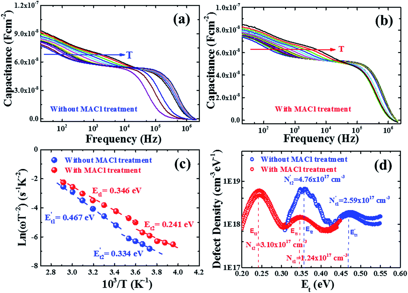 | ||
| Fig. 9 Capacitance frequency (C–f) response of the devices (without and with MACl treatment) (a and b) in the temperature range 243 K–353 K. The Arrhenius plot (c) and defect distribution profile (d) of the respective devices. | ||
Of course, the identification of the defect type is quite complicated. One can speculate that the defect levels estimated in our analysis could be related to either iodine lead antisites (IPb) or iodine interstitials (Ii), as reported by the density functional theory (DFT).69,74,75 It is thus quite interesting and challenging to correlate the effect of various fabrication processes with the resulting defect distributions. Only through this endeavor, can one reach a definitive conclusion.
In order to gain better insight into the relationship between the efficiency improvement and observed optoelectronic behavior of devices, we performed device simulation by using the program SCAPS (ver. 3.3.01)76 and a solar cell capacitance simulator, which is a numerical tool to simulate the impact of properties of layers and interfaces on the device performance.77,78 Since the perovskite device of the planar structure is close to that of typical thin film PV cells, device simulation was carried out by adopting the device layers shown in Fig. S13,† thereby resembling the real device with the layer properties, as summarized in Table S2.†79,80 The simulation was carried out to account for the material and interface quality by considering the bulk and interface defect densities and other layer properties by mimicking experimental results as close as possible. The simulated J–V characteristics demonstrate a good agreement with the general feature of experimental results of the respective type of devices, as depicted in Fig. S14.† Although there is a slight discrepancy in FF, the simulated device parameters are close enough to experimental results (Table S3†). The simulated energy band diagrams of the respective type of devices are shown in Fig. S15† and are quite similar. In contrast, the simulation results (Fig. S16†) show a higher generation current density and lower recombination current density in the MACl-treated device, which supports alleviation of defect activities as revealed in the experimental results. The device simulation taking into account the interface and bulk defect profile relating to the layer quality as depicted in Fig. S17† illustrates their impact on J–V characteristics, which conforms to the experimental results.
The fabricated devices were statistically compared by plotting the histograms of device parameters (η, JSC, VOC, and FF), as shown in Fig.10. The histograms were deduced from 60 devices prepared with or without MACl treatment in 5 batches. The results are summarized in Table 2. The standard deviations of all device parameters for devices with MACl treatment are smaller than those without MACl treatment. 80% of devices fabricated with MACl treatment yield a PCE >14% indicating outstanding reproducibility. It is believed that the efficiency can be further improved to a competitive high value26,34 by addressing some critical issues related to the bulk film quality and introducing more efficient charge transport layers for better optoelectronic properties and carrier dynamics.
 | ||
| Fig. 10 Histogram of device parameters: (a) PEC (η), (b) JSC, (c) VOC, and (d) FF of 60 devices (devices with and without MACl treatment). | ||
| Statistics of devices | Without MACl | With MACl | ||||||
|---|---|---|---|---|---|---|---|---|
| J SC (mA cm−2) | V OC (V) | FF | η (%) | J SC (mA cm−2) | V OC (V) | FF | η (%) | |
| Avg | 17.59 | 0.85 | 0.75 | 11.27 | 19.76 | 0.93 | 0.77 | 14.33 |
| Max | 18.96 | 0.91 | 0.79 | 12.41 | 20.53 | 0.96 | 0.80 | 15.09 |
| Min | 15.04 | 0.78 | 0.70 | 10.29 | 17.52 | 0.88 | 0.72 | 13.34 |
| STD | 1.07 | 0.03 | 0.02 | 0.66 | 0.51 | 0.02 | 0.01 | 0.50 |
We also monitored the aging effect on the performance of encapsulated devices stored under ambient conditions. J–V characteristics of devices were measured periodically as depicted in Fig.11. The stability data of more devices are shown in Fig. S18 (ESI†). It is observed that there is almost no loss in JSC and FF of both types of devices over the period whereas the device efficiencies decreased slowly after 30 days due to the decrease in VOC. The loss in VOC might be caused either by an increase in trap centers and defect activities or worsening of the interface. The loss in efficiency and VOC is comparatively slow for MACl-treated devices. The MACl-treated devices retained ∼90% of their initial efficiency after 90 days, while the devices without the MACl treatment preserved ∼80% of their initial efficiency over the same period. These values are comparable to the previous reports.27,50 It is to be noted that hysteresis in the JV curve was not observed over the aging time as depicted in Fig. S19.† This observation is similar to our previous report.50 Even though the origin of the hysteresis effect is a matter of strong debate,23 the hysteresis issue has been well-addressed by adjusting the charge transport layer.4,70 Moreover, the causes of degradation of our device are not related to the hysteresis either. However, mitigation of defects in the bulk and interface, better transport layers, control of ion migration and poor humidity tolerance are still big issues to address for the commercial viability of PVSCs.
 | ||
| Fig. 11 Stability data (solar cell parameters JSC, VOC, FF, and η) of encapsulated devices stored under ambient conditions for 3 months. | ||
3. Conclusion
We report the improvement in device efficiency, stability, and reproducibility of low temperature solution-processed planar perovskite devices with perovskite thin films annealed in a MACl vapor atmosphere. This approach demonstrated better grain morphology and enhanced PL spectra in perovskite thin films. The analysis of device characteristics and capacitance spectra revealed an enhancement in optoelectronic properties with reduction of defect activities and passivation of defect levels, which, we infer, reduce recombination loss. These improvements lead to better device efficiency with reproducibility coupled with promising stability by retaining more than 90% of their initial performance over 60 days. Further progress in device efficiency requires better film and interface quality and defect passivation.4. Experimental section
Materials and preparation
All chemicals were purchased from commercial suppliers as mentioned and unless otherwise specified, they were used as received. Methyl ammonium iodide (MAI) and methyl ammonium chloride (MACl) were of battery grade and were obtained from Wako chemical company. For the fabrication of perovskite films, precursor solutions were prepared by dissolving the PbI2–DMSO complex (prepared according to literature17) in anhydrous DMF (500 mg ml−1), and MAI and MACl in ethanol (50 mg ml−1; 19![[thin space (1/6-em)]](https://www.rsc.org/images/entities/char_2009.gif) :1 ratio). [6,6]-Phenyl C61 butyric acid methyl ester (PC61BM) [Sigma Aldrich, 99% purity] solution (2 wt%) dissolved in anhydrous chlorobenzene (CB) was used for coating of the electron transport layer (ETL). Tetrabutylammonium iodide (TBAI) (Sigma Aldrich, 99% purity) precursor solution was prepared in ethanol for doping of the PCBM surface facing the cathode metal.81 All the solutions were filtered by using 0.45 μm syringe filters to avoid the risk of unwanted particles in the precursor solution.
:1 ratio). [6,6]-Phenyl C61 butyric acid methyl ester (PC61BM) [Sigma Aldrich, 99% purity] solution (2 wt%) dissolved in anhydrous chlorobenzene (CB) was used for coating of the electron transport layer (ETL). Tetrabutylammonium iodide (TBAI) (Sigma Aldrich, 99% purity) precursor solution was prepared in ethanol for doping of the PCBM surface facing the cathode metal.81 All the solutions were filtered by using 0.45 μm syringe filters to avoid the risk of unwanted particles in the precursor solution.
Device fabrication
Solar cell devices were fabricated on pre-cleaned patterned indium tin oxide (ITO) coated glass substrates (15 Ω per square). The ITO substrates were pre-cleaned in an ultrasonic bath with detergent, pure water, and 2-propanol, followed by an ultraviolet-ozone treatment for 5 min to remove the organic residuals. A thin HTM layer (30 nm) of poly(3,4-ethylenedioxythiophene):poly(styrene sulfonate) (PEDOT:PSS, Clevios, Al4083) was deposited by spin coating at 3000 rpm and subsequently dried at 130 °C for 10 min on a hot plate in air ambient. Then, the substrates were transferred to a nitrogen-filled glove box (<1.0 ppm O2 and H2O) and the rest of the steps were carried out inside the glove box. PbI2 precursor solution was spin coated at 3000 rpm for 90 s and a mixed precursor solution of MAI and MACl was subsequently spun on to the PbI2 layer at 4000 rpm for 30 s. Then to promote the crystallization, those as grown CH3NH3PbI3−xClx perovskite films were simply placed inside a Petri dish with or without MACl powders on a hot plate at 100 °C for MACl treatment (Fig. S20†). For the ETM layer, PC61BM was spin-coated on top of the perovskite films at 700 rpm for 30 s coupled at 5000 rpm for 10 s, followed by deposition of a thin TBAI layer that was spun at 3000 rpm for 25 s. To complete the device structure, the samples were then transferred into the evaporation chamber connected to the glove box for metal contact deposition. Finally, 100 nm of Ag was thermally evaporated at a pressure <10−4 Pa. Devices with an area of 0.26 cm2 were sealed by using UV-curable resins (UVRESIN XNR5516Z, NagaseChemteX, Japan) before performing the subsequent measurements under ambient conditions.Device characterization
The X-ray diffraction (XRD) patterns of fabricated perovskite films were collected using a Bruker D8 advanced X-ray diffractometer (CuKα radiation, λ = 1.54050 Å). The morphology of films and cross-sectional images were obtained by using a high resolution scanning electron microscope (SEM) at a 5 kV accelerating voltage (Hitachi, S-4800). The absorption spectra and photoluminescence (PL) spectra of various films were recorded using a UV-vis-NIR spectrometer (7200, V-Jasco) and a Spectrofluorometer (FP8500, Jasco). The carrier lifetimes were measured with a fluorescence lifetime spectrometer (Quantaurus-τ from Hamamatsu-Photonics K.K.). The current density–voltage (J–V) characteristics and spectral response (incident monochromatic photon to current conversion efficiency (IPCE) spectra, external quantum efficiency (EQE), and reflectance spectra) were characterized with a spectrometer (SM-250IQE, Bunkokeiki, Japan) by using an aperture mask with 0.185 cm2 openings. The capacitance–frequency response (C–f) was measured with an LCR meter (E4980A, Agilent), which probes from 20 Hz to 2 MHz at an ac voltage amplitude of 10 mV under dark conditions in the temperature range of 253–343 K, whereas capacitance–voltage (C–V) measurements were carried out at 1 kHz. For temperature dependent C–f scans, a temperature-controlled chamber (SU-221) was used by having a control system with an error of ±0.1 K (°C).Acknowledgements
The authors acknowledge the support from the MEXT Program for Development of Environment Technology using Nanotechnology.References
- A. Kojima, K. Teshima, Y. Shirai and T. Miyasaka, J. Am. Chem. Soc., 2009, 131, 6050–6051 CrossRef CAS PubMed.
- M. A. Green, K. Emery, Y. Hishikawa, W. Warta, E. D. Dunlop, D. H. Levi and A. W. Y. Ho-Baillie, Progress in Photovoltaics: Research and Applications, 2017, 25, 3–13 CrossRef.
- K. Leo, Nat. Nanotechnol., 2015, 10, 574–575 CrossRef CAS PubMed.
- M. A. Green, A. Ho-Baillie and H. J. Snaith, Nat. Photonics, 2014, 8, 506–514 CrossRef CAS.
- J. H. Heo, S. H. Im, J. H. Noh, T. N. Mandal, C. S. Lim, J. A. Chang, Y. H. Lee, H. J. Kim, A. Sarkar, M. K. Nazeeruddin, M. Gratzel and S. I. Seok, Nat. Photonics, 2013, 7, 486–491 CrossRef CAS.
- A. Miyata, A. Mitioglu, P. Plochocka, O. Portugall, J. T.-W. Wang, S. D. Stranks, H. J. Snaith and R. J. Nicholas, Nat. Phys., 2015, 11, 582–587 CrossRef CAS.
- S. D. Stranks, G. E. Eperon, G. Grancini, C. Menelaou, M. J. P. Alcocer, T. Leijtens, L. M. Herz, A. Petrozza and H. J. Snaith, Science, 2013, 342, 341–344 CrossRef CAS PubMed.
- M. I. Saidaminov, A. L. Abdelhady, B. Murali, E. Alarousu, V. M. Burlakov, W. Peng, I. Dursun, L. Wang, Y. He, G. Maculan, A. Goriely, T. Wu, O. F. Mohammed and O. M. Bakr, Nat. Commun., 2015, 6, 7586 CrossRef PubMed.
- W. S. Yang, J. H. Noh, N. J. Jeon, Y. C. Kim, S. Ryu, J. Seo and S. I. Seok, Science, 2015, 348, 1234–1237 CrossRef CAS PubMed.
- Y. Ogomi, A. Morita, S. Tsukamoto, T. Saitho, N. Fujikawa, Q. Shen, T. Toyoda, K. Yoshino, S. S. Pandey, T. L. Ma and S. Hayase, J. Phys. Chem. Lett., 2014, 5, 1004–1011 CrossRef CAS PubMed.
- J. H. Noh, S. H. Im, J. H. Heo, T. N. Mandal and S. I. Seok, Nano Lett., 2013, 13, 1764–1769 CrossRef CAS PubMed.
- J. Burschka, N. Pellet, S. J. Moon, R. Humphry-Baker, P. Gao, M. K. Nazeeruddin and M. Gratzel, Nature, 2013, 499, 316–319 CrossRef CAS PubMed.
- Y. Deng, Q. Dong, C. Bi, Y. Yuan and J. Huang, Adv. Energy Mater., 2016, 6, 1600372 CrossRef.
- M. Z. Liu, M. B. Johnston and H. J. Snaith, Nature, 2013, 501, 395–398 CrossRef CAS PubMed.
- J. You, Z. Hong, Y. Yang, Q. Chen, M. Cai, T.-B. Song, C.-C. Chen, S. Lu, Y. Liu, H. Zhou and Y. Yang, ACS Nano, 2014, 8, 1674–1680 CrossRef CAS PubMed.
- Z. Xiao, C. Bi, Y. Shao, Q. Dong, Q. Wang, Y. Yuan, C. Wang, Y. Gao and J. Huang, Energy Environ. Sci., 2014, 7, 2619–2623 CAS.
- N. J. Jeon, J. H. Noh, Y. C. Kim, W. S. Yang, S. Ryu and S. Il Seol, Nat. Mater., 2014, 13, 897–903 CrossRef CAS PubMed.
- Z. Xiao, Q. Dong, C. Bi, Y. Shao, Y. Yuan and J. Huang, Adv. Mater., 2014, 26, 6503–6509 CrossRef CAS PubMed.
- Z. M. Zhou, Z. W. Wang, Y. Y. Zhou, S. P. Pang, D. Wang, H. X. Xu, Z. H. Liu, N. P. Padture and G. L. Cui, Angew. Chem., Int. Ed., 2015, 54, 9705–9709 CrossRef CAS PubMed.
- F. Fu, T. Feurer, T. Jäger, E. Avancini, B. Bissig, S. Yoon, S. Buecheler and A. N. Tiwari, Nat. Commun., 2015, 6, 8932 CrossRef CAS PubMed.
- C.-C. Chueh, C.-Z. Li and A. K. Y. Jen, Energy Environ. Sci., 2015, 8, 1160–1189 CAS.
- J. You, L. Meng, T.-B. Song, T.-F. Guo, Y. Yang, W.-H. Chang, Z. Hong, H. Chen, H. Zhou, Q. Chen, Y. Liu, N. De Marco and Y. Yang, Nat. Nanotechnol., 2016, 11, 75–81 CrossRef CAS PubMed.
- H. J. Snaith, A. Abate, J. M. Ball, G. E. Eperon, T. Leijtens, N. K. Noel, S. D. Stranks, J. T. W. Wang, K. Wojciechowski and W. Zhang, J. Phys. Chem. Lett., 2014, 5, 1511–1515 CrossRef CAS PubMed.
- K. Miyano, M. Yanagida, N. Tripathi and Y. Shirai, J. Phys. Chem. Lett., 2016, 2240–2245, DOI:10.1021/acs.jpclett.6b00579.
- D. Wang, M. Wright, N. K. Elumalai and A. Uddin, Sol. Energy Mater. Sol. Cells, 2016, 147, 255–275 CrossRef CAS.
- J. H. Heo, H. J. Han, D. Kim, T. K. Ahn and S. H. Im, Energy Environ. Sci., 2015, 8, 1602–1608 CAS.
- N. Tripathi, M. Yanagida, Y. Shirai, T. Masuda, L. Han and K. Miyano, J. Mater. Chem. A, 2015, 3, 12081–12088 CAS.
- Q. Chen, N. De Marco, Y. Yang, T.-B. Song, C.-C. Chen, H. Zhao, Z. Hong, H. Zhou and Y. Yang, Nano Today, 2015, 10, 355–396 CrossRef CAS.
- G. E. Eperon, V. M. Burlakov, P. Docampo, A. Goriely and H. J. Snaith, Adv. Funct. Mater., 2014, 24, 151–157 CrossRef CAS.
- A. Dualeh, N. Tétreault, T. Moehl, P. Gao, M. K. Nazeeruddin and M. Grätzel, Adv. Funct. Mater., 2014, 24, 3250–3258 CrossRef CAS.
- Q. Chen, H. P. Zhou, Z. R. Hong, S. Luo, H. S. Duan, H. H. Wang, Y. S. Liu, G. Li and Y. Yang, J. Am. Chem. Soc., 2014, 136, 622–625 CrossRef CAS PubMed.
- P. Docampo, F. C. Hanusch, S. D. Stranks, M. Döblinger, J. M. Feckl, M. Ehrensperger, N. K. Minar, M. B. Johnston, H. J. Snaith and T. Bein, Adv. Energy Mater., 2014, 4, 1400355 CrossRef.
- C.-H. Chiang and C.-G. Wu, Nat. Photonics, 2016, 10, 196–200 CrossRef CAS.
- M. Saliba, T. Matsui, J.-Y. Seo, K. Domanski, J.-P. Correa-Baena, M. K. Nazeeruddin, S. M. Zakeeruddin, W. Tress, A. Abate, A. Hagfeldt and M. Grätzel, Energy Environ. Sci., 2016, 9, 1989–1997 CAS.
- M. Hu, C. Bi, Y. Yuan, Y. Bai and J. Huang, Adv. Sci., 2016, 3, 1500301 CrossRef PubMed.
- M. D. Xiao, F. Z. Huang, W. C. Huang, Y. Dkhissi, Y. Zhu, J. Etheridge, A. Gray-Weale, U. Bach, Y. B. Cheng and L. Spiccia, Angew. Chem., Int. Ed., 2014, 53, 9898–9903 CrossRef CAS PubMed.
- X. Song, W. W. Wang, P. Sun, W. L. Ma and Z. K. Chen, Appl. Phys. Lett., 2015, 106, 033901 CrossRef.
- P.-W. Liang, C.-Y. Liao, C.-C. Chueh, F. Zuo, S. T. Williams, X.-K. Xin, J. Lin and A. K. Y. Jen, Adv. Mater., 2014, 26, 3748–3754 CrossRef CAS PubMed.
- H. B. Kim, H. Choi, J. Jeong, S. Kim, B. Walker, S. Song and J. Y. Kim, Nanoscale, 2014, 6, 6679–6683 RSC.
- W. Zhang, M. Saliba, D. T. Moore, S. K. Pathak, M. T. Horantner, T. Stergiopoulos, S. D. Stranks, G. E. Eperon, J. A. Alexander-Webber, A. Abate, A. Sadhanala, S. H. Yao, Y. L. Chen, R. H. Friend, L. A. Estroff, U. Wiesner and H. J. Snaith, Nat. Commun., 2015, 6, 6142 CrossRef CAS PubMed.
- Y. Zhou, M. Yang, W. Wu, A. L. Vasiliev, K. Zhu and N. P. Padture, J. Mater. Chem. A, 2015, 3, 8178–8184 CAS.
- H. Yu, X. Liu, Y. Xia, Q. Dong, K. Zhang, Z. Wang, Y. Zhou, B. Song and Y. Li, J. Mater. Chem. A, 2016, 4, 321–326 CAS.
- Y. Zhou, M. Yang, O. S. Game, W. Wu, J. Kwun, M. A. Strauss, Y. Yan, J. Huang, K. Zhu and N. P. Padture, ACS Appl. Mater. Interfaces, 2016, 8, 2232–2237 CAS.
- E. L. Unger, A. R. Bowring, C. J. Tassone, V. L. Pool, A. Gold-Parker, R. Cheacharoen, K. H. Stone, E. T. Hoke, M. F. Toney and M. D. McGehee, Chem. Mater., 2014, 26, 7158–7165 CrossRef CAS.
- A. Dualeh, P. Gao, S. I. Seok, M. K. Nazeeruddin and M. Grätzel, Chem. Mater., 2014, 26, 6160–6164 CrossRef CAS.
- M. Yang, Y. Zhou, Y. Zeng, C.-S. Jiang, N. P. Padture and K. Zhu, Adv. Mater., 2015, 27, 6363–6370 CrossRef CAS PubMed.
- E. Edri, S. Kirmayer, S. Mukhopadhyay, K. Gartsman, G. Hodes and D. Cahen, Nat. Commun., 2014, 5, 3461 Search PubMed.
- H. Yu, F. Wang, F. Xie, W. Li, J. Chen and N. Zhao, Adv. Funct. Mater., 2014, 24, 7102–7108 CAS.
- S. T. Williams, F. Zuo, C. C. Chueh, C. Y. Liao, P. W. Liang and A. K. Y. Jen, ACS Nano, 2014, 8, 10640–10654 CrossRef CAS PubMed.
- N. Tripathi, Y. Shirai, M. Yanagida, A. Karen and K. Miyano, ACS Appl. Mater. Interfaces, 2016, 8, 4644–4650 CAS.
- A. L. Patterson, Phys. Rev., 1939, 56, 978–982 CrossRef CAS.
- W. Zhang, S. Pathak, N. Sakai, T. Stergiopoulos, P. K. Nayak, N. K. Noel, A. A. Haghighirad, V. M. Burlakov, D. W. deQuilettes, A. Sadhanala, W. Li, L. Wang, D. S. Ginger, R. H. Friend and H. J. Snaith, Nat. Commun., 2015, 6, 10030 CrossRef CAS PubMed.
- G. Sadoughi, D. E. Starr, E. Handick, S. D. Stranks, M. Gorgoi, R. G. Wilks, M. Bär and H. J. Snaith, ACS Appl. Mater. Interfaces, 2015, 7, 13440–13444 CAS.
- K. Wu, A. Bera, C. Ma, Y. Du, Y. Yang, L. Li and T. Wu, PCCP Phys. Chem. Chem. Phys., 2014, 16, 22476–22481 RSC.
- B. J. Foley, D. L. Marlowe, K. Sun, W. A. Saidi, L. Scudiero, M. C. Gupta and J. J. Choi, Appl. Phys. Lett., 2015, 106, 243904 CrossRef.
- W. Wang, M. T. Winkler, O. Gunawan, T. Gokmen, T. K. Todorov, Y. Zhu and D. B. Mitzi, Adv. Energy Mater., 2014, 4, 1301465 CrossRef.
- D. B. Khadka, S. Kim and J. Kim, J. Phys. Chem. C, 2016, 120, 4251–4258 CAS.
- T. Gershon, T. Gokmen, O. Gunawan, R. Haight, S. Guha and B. Shin, MRS Commun., 2014, 4, 159–170 CrossRef CAS.
- Q. Lin, A. Armin, R. C. R. Nagiri, P. L. Burn and P. Meredith, Nat. Photonics, 2015, 9, 106–112 CrossRef CAS.
- S. R. Cowan, A. Roy and A. J. Heeger, Phys. Rev. B: Condens. Matter Mater. Phys., 2010, 82, 245207 CrossRef.
- V. V. Brus, C. M. Proctor, N. A. Ran and T.-Q. Nguyen, Adv. Energy Mater., 2016, 6, 1502250 CrossRef.
- M. Jahandar, J. H. Heo, C. E. Song, K.-J. Kong, W. S. Shin, J.-C. Lee, S. H. Im and S.-J. Moon, Nano Energy, 2016, 27, 330–339 CrossRef CAS.
- S. S. Hegedus and W. N. Shafarman, Progress in Photovoltaics: Research and Applications, 2004, 12, 155–176 CrossRef CAS.
- K. Miyano, M. Yanagida, N. Tripathi and Y. Shirai, Appl. Phys. Lett., 2015, 106, 093903 CrossRef.
- J. Heath and P. Zabierowski, in Advanced Characterization Techniques for Thin Film Solar Cells, Wiley-VCH Verlag GmbH & Co. KGaA, 2011, pp. 81–105, DOI:10.1002/9783527636280.ch4.
- H. Tsai, W. Nie, J.-C. Blancon, C. C. Stoumpos, R. Asadpour, B. Harutyunyan, A. J. Neukirch, R. Verduzco, J. J. Crochet, S. Tretiak, L. Pedesseau, J. Even, M. A. Alam, G. Gupta, J. Lou, P. M. Ajayan, M. J. Bedzyk, M. G. Kanatzidis and A. D. Mohite, Nature, 2016, 536, 312–316 CrossRef CAS PubMed.
- K. Miyano, N. Tripathi, M. Yanagida and Y. Shirai, Acc. Chem. Res., 2016, 49, 303–310 CrossRef CAS PubMed.
- H.-S. Duan, H. Zhou, Q. Chen, P. Sun, S. Luo, T.-B. Song, B. Bob and Y. Yang, Phys. Chem. Chem. Phys., 2015, 17, 112–116 RSC.
- W.-J. Yin, J.-H. Yang, J. Kang, Y. Yan and S.-H. Wei, J. Mater. Chem. A, 2015, 3, 8926–8942 CAS.
- Y. Shao, Z. Xiao, C. Bi, Y. Yuan and J. Huang, Nat. Commun., 2014, 5, 5784 CrossRef CAS PubMed.
- D. B. Khadka, S. Kim and J. Kim, J. Phys. Chem. C, 2015, 119, 12226–12235 CAS.
- I. Zarazua, J. Bisquert and G. Garcia-Belmonte, J. Phys. Chem. Lett., 2016, 7, 525–528 CrossRef CAS PubMed.
- J. H. Heo, D. H. Song, H. J. Han, S. Y. Kim, J. H. Kim, D. Kim, H. W. Shin, T. K. Ahn, C. Wolf, T.-W. Lee and S. H. Im, Adv. Mater., 2015, 27, 3424–3430 CrossRef CAS PubMed.
- M. H. Du, J. Mater. Chem. A, 2014, 2, 9091–9098 CAS.
- J. M. Azpiroz, E. Mosconi, J. Bisquert and F. De Angelis, Energy Environ. Sci., 2015, 8, 2118–2127 CAS.
- M. Burgelman, P. Nollet and S. Degrave, Thin Solid Films, 2000, 361–362, 527–532 CrossRef CAS.
- J. Pettersson, M. Edoff and C. Platzer-Björkman, J. Appl. Phys., 2012, 111, 014509 CrossRef.
- A. Chirilă, S. Buecheler, F. Pianezzi, P. Bloesch, C. Gretener, A. R. Uhl, C. Fella, L. Kranz, J. Perrenoud, S. Seyrling, R. Verma, S. Nishiwaki, Y. E. Romanyuk, G. Bilger and A. N. Tiwari, Nat. Mater., 2011, 10, 857–861 CrossRef PubMed.
- F. Liu, J. Zhu, J. F. Wei, Y. Li, M. Lv, S. F. Yang, B. Zhang, J. X. Yao and S. Y. Dai, Appl. Phys. Lett., 2014, 104, 253508 CrossRef.
- T. Minemoto and M. Murata, J. Appl. Phys., 2014, 116, 054505 CrossRef.
- C. Z. Li, C. C. Chueh, F. Z. Ding, H. L. Yip, P. W. Liang, X. S. Li and A. K. Y. Jen, Adv. Mater., 2013, 25, 4425–4430 CrossRef CAS PubMed.
Footnote |
| † Electronic supplementary information (ESI) available. See DOI: 10.1039/c7se00033b |
| This journal is © The Royal Society of Chemistry 2017 |