
Atomic layer deposition for perovskite solar cells: research status, opportunities and challenges†
V.
Zardetto
a,
B. L.
Williams
a,
A.
Perrotta
a,
F.
Di Giacomo
b,
M. A.
Verheijen
ac,
R.
Andriessen
b,
W. M. M.
Kessels
ab and
M.
Creatore
*ab
aDepartment of Applied Physics, Eindhoven University of Technology, P.O. Box 513, 5600 MB Eindhoven, The Netherlands. E-mail: m.creatore@tue.nl; Tel: +31-402474223
bSolliance – Holst Centre, High Tech Campus 21, 5656 AE Eindhoven, The Netherlands
cPhilips Innovation Labs, High Tech Campus 11, 5656AE Eindhoven, The Netherlands
First published on 6th February 2017
Abstract
Atomic layer deposition is widely acknowledged as a powerful technique for the deposition of high quality layers for several applications including photovoltaics (PV). The capability of ALD to generate dense, conformal, virtually pinhole-free layers becomes attractive also for the emerging organo-metal halide perovskite solar cells (PSCs), which have garnered the interest of the PV community through their remarkable efficiency gains, now over 20%, in just a few years of research. Until now, the application of ALD layers in PSCs has almost exclusively been restricted to the stages of device fabrication prior to perovskite deposition. Researchers have mainly focused on fabricating efficient electron and hole transport layers (TiO2, SnO2, ZnO, NiO) and ultra-thin Al2O3 or TiO2 passivation layers for several device configurations. The first section of this contribution reviews the current state-of-the-art ALD for perovskite solar cells. Then, we explore other potential opportunities, such as the fabrication of doped metal oxide selective contacts and transparent electrodes, also for use in tandem solar cell architectures, as well as barrier layers for encapsulation. Finally, we present our own experimental investigation of the challenges involved in depositing directly on perovskite absorbers in view of replacing organic electron and hole transport layers with ALD metal oxides (MOs). Therefore, the effects of temperature, oxidizing agents and metal precursors on perovskite are studied. A number of insights are gained which can lead to the development of ad hoc ALD processes that are compatible with the underlying perovskite, in this case, methylammonium lead iodide, MAPbI3. The phase purity and surface chemistry of the perovskite were used as metrics to quantify the feasibility of depositing selected MOs which can be adopted as selective contacts and passivation layers.
1. Introduction
Atomic layer deposition (ALD) has been established as a versatile and robust deposition technique to generate high-quality thin-films of inorganic materials such as oxides, nitrides, sulphides, and metals.1–3 Since ALD operates via the sequential repetition of self-limiting surface reactions, (see Fig. 1) thin-film deposition can be controlled at the sub-nanometer scale, thereby enabling the fabrication of continuous, dense and virtually pinhole-free layers. This self-limiting nature of ALD reactions also results in excellent surface coverage and unrivalled conformality for thin film coatings on complex structures such as high aspect ratio substrates, porous materials, nanoparticles, and 3D architectures.1 Furthermore, the atomic scale control enables fine tuning of the optical, chemical and electronic properties of films, such as the film density, stoichiometry, and (intentional) doping level.3–5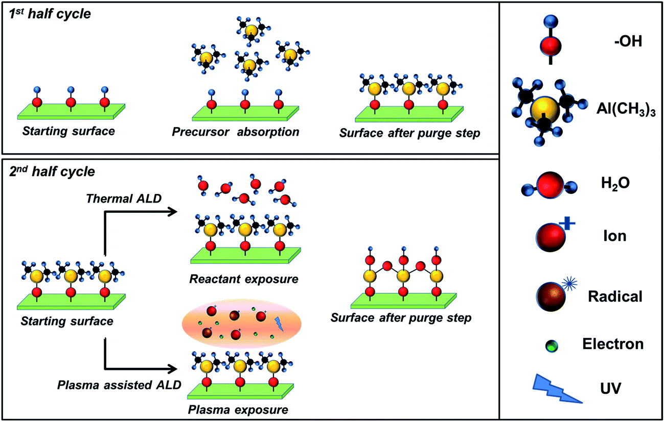 | ||
| Fig. 1 Schematic representation of one ALD cycle for a binary compound (e.g., Al2O3). Self-limiting reactions occur between the OH-terminated surface and the Al-precursor (tri-methyl-aluminum) (first half-cycle), and the co-reactant (second half-cycle). The co-reactant is H2O in the case of thermal ALD or O2 plasma in the case of a plasma assisted ALD process.3 The purge steps avoid parasitic CVD contribution during the ALD process leading to the desired accurate control of film thickness by repeating the ALD cycle. | ||
While the interest in ALD has been primarily driven by the requirement for down-scaling of features in the microelectronics industry,1,3,6 the benefits of this technique have been acknowledged for many other applications including electrochemical storage,7,8 catalysis,9–11 gas/vapor permeation barriers,12,13 bio-materials,14 and photovoltaics (PV). Extensive and complete overviews of the role of ALD layers in the performance of PV devices, including crystalline-Si, copper indium gallium diselenide (CIGS), organic (OPV) and dye-sensitized solar cells (DSSCs), have recently been published.15,16 However, in the last few years, a new class of solar cells based on perovskite organo-lead mixed halide absorbers (i.e., CH3NH3PbI3−x(Cl,Br)x, or briefly MAPbX3) has suddenly appeared in the PV landscape, with a significant impact on the PV research community. The main reasons for the widespread interest in perovskite solar cells (PSCs) include the remarkable increase in device performance (reaching slightly over 22% of power conversion efficiency on a small area in less than 4 years of research),17 the low temperature processes (below 150 °C), and the relatively simple solution and/or printing deposition methods. Therefore, the combination of high performance and low cost manufacturing processes would potentially provide a rapid energy payback time for future perovskite PV systems. Furthermore, large attention is focused on the opportunity for these devices to be efficient wide band-gap top cells in tandem configurations (combined with c-Si or CIGS bottom cells).18,19 Compared to other leading PV technologies, there are a number of exciting opportunities for PSCs to benefit from the use of ALD processing and a contribution about the advance of ALD for perovskite solar cells has very recently been published.20 Different from the last where the applications of ALD layers have been highlighted in few cases, the scope of our manuscript is to offer a complete review about all the several materials and ALD processes adopted thus far for perovskite PV devices, and at the same time to explore novel opportunities evaluating also the numerous technical challenges that are still to be addressed. First, in Section 2, we briefly describe the key material properties of perovskites and the variety of device configurations that have been developed. Then, in Section 3, examples of the successful introduction of ALD layers in perovskite cell architectures thus far are reviewed, including the development of layers for interfacial engineering, tandem-cell integration, and device encapsulation. Feasible and potential opportunities will also be discussed to fully exploit ALD as a technique enabling an increase in perovskite efficiency, large area processing and device stability. Finally, in Section 4, we point out the technical challenges faced by researchers in integrating ALD processing on top of perovskite structures. We conclude by presenting new results from our group monitoring the effect of processing ALD films (temperatures, co-reactants and types of metal oxides) directly over the perovskite layers by means of X-ray diffraction (XRD) and X-ray photoelectron spectroscopy (XPS), providing useful information for the future development of ad hoc ALD processes for the perovskite technology.
2. Perovskite solar cells: configurations and technical challenges
Perovskite solar cells have historically emerged as a natural evolution from DSSC technology, replacing the traditional dye molecules to sensitize the mesoporous TiO2 layer with an organic–inorganic metal halide material such as methyl-ammonium lead iodide CH3NH3PbI3 (briefly MAPbI3) perovskite nanocrystals.21,22Although the first report of using this compound was in 2009 (within liquid-based DSSCs),23 the novel system only attracted significant attention in 2012, when it was adopted for solid state sensitized solar cells. In this case, a MAPbI3–nanocrystal/TiO2–scaffold composite was combined with a Spiro-MeOTAD hole transporting layer, HTL.24 The subsequent intense research that followed revealed that perovskite organo-lead mixed halide compounds exhibit excellent optoelectronic properties, also when deposited as thin films. This class of materials has a high absorption coefficient (>104 cm−1 above the band gap) and a sharp absorption edge, very similar to that of GaAs, CdTe and CIGS materials;25 ambipolar transport behavior with long carrier diffusion length for both electrons and holes (in the range of 100–1000 nm);26 low non-radiative recombination rate,25 and low excitonic binding energy (2–30 meV at room temperature), which make the materials more similar to an inorganic semiconductor rather than the dye molecules used in DSSCs.27–29 Furthermore, the ability to tailor the optical band-gap (from 1.5–2.3 eV), by varying the mixed halide ratio or changing the cations,30 makes the perovskite a valid candidate to act as the top cell in a tandem configuration, combined with either a c-Si or CIGS bottom cell. As a consequence of all these aspects, alternative configurations to the sensitized mesoporous structure were also developed, as detailed next.
At present, perovskite device configurations can be loosely categorised into two main groups: mesostructured and planar. In the former category, the perovskite is partially or completely infiltrated in the mesoporous scaffold, which is typically made from an n-type metal oxide such as TiO2 (see Fig. 2a).31 In the most efficient devices, a perovskite over-layer is always present.17 Next to the mesoporous TiO2 layer, insulating (Al2O3, SiO2, Fig. 2b) and p-type (NiO, Fig. 2c) oxides have also been adopted.32–34 The perovskite on-scaffold structure is fabricated on a compact layer of TiO2 or NiO (in the case of the p-type mesoscopic configuration, Fig. 2c), which is deposited on a transparent conductive oxide (TCO)-coated substrate (SnO2:F or In2O3:Sn), for the provision of electrical continuity and to reduce the recombination process at the interface between TCO and perovskite. The device includes an organic transport layer, which acts as the opposing selective contact with respect to the mesoscopic/compact layer stack. Generally, the same organic materials used in DSC and OPV technologies have been transferred to the perovskite architectures, including P3HT, Spiro-MeOTAD or PTAA.35 The architectures are completed with a back contact (Au, Ag, Al or carbon based materials), see Fig. 2a–c.30 In some devices however, no HTL is used (Fig. 2d), due to the ambipolar transport behaviour of the perovskite.36,37
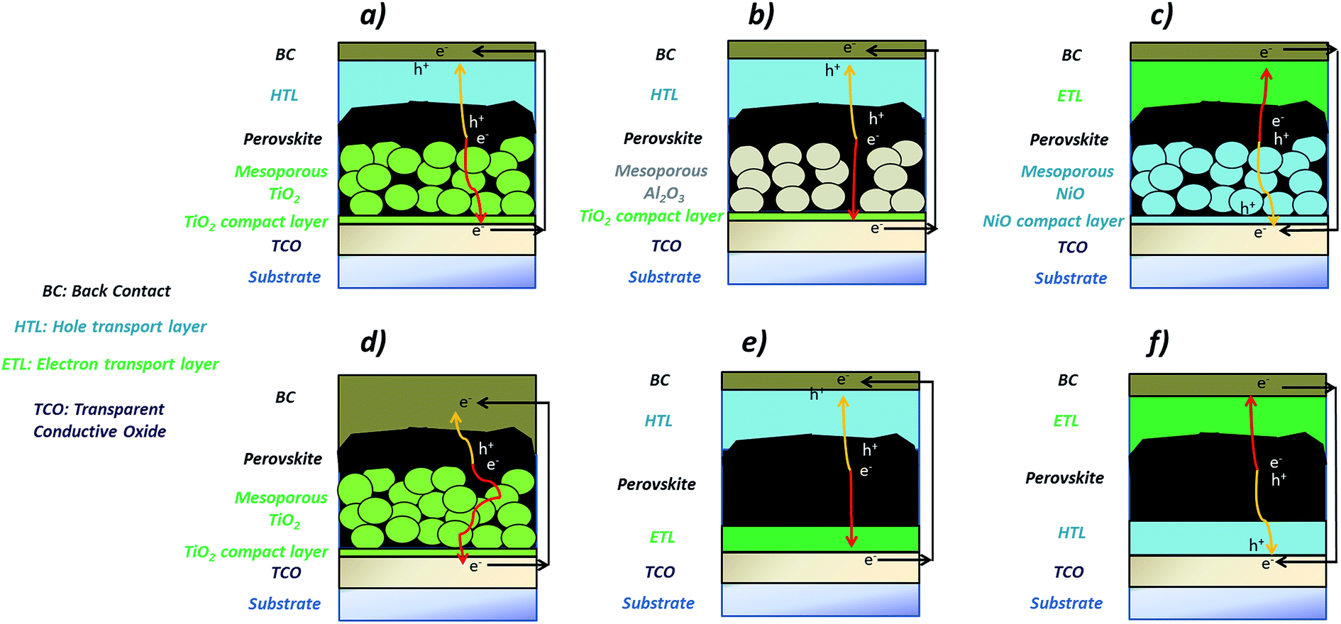 | ||
| Fig. 2 Perovskite solar cell architectures: (a) n-type TiO2 mesoporous-based; (b) insulating mesoporous-based; (c) p-type NiO mesoporous-based; (d) HTM-free mesoporous-based; (e) planar “n–i–p”; (f) planar “p–i–n”. Illumination occurs from the substrate side. In all these cases, the substrate can be either glass or polymer foil. | ||
In the planar configuration, the perovskite “thin film” is sandwiched between the selective transport layers. Since the sequence in which the layers are deposited can be reversed, the planar configuration is further sub-categorised into “n–i–p” and “p–i–n” configurations (Fig. 2e and f). In the former, the semiconducting TiO2 is deposited first, and acts as the n-type ETL, while the p-type layer (HTL) is based on the same organic materials employed for the mesoscopic architectures.38 In the “p–i–n” structure, both selective contacts are typically organic materials, such as PEDOT:PSS (HTL) and PCBM (ETL),39 although metal oxides have also been investigated. In each of these cases a TCO and a metal back contact complete the devices. Similar planar structures have been developed also by depositing methylammonium lead iodide, and intrinsic and doped organic charge transport molecules by vacuum processes.40 Recently, these devices have shown efficiencies comparable to devices based on solution processing, highlighting an effective alternative route to fabricate perovskite devices.
Despite the outstanding progress achieved in the past few years, several challenges have to be addressed in order to create a mature PV technology ready for commercialisation. Alongside the environmental concern related to the presence of lead,22,41,42 and the necessity to fully understand the hysteretic behaviour during current–voltage (I–V) measurements,43–46 there are significant efforts toward the improvement of efficiency, stability, device configuration and scalability of reproducible layer processes.47
In particular, the control of the complex (often 3D) interfaces in the PSCs and the related charge transfer and recombination processes plays an important role in achieving high performance solar cells. Moreover, the fabrication processes for the several materials used in the different architectures must be scalable and reproducible over large areas. In parallel to this, the understanding of the poor shelf-life and stability under thermal, light and humidity stress-testing of the PSCs remains at the forefront of research interest, together with the development of appropriate solutions.
3. ALD for perovskite solar cells
3.1. Electron and hole transport layers: requirements
The electron and hole transport layers have multiple roles in perovskite solar cells, namely: (i) to selectively extract charge carriers, whilst simultaneously blocking their counterpart, through the appropriate selection of their energetic levels; (ii) to minimize carrier recombination at the interfaces between the electrode and the transport layer and between the transport layer and the perovskite; and (iii) to be electrically continuous in order to reduce the presence of short-circuit (or shunt) pathways.Ensuring a correct alignment of the energy levels of the selective interlayers with the perovskite absorber is paramount to prevent energy barriers at the interface which may significantly hinder carrier extraction.48Fig. 3 shows an overview of metal oxides and organic materials (mostly inherited from DSC and OPV technologies) which are typically adopted in the various configurations due to their n-type (on the left in Fig. 3) or p-type behaviour (on the right).
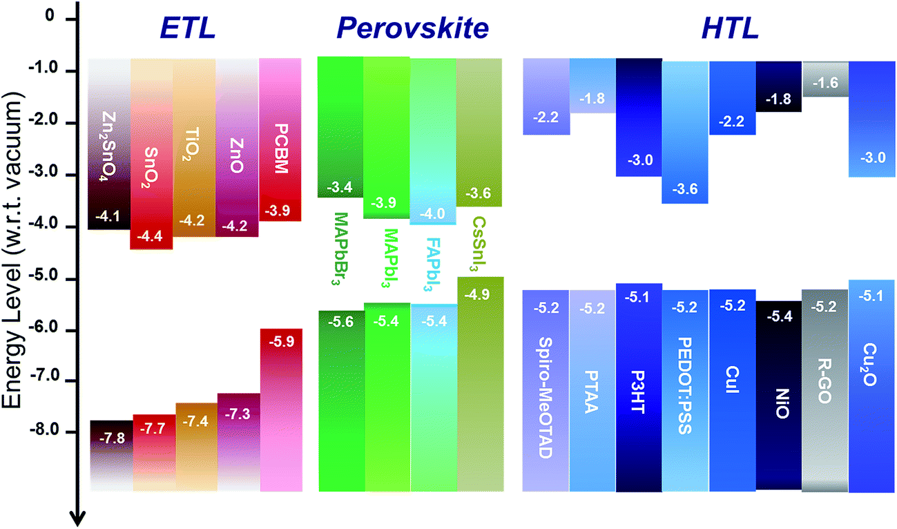 | ||
| Fig. 3 Illustration of literature values for the energy levels with respect to the vacuum level of different materials which act as electron-selective (left), perovskite absorber and hole-selective layers (right) in perovskite solar cells. These are the most commonly reported values in the literature (although they are spread over a wide range) and might change according to the deposition methods and post-deposition treatments. | ||
As a necessary condition, an electron transport layer should have a conduction band (CB) aligned with or slightly lower than the one of the absorber. A hole transport layer should have a more shallow valence band (VB), with respect to the VB of the perovskite. As well as this, the conduction band minimum and valence band maximum positions should be appropriate to enable or block carrier transport effectively as desired.
According to the literature, among n-type metal oxides, TiO2, ZnO, Zn2SnO4 and SnO2 exhibit appropriately aligned conduction bands (with respect to the CB of the perovskite), and deep valence bands to correctly extract electrons and block holes. Among the p-type layers, NiO has been taken into consideration according to its aligned valence band and shallow conduction band to correctly extract holes and to block electrons, respectively. Note that the exact Fermi-level position, and hence the work function, can be tuned significantly depending on deposition methods, and the use of post treatments.49–51 Elsewhere copper oxide52 and graphene oxide have also been tested as possible inorganic metal oxide HTLs.53 Furthermore, despite being n-type, MoO3 has been largely used in OPV configurations and it is being also explored in crystalline solar cells as an HTL material, since its very deep conduction band lends it a sufficiently high work function for hole extraction.54–57
Ideally, these selective contacts have to exhibit excellent electrical properties in order to maximize the charge collection and to minimize the contribution to the series resistance of the full device. These layers can be optimised by reducing their thickness, and/or increasing the conductivity (i.e. high mobility and/or high carrier concentration) of the films. Pristine Spiro-MeOTAD shows low hole mobility (1 × 10⁻⁵ to 1 × 10⁻⁴ cm2 V−1 s−1), and therefore, it is typically doped with a lithium salt, tert-butyl pyridine (TBP) and cobalt complexes.58 Decreasing the thickness of the PCBM layers in p–i–n architectures is an effective strategy to enhance the overall charge collection,59 and similar trends have been reported also for inorganic materials (i.e. NiO, TiO2, ZnO).60,61
ALD addresses these challenges, providing unrivalled film conformality. In the n-type mesostructured perovskite solar cells, the main role of the TiO2 compact layer (CL) is mainly to act as a hole blocking layer (HBL), since the electron extraction and collection are provided by the mesoporous TiO2 layer (see Fig. 2a). This TiO2 HBL/CL has to cover the TCO surface which would otherwise be in direct contact with the perovskite due to the mesoporous TiO2 film. Wu et al. demonstrated that a TiO2 ALD process (see Table 1 for ALD process details) generates very dense layers (50 nm) over FTO/glass substrates, yielding higher device performance (12.6%) than when conventional processes, such as spray pyrolysis or spin coating, were used (8.8% and 6.5% respectively).65 Similarly, we have shown that plasma-assisted ALD of TiO2 is an effective approach on ITO/glass,66 and also when working with temperature-sensitive ITO-coated polymer substrates for flexible mesostructured perovskite solar cells. In the last case, even, the high quality of the ALD deposited layer at low temperatures (150 °C) boosted cell efficiency to 9.2% (from 4% for conventional spin coating).67 Furthermore, plasma-assisted ALD layers have not only been successfully tested on small area samples (typical test lab 0.1 cm2), but also for the fabrication of a flexible sub mini-module with an active area of 8 cm2 (see Fig. 4).68
| Material | Metal precursor | Reactant | T substrate (°C) | Functional layer (architecture) | Ref. |
|---|---|---|---|---|---|
| TiO2 | TDMAT | H2O | 200 | Compact layer on FTO (mesostructured) | 65 |
| Ti(CpMe)(NMe2)3 | O2 plasma | 150 | Compact layer on ITO (mesostructured) | 67, 68 | |
| TTIP | O2 plasma | 100 | Compact layer on ITO (n–i–p planar) | 69 | |
| TDMAT | H2O2 | 120 | Compact layer on ITO (n–i–p planar) | 70 | |
| TDMAT | H2O | 150 | Compact layer on ITO (mesostructured) | 71 | |
| SnO2 | TDMASn | O3 | 118 | Compact layer on ITO (n–i–p planar) | 70, 72 |
| TDMASn | O2 plasma | 100 | Compact layer on ITO (n–i–p planar) | 73 | |
| ZnO | ZnEt2 | H2O | 70 | ETL on ITO (p–i–n planar and mesostructured) | 74 |
| ZnEt2 | H2O | 80 | ETL on PCBM (p–i–n planar) | 75 | |
| ZnEt2 | H2O | n.a. | ETL on Al2O3 nanoparticles (mesostructured) | 76 |
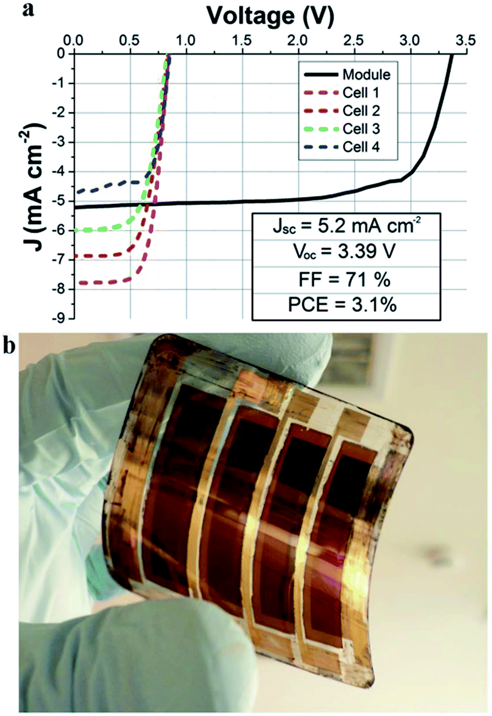 | ||
| Fig. 4 (a) Current density–voltage plot of an integrated flexible module made of 4 series-interconnected cells based on CH3NH3PbI(3−x)Clx with the PET/ITO/ALD-TiO2/TiO2 scaffold/perovskite/Spiro-MeOTAD/Au structure. Blue, green, red and magenta dashed lines are relative to the single cells while the continuous black line is relative to the module; (b) picture of the real device.68 Reproduced with permission from Adv. Energy Mater., 2015 Wiley. | ||
While for the mesostructured perovskite solar cells the superiority of the ALD TiO2 has been demonstrated in several studies, in the case of planar configurations the adoption of ALD led to contrasting results. High efficiency (12.2%) and hysteresis-free n–i–p planar devices were reported when using 20 nm plasma-ALD deposited TiO2 (deposited at 100 °C), whereas identical devices with solution processed TiO2 only reached efficiencies of 4.3%.69 The authors claimed that higher performance was related to the higher quality of the ALD TiO2 surface (fewer Ti3+ defects as detected by XPS and lower carbon investigated by FTIR) which led to faster charge injection at the interface with the CH3NH3PbI3−xClx perovskite absorber. On the contrary, low performance with plasma assisted ALD was reported in two other manuscripts.68,70 In our previous work, the planar architecture which included an 11 nm plasma assisted TiO2 compact layer (at 150 °C) showed high hysteresis in the JV curves and very poor efficiency (1–2%), primarily due to a low short-circuit current density (JSC). Although the layer showed excellent hole blocking properties, the poor performance was ascribed to the inefficient electron injection and collection toward the TCO.68
The poor injection at the TiO2/perovskite interface was described also in the work of Correa Banea et al.,70 where semicrystalline TiO2 was deposited at 120 °C on FTO–glass. In particular, the authors have shown that the hysteresis in the JV curves (Fig. 5a), the low stabilized JSC value (Fig. 5b), and the dependence of the photovoltaic parameters on the speed scan (Fig. 5d) are all consequences of a misalignment between the conduction band (CB) of the perovskite and the TiO2 (band offset, ΔEC, of 300 meV). The presence of this band offset creates undesired charge accumulation at the interface, and consequently the electron extraction becomes dependent on the scan rate during the measurements. Therefore, only when the device is held at a fixed potential, for instance, at the maximum power voltage (VMPP), the effective current density generated (JMPP) can be measured after a transient time (see Fig. 5b) and the overall efficiency can be determined.70
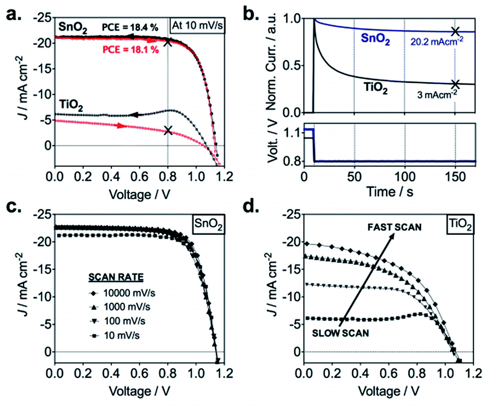 | ||
| Fig. 5 Photovoltaic characteristics of planar perovskite devices based on ALD SnO2 and TiO2 ETLs. (a) J–V curves of ALD TiO2 and SnO2-based planar mixed perovskite (FAPbI3)0.85(MAPbBr3)0.15 devices. The arrows indicate the scan directions; (b) normalized transient photocurrents measured from VOC to the maximum power point voltage for both planar systems; (c) scan rate (mV s−1) effects on J–V characteristics of ALD SnO2 and (d), ALD TiO2-based devices.70 Reproduced from ref. 69 with permission from The Royal Society of Chemistry. | ||
In contrast to the TiO2, the use of ALD SnO2 enabled to obtain high efficiency devices.70,73 Correa et al. reported the first use of this material via ALD, achieving a power conversion efficiency of 18% with no hysteresis effect (Fig. 4a) and no variation with the scan rate (Fig. 4c).70 The impressive result was ascribed to the deeper conduction band of the ALD SnO2, which facilitates the band alignment with the perovskite CB, consequently helping the electron extraction and avoiding any interfacial parasitic capacitive behaviour. The role of the band alignment in the electron extraction for the two different materials was successfully confirmed via femtosecond transient absorption (TA) measurements.70
We can conclude that a comprehensive understanding of the ETL/perovskite interface in terms of energy levels and their alignment is crucial for the optimization of the photovoltaic performance. Schulz et al.48 experimentally measured the valence and conduction band positions of TiO2, MAPbI3, MAPbI3−xClx, MAPbBr3 and Spiro-MeOTAD via ultraviolet photoemission spectroscopy (UPS) and inverse photoemission spectroscopy (IPES), in order to define the band offsets at the TiO2/perovskite and perovskite/Spiro-MeOTAD heterojunctions. They concluded that no significant band offset developed at the TiO2/perovskite interface (ΔEC of −100 meV), in strong contrast to that reported by Correa Banea et al. It is important to mention that several factors can affect the interface, starting from the quality of the TiO2 layer in terms of surface impurities, use of post-deposition treatments (UV-O3 exposure, O2 plasma), and sample handling and transfer in different processing environments (air, nitrogen). Furthermore, it has been already reported that the energy levels of the perovskite may be influenced by the substrate underneath, because of a substrate-dependent growth of the perovskite grain size crystals, and also by the density of defect states.77
The use of ALD ZnO was reported for the n–i–p planar configuration and also in the presence of an insulating scaffold. ALD ZnO generally exhibits high conductivity (with respect to ALD TiO2 and SnO2), and comparable energy levels to the TiO2; therefore it is considered an excellent ETL candidate. Relatively high efficiencies have been achieved (in the case of an insulating Al2O3 mesostructured architecture with 13.1%).74 However, its poor chemical stability when in direct contact with the perovskite compounds may limit its feasibility.
Elsewhere, in the p–i–n configuration, ALD ZnO has been deposited on top of the PCBM/perovskite stack. In this architecture, the ZnO acts as a buffer layer between PC61BM and the cathode to improve the contact properties with high work function metals (Au, Ag) which can be used in place of less stable low work function cathodes (i.e. Al and Ca). In this type of configuration, the adoption of ALD ZnO led to higher performance than for solution processed ZnO layers (respectively, 16% and 10%). The higher performance was ascribed to: (i) the higher uniformity of the ALD layer on top of the PCBM, thereby eliminating shunting pathways between the perovskite and the silver back contact and (ii) the higher electron mobility of the ALD ZnO layer.75
The high uniformity and conformality of ALD layers have also been explored for the deposition of ETL coatings within an insulating scaffold. This approach enables the simultaneous deposition of a continuous ETL extending through the Al2O3 mesoporous scaffold reaching the TCO surface underneath. Chandiran et al.76 demonstrated this concept by depositing ALD ZnO with thicknesses in the range of 1–6 nm, and achieving a maximum efficiency for 5 nm. With increasing the thickness of the ZnO layer further, the pore size decreased which reduced the ability of the perovskite absorber to infiltrate the scaffold structure, and consequently the performance worsened.
Among the other available p-type metal oxides, Cu2O and CuO layers have been recently deposited via solution processing in p–i–n perovskite based devices, reporting efficiencies up to 17–19%.91–94 Although direct application of ALD CuOx has not been reported yet, several ALD processes have been already developed.95–100
The potential of ALD in delivering doped metal oxides via a super-cycle approach (the dopant is generally introduced by alternating self-limiting growth of two binary oxide layers)4,106,107 has been widely investigated in the ALD community for the fabrication of TCOs based on ZnO (see Section 3.3). It is evident that the same approach can also be extended for a wide range of selective contact materials. ALD TiO2:Nb has been reported with interesting results, achieving similar electrical performance to the equivalent sputtered films.106 The combination of NiO and CuO (or Cu2O) ALD processes may be an interesting opportunity to fabricate doped HTLs.
In respect of the other deposition methods, i.e. solution-processing, the cyclic nature of the ALD process enables the introduction of doping materials with a high level of control. For example, the dopant can be uniformly distributed or a gradient can be generated in the bulk of the semiconductor, without any disruption in the layer continuity. Instead, in the case of solution processing, two different sequential depositions are required.
3.2. ALD for surface passivation
During the development of all PV technologies, the control and engineering of the properties of the multiple interfaces that are present in the various architectures play a fundamental role in delivering high efficiency devices. Whilst the combination of different materials is necessary for charge separation, in general any interface is a potential charge carrier loss region, at which higher defect densities typically exist with respect to the bulk. In crystalline silicon (c-Si) PV, the charge surface recombination processes are drastically reduced by the deposition of passivating ultra-thin metal oxides (i.e. Al2O3, SiO2). These materials either reduce the density of surface defects by saturating dangling bonds (i.e. chemical passivation), or repel minority charges away from the surface (i.e. field-effect passivation). ALD Al2O3 is nowadays industrially used in p-type PERC solar cells,108 and it has been reported as a strong candidate in n-type c-Si solar cells.109,110In TiO2 based mesostructured perovskite solar cells, the interface between the TiO2 nanoparticles and the perovskite (or between TiO2 and the HTM, in the case of high porosity of the absorber) can lead to undesired interfacial back charge transfer processes, as described in Fig. 6. These parasitic processes, which are driven by the surface states on the TiO2 nanoparticles, can be suppressed by the deposition of a metal oxide overlayer, similar to what was already adopted in DSSCs. In this latter case, a large variety of materials (TiO2, Nb2O5, ZrO2, Al2O3, MgO, Ga2O3, HfO2) have been successfully developed and deposited by sol–gel and ALD processes over μm thick mesoporous films.111–117 Since an efficient passivation layer must be pinhole-free, conformal on the TiO2 nanoparticles, and homogeneously distributed inside the mesoporous TiO2 layer, ALD is expected to meet these requirements. Nonetheless, a direct comparison between the solution processed and ALD methods has not been reported in the literature.
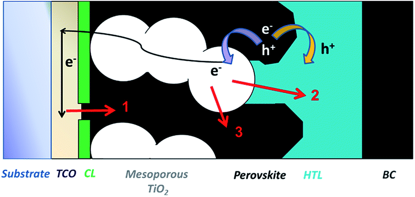 | ||
| Fig. 6 A schematic representation of an n-type TiO2 mesostructured perovskite solar cell. The arrows indicate the main recombination processes that can occur at the several interfaces: process 1 through defects in the compact layer deposited over the TCO/substrate; process 2 at the TiO2 nanoparticles/HTL layer interface in the case of direct contact between the two materials due to defects in the perovskite overlayer; process 3 at the TiO2 mesoporous layer/perovskite layer interface. | ||
In the case of the PSCs, ALD TiO2 overlayers have been successfully deposited over mesoporous TiO2,118 as well as on TiO2 nanorods,119 and the role of the ALD thickness (0–5 nm) was investigated (details of the processes are given in Table 2). In both studies, the optimal device performance was achieved using an ultra-thin overlayer (2 nm for the mesoporous layer and 5 nm for the nano-rod film) which is shown to passivate the TiO2 surface defects. Increasing the overlayer thickness led to a decrease of the photovoltaic performance, and this was explained by the reduction of the perovskite pore filling in both 3D structures, and by the amorphous nature of the thicker TiO2 overlayer which hinders the electron collection.118,119
| Material | Metal precursor | Reactant | T substrate (°C) | Functionality | Ref. |
|---|---|---|---|---|---|
| TiO2 | TDMAT | H2O | 120 | Passivation over FTO and mesoporous TiO2 | 67 |
| TTIP | H2O | 250 | Passivation over FTO and nanorod TiO2 | 68 | |
| Al2O3 | TMA | H2O | 100 | Passivation over compact layer and mesoporous TiO2 | 120, 121 |
| H2O | n.a. | Passivation over compact layer | 122 | ||
| H2O | 100 | Passivation on MAPI | 125 |
The use of wide band gap materials (i.e., Al2O3, SiO2, MgO, HfO2) as passivating layers introduces highly insulating energy barriers in both the conduction and valence bands between the perovskite and selective transport materials. Charge transport across these energy barriers is expected to proceed via tunnelling and so, these layers should be no thicker than the sub-nanometer range (tunnelling probability is significantly reduced for wider potential barriers). This has been proven in the case of DSCs,111,117 and clearly the sub-nanometer thickness control of ALD has lent itself to be an ideal technique for such passivation layers.
Although the nature of the perovskite absorber is deeply different from the one of the dye molecules, the same behaviour has been observed when an ALD Al2O3 overlayer was adopted to passivate the TiO2 mesoporous film. We observed efficiency enhancement upon depositing only 1–2 ALD cycles (η increased by 30%, and VOC increased by 100 mV) whereas increasing the number of ALD cycles to 5 and 10 led to a drastic reduction in JSC, and consequently in efficiency. This behaviour was explained by the inefficient electron extraction at the perovskite (MAPbI3)/Al2O3/TiO2 nanoparticle interface.120,121
A contrasting result was reported however by Lee et al.,122 who showed that already 1 ALD cycle of Al2O3 worsened the device performance. These results point out that the role and effect of the ALD layer on the interfacial charge transfer processes in the same architecture are not univocal, and will depend on the effective deposition thickness after 1 or a few ALD cycles and the quality of the ALD layer, which is dependent on several ALD processing parameters (precursor and co-reactant exposures, temperature), as well as the quality of the other device components: the TiO2 compact layer, the TiO2 scaffold and the perovskite absorber (note that in the two studies mentioned above the perovskite synthesis step was different). In the same work, the authors investigated the introduction of the ALD Al2O3 as passivation layer also on the surface of the TiO2 compact layer. 6 ALD cycles of Al2O3 were found to be advantageous when applied to passivate the TiO2 compact layer before the deposition of the mesoporous TiO2 film, whereas no benefit could have been observed for the planar n–i–p configuration (no mp-TiO2).122
As well as Al2O3, other ultra-wide band gap materials such as HfO2, ZrO2, MgO, and Y2O3 may be considered to be suitable passivation layers that can be deposited by ALD. MgO and Y2O3 in particular have been successfully applied in the mesostructured perovskite architecture via solution processing, yielding higher performance compared to the pristine samples.123,124
The accurate control of the deposited thickness offered by the ALD method has also been exploited to passivate the back surface of the perovskite layer in configurations without a hole transport layer (HTL free), i.e. whereby the perovskite is directly contacted with Au. In the absence of an electron blocking behaviour of the HTL, Wei et al. showed that 5 cycles of ALD Al2O3 can effectively suppress the electron transfer from the perovskite absorber to the Au electrode, and thereby improve the charge collection which leads to both higher JSC and VOC.125 Although no other studies have been published yet on this topic, the passivation of the perovskite absorber appears relevant for having highly efficient PSC devices. Indeed, in the p–i–n planar configuration it has been demonstrated that the PCBM layer, which is used as an efficient ETL, is also able to passivate trap states (i.e. dangling bonds at the top surface and along the grain boundaries) in the perovskite layer, leading to an improvement of the electronic properties of the absorber and eliminating the hysteresis in the IV measurements.126 The researchers used thermal admittance spectroscopy (TAS) analysis to quantitatively measure the trap states density reduction after the PCBM deposition, and after the optimization of the PCBM annealing step. Furthermore, they investigated the device under operating conditions (polarizing the solar cells under illumination) by means of the impedance spectroscopy (IS) technique. Their analysis revealed that the surface electron lifetime increased upon thermal annealing of PCBM, whereas the bulk lifetime remained constant. The same authors believe that there is room for further improvement of the performance by a more sophisticated surface passivation technique. Clearly, the accurate control of ALD processes has the potential to address this challenge, provided that the chemical compatibility of the chosen metal oxide processes with the perovskite is guaranteed, together with the identification of the appropriate passivation requirements in terms of effective thickness, material properties, and whether the passivation is required throughout the entire stack (e.g. by also passivating grain boundaries) or on the top surface only. Whilst in the example of Wei et al., ALD Al2O3 was successfully reported in the HTL-free architecture, no information has been reported about the interaction of the Al2O3 with the perovskite or whether the layer is distributed inside the perovskite layer.
Other ALD materials with similar dielectric behaviour to Al2O3 (i.e., HfO2, Ga2O3, MgO) can be tested. Furthermore, since the n-type PCBM acts simultaneously as passivation and electron transport layers, it might be worth investigating whether ALD ETL and HTL deposited on top of the perovskite would provide the same dual role. In Section 4, we will pay attention to the compatibility of Al2O3, TiO2, ZnO, NiO and MoOx ALD processing with the perovskite, providing an initial guidance for systematic research on this topic.
3.3. Solar cell tandem applications: recombination layers and TCOs
Perovskite solar cells are rapidly becoming the primary candidate for the wide band-gap top cell in tandem PV solutions, which in themselves are a burgeoning new focus of the PV community in view of reaching efficiencies exceeding 25%. The perovskite top-cells are to be paired with low band-gap bottoms cells such as c-Si or CIGS. Two configurations as displayed in Fig. 7 have been proposed: (a) the 4-terminal tandem, whereby two individual solar cells are fabricated separately and mechanically stacked but electrically isolated; and (b) the 2-terminal tandem, in which the top-cell is deposited directly on the bottom cell (usually Si or CIGS) and the two are monolithically connected. Some experimental examples on small area devices (<1 cm2) thus far demonstrate stable efficiencies of up to 22.8% (perovskite/Si, monolithic),127 and 20.5% (perovskite/CIGS, 4-terminal),128 and potential efficiencies over 30% have been predicted.129,130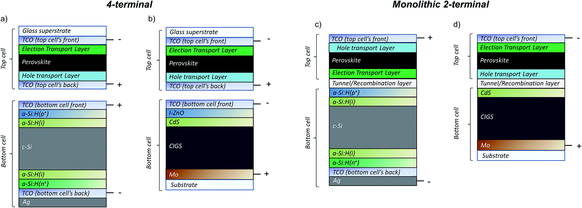 | ||
| Fig. 7 Schematics of the most investigated tandem solar cell configuration: perovskite/silicon heterojunction (SHJ) or perovskite/CIGS; in (a and b) 4-terminal, (c and d) 2-terminal architecture. The illumination occurs from the top cells. | ||
Alongside the optimisation of the perovskite band-gap,131 and the replacement of the metal electrode (i.e., Au, Ag, Al) with a transparent conductive electrode,132 a number of technical challenges remain for the tandem design. In both configurations, maximising the red to infrared (IR) transmittance through the entire top cell is paramount, since it is in this spectral region that the bottom cell operates (approximately 800–1150 nm, depending on the optimized band gaps of the perovskite and bottom cell respectively). In the specific case of the 2-terminal configuration, additional challenges include: (a) engineering of the tunnel/recombination layer between the two sub-cells; (b) ensuring that the bottom cell design does not restrict the processing of the top cell (for instance, solution deposition processes may not be optimal on textured c-Si cells); (c) eliminating process induced degradation of the bottom cell; and (d) matching the individual photocurrents of the sub-cells. We believe that the benefits of ALD can provide solutions to each of these issues.
Efficiencies for both tandem configurations are primarily limited by the parasitic absorption in the top cell in the UV, visible and near infrared (IR) spectral regions. Several studies demonstrated that this current loss is due to the light absorption occurring in the TCO and the organic HTL, such as Spiro-MeOTAD.130,132
Either in the 4- and 2-terminal cases, TCOs are adopted as electrodes, based on heavily doped metal oxides such as FTO and ITO. Their high carrier concentrations (1020 to 1021 cm−3),133,134 and subsequent poor IR transmittance are not problematic for the perovskite absorbers since the latter is not sensitive to wavelengths exceeding 850 nm. However, in tandem devices the significant free carrier absorption is highly limiting to the Si or CIGS bottom cell photocurrent, and in 2-terminal configurations, to the overall device current owing to their current-matching nature. For this reason, low carrier density and high mobility TCOs should be favoured for both front and back contacts in the case of 4-terminal, while in the 2-terminal configuration, high lateral conductivity is required only for the front contact. It is worth noting that in the latter configuration, the presence of the TCO is not limited to the front contact, but it is currently used also as a part of the tunnelling/recombination region between the sub-cells, and therefore parasitic absorption might arise also from this contribution.
Reported examples of tandem configurations thus far have used sputtering for TCO depositions. Werner et al.135 demonstrated 21% on a small area in 2-terminal monolithic perovskite/silicon heterojunction (SHJ) tandem solar cells using IZO as the intermediate recombination layer and an In2O3:H/ITO stack as the front contact. In the case of 4-terminal configurations, the TCO top front contact is typically commercially available FTO (TEC-15), while sputtered ZnO:Al136 or In2O3:H128 has been used as the top cell back contact. The electrical properties of the sputtered layers utilized in the literature are also reported in Table 3. Among the ALD TCO layers that can be deposited at low temperature (100 °C), only In2O3:H exhibits equivalent electrical performance,137 while ZnO:B exhibits an almost 60 times higher resistivity value (see Table 3). The ALD In2O3:H layer, when post-annealed at 200 °C, can offer a remarkably high μ (140 cm2 V−1 s−1) and lower n (1.5 × 1020 cm−3), resulting in a lower ρ (2.8 × 10⁻⁴ Ω cm) and significantly lower IR Drude absorption,137 making it an ideal candidate for both contacts of the perovskite top cell. However, the post processing at 200 °C temperature limits its application as a top cell front contact, but it can still be used as the intermediate recombination layer deposited on top of the SHJ solar cells, replacing the conventional ITO sputtered layer that is generally adopted.137 Alternatively, post annealing can be carried out at 150 °C to generate the same crystallization and the same electrical properties of the ALD In2O3:H layer, but at this temperature the annealing time is 10 times longer (from 10 min at 200 °C to 100 min at 150 °C).138
| ρ (mΩ cm) | [ne] (1020 cm−3) | μ (cm2 V−1 s−1) | Thickness (nm) | R sheet (Ω □−1) | T substrate (°C) | Ref. | |
|---|---|---|---|---|---|---|---|
| Sputtered IZO | 0.83 | 1.4 | 49 | 120 | 69 | 60 | 139 |
| Sputtered In2O3:H | 0.39 | 3.1 | 51 | 149 | 26 | 25 | 128 |
| Sputtered ZnO:Al | 2.2 | n.a | n.a | 400 | 55 | n.a. | 136 |
| Sputtered ITO | 0.5 | n.a | n.a | 500 | 10 | 25 | 140 |
| ALD In2O3:H | 0.35 | 4.6 | 50 | 75 | 47 | 100 | 137 |
| ALD ZnO:B | 20 | n.a | n.a | 75 | 2670 | 100 | 4 |
Additional parasitic absorption in the top cell generates from the Spiro-OMeTAD HTL layer, which is generally used since it delivers the highest efficient single junction device. This is particularly evident in the monolithic configuration, due to the fact that the illumination comes from the side of the Spiro-OMeTAD layer. Indeed, this material exhibits a large absorption throughout the range of 300–1200 nm,132 and therefore its replacement with HTLs that have low UV and IR absorption should be pursued. As discussed in Section 3.2, NiO is a potential candidate, being a wider band gap material which was already adopted as a HTL in p–i–n perovskite cells. Obviously, the reduction of the HTL thickness can minimize the parasitic absorption, and whereas there are practical limitations for reducing the thickness of solution-deposited organic HTL materials, this is not an issue for layers prepared by ALD.
Next to the parasitic absorption, a further limitation induced by the presence of the Spiro-OMeTAD that has been reported thus far is the sputtering damage during TCO deposition. In order to mitigate this effect, the use of buffer layers such as thermally evaporated MoO3,139 ITO or ZnO:Al nanoparticles131,140 has been adopted prior to the TCO deposition. Indeed, Werner et al.139 demonstrated that the direct deposition of IZO on top of the Spiro-MeOTAD is detrimental for the FF as the sputtering power is increased from 60 W to 200 W, and the presence of a thermally evaporated MoOx buffer layer (10–35 nm) is required to mitigate this damage. It is worth noting that also the MoOx can be affected by sputtering processes, modifying the absorption response of the material inducing parasitic absorption in the visible region when used in the device.141 Therefore, low plasma power for the sputtering process is still desired although this condition leads to TCO with higher sheet resistance (Rsheet).139 These problems would be less relevant in the case of the ALD process involving H2O as an oxidant agent (such as the ALD process for ZnO and In2O3:H), since no high energies are involved during the deposition.137,142
In the 2-terminal configuration, the sub-cells are electrically connected via a tunneling/recombination layer. The general term of ‘tunneling/recombination’ layer is used here since at the current state of research the monolithic connection proceeds via quantum tunnelling, conduction-to-valence band recombination of the photogenerated carriers, or a multi-step tunnelling mechanism, depending on the type of tandem architecture.143 In the case of a SHJ bottom cell, the tunnelling/recombination layer is based on the a-Si:H (p+)/TCO/ETL stack. Low temperature processing (<200 °C) as well as ‘soft’ deposition methods should be selected in order to prevent the reduction of the passivation at the c-Si/a:Si:H(i) interface with a consequent decrease of the PV performance. For instance, ALD TCO (e.g. ZnO:Al) on a c-Si heterojunction (SHJ) has already been investigated for the generation of front contacts, and the ALD process was shown to provide greater protection (compared to a sputtered ITO-process) to the passivation properties of the underlying a-Si:H(i) layer.142 An innovative low temperature ALD MoO3/In2O3:H stack has been proposed to replace the p-doped a:Si:H/sputtered ITO, with encouraging results to maintain excellent passivation properties of the c-Si/a:Si:H(i) interface.144 Furthermore, the conventional electron transport layer used in the perovskite solar cells, such as the mesoporous TiO2 film and/or spray pyrolysis compact TiO2, are not compatible with SHJ, since they require high sintering temperature (450–500 °C). Albrecht et al.72 reported the adoption of a low temperature (120 °C) ALD SnO2 layer as the ETL, deposited on sputtered-ITO, achieving an 18.1% efficient perovskite/Si device. These examples highlight how a potential stack of three low temperature ALD layers (MoO3/In2O3/SnO2) may be investigated in the perovskite/SHJ tandem configuration. Similar constraints regarding processing temperature and TCO deposition methods are reported in the case of the CIGS, where the recombination stack is generally composed of CdS/TCO/HTL layers.145 In this case, the fabrication of an efficient recombination layer can exploit all the efforts in replacing the conventional CdS/intrinsic ZnO/stack with ALD ZnO based layers, such as Zn(O,S) and Zn1−xMgxO.146–149 The sputtered AZO generally used as TCO in CIGS might be replaced by ALD TCOs such as In2O3:H or ALD doped ZnO such as ZnO:B,4 ZnO:Ga,150,151 if low temperature (<200 °C) ALD processes enable sufficient electrical properties. The organic PEDOT:PSS, which has been used as a HTL in the work of Todorov et al.,145 can be replaced by low temperature ALD NiO or CuOx as we discussed in Section 3.2, potentially providing a complete ALD stack (i.e., Zn(O,S)/ZnO:B or In2O3:H/NiO).
For a monolithic configuration employing a SHJ as the bottom cell, recently Werner et al.152 pointed out that using a double-sided textured silicon wafer would enable to enhance the bottom filtered SHJ current density with respect to the case where a double polished or rear side textured wafer has been used. In the case of deposition on textured c-Si, the unrivalled conformality of ultra-thin ALD films provides similar electrical continuity advantages to those outlined in Section 3.1 and 3.2. This conformality is well exemplified by the application of thermal ALD Al2O3153 or plasma assisted ALD Al2O3/SiO2,154 on top of highly textured ‘black-Si which is also shown in Fig. 8.
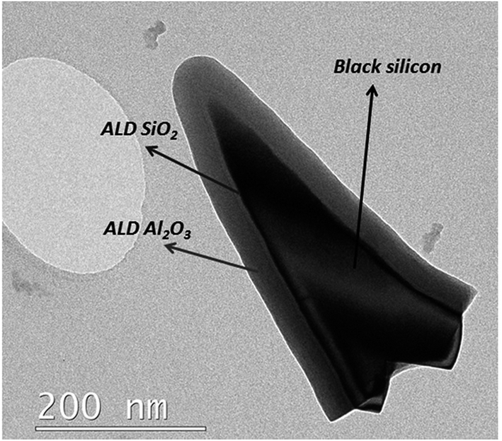 | ||
| Fig. 8 TEM image of a black silicon pillar taken from the surface of the wafer coated with 4.4 nm SiO2 and 30 nm of Al2O3via a plasma assisted ALD process. | ||
As well as recombination layers, there are efforts to incorporate optical splitters at the regions between top and bottom cells,155 which may be served by plasmonic metallic structures, such as those shown by Zhang et al.156 These structures can also be deposited by a high level of control by ALD.157
Finally, we discuss the opportunities for novel ‘dielectric-metal-dielectric’ (DMD) structures, which can provide an alternative route towards obtaining highly transparent and conductive materials, which could equally be incorporated as transparent back contacts in tandem solar cells. Typically, metal oxide layers (on the scale of 10 s of nm) sandwich an even thinner (<10 nm) metal layer which provides lateral conductivity. Recently, Yang et al.158 developed a semi-transparent top electrode based on MoOx/Au/Ag/MoOx, which was adopted in a 4 terminal perovskite/CIGS tandem solar cell. The optimization of the DMD structure requires very thin layers (10 nm/1 nm/10 nm/40 nm) in order to achieve satisfactory electrical conductivity and sufficient transparency in the visible and near IR region spectra.158 Whilst thermal evaporation was used for generating the complete stack, the accurate control in thickness for either metal-oxides and metal particles by ALD might generate improved results, and especially in the case of textured substrates such as c-Si bottom cells, it will be an interesting route to be explored.
3.4. ALD for perovskite encapsulation
Next to the improvement of single active device layers, the fabrication of perovskite solar cells having adequately long-term operating lifetimes for their intended end-use remains a major challenge. Perovskite devices are known to be highly susceptible to deterioration, and this has been linked to both extrinsic (oxygen, light, moisture and temperature) and intrinsic (device interfaces and species diffusion) factors.159–165 In terms of extrinsically induced degradation, several mechanisms lead to the decomposition of the perovskite crystalline structure into its components, mainly PbI2, hydrogen iodide (HI) and organic compounds. The possible decomposition paths and the role of the specific extrinsic factors in inducing device degradation are still under discussion and detailed descriptions of these mechanisms are extensively reported in the reviews by Niu et al.166 and Berhe et al.159 In order to improve the absorber layer intrinsic stability, three main approaches have been reported: (i) the substitution of the pure iodide (PbI3) with a mixture (PbI3−xBr,Clx) of halides, which has been proven to induce structural phase variations;167 (ii) modification of the organic cation (e.g. replacing methylammonium with formamidinium) or using a mixture of different organic cations168 (iii) use of an all-inorganic perovskite structure, substituting the organic ligand with inorganic materials (e.g., Cs).169The overall stability of the device has been demonstrated to be poor using organic ETLs and HTLs.78,170 The organic layers have been found to influence the device shelf-life, since they poorly protect the perovskite layer against the ingress of moisture and oxygen, and they are susceptible to degradation themselves. Indeed, the replacement of PEDOT:PSS and PCBM in the p–i–n configuration with metal oxides (NiO and ZnO) largely extends the lifetime of the devices.78,105 In the TiO2 based mesostructured perovskite solar cells, the dopants used in the Spiro-MeOTAD significantly affect the stability of the devices. Organic layers and their interfaces with the perovskite absorber also appear to have a strong effect on the deterioration of the device performance, and long term stability has not been achieved.163,171,172 Therefore, next to the doped HTL-free,173,174 also the complete removal of Spiro-MeOTAD and the adoption of carbon based electrodes were demonstrated as a valid strategy to extend the device stability.36
The adoption of hydrophobic tunnelling insulating layers deposited on top of the perovskite has been proven to enhance the air stability of perovskite solar cells.175 Similar behaviour is observed for the first time also using an ultrathin ALD Al2O3 layer (nominally 0.8 nm) deposited at 100 °C on top of the perovskite absorber.176 For long-term stability however, the application of permeation barrier layers against water and moisture ingress (see Fig. 9) and the replacement of organic materials with metal oxides60,78,177 appear necessary. While the adoption and the opportunities of ALD inorganic layers have been discussed in Section 3.2, this paragraph will focus on the possibility that ALD offers to deposit ultra-thin, virtually pinhole-free layers acting as moisture barriers, exploiting also the experience demonstrated for direct deposition of barriers on temperature sensitive devices such as organic LED and OPV technologies.178–180 The barrier properties of a thin film related to the permeation through the nano-pores are generally addressed as intrinsic, while the overall barrier quality through both macro-defects and nano-pores is addressed as effective.‡ Generally, effective water vapor transmission rate (WVTR) values are typically obtained in the range of 10−4 to 10−6 g per day per m2. As a reference, a WVTR in the order of 10−6 g per day per m2 is required in order to ensure a long lifetime (i.e., >104 h) for an organic LED, which is considered the most demanding technology in terms of water/oxygen susceptibility. Typically, OPV devices need barriers with a WVTR value in the order of 10−4 g per day per m2.178–180 Although specific values are not reported for the perovskite technology, providing similar values by using compatible deposition processes is highly desired. In Table 4, a summary of the best low temperature ALD layers in terms of barrier properties is reported.
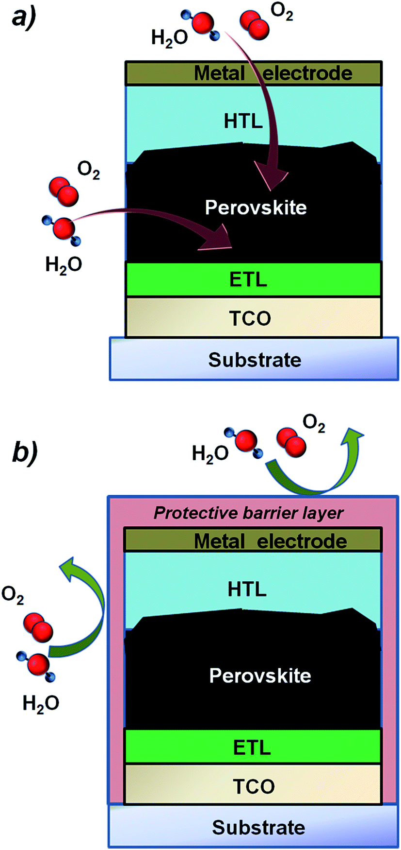 | ||
| Fig. 9 Schematic of a perovskite solar device with and without a protective barrier layer against moisture and O2 which are responsible for the degradation of the perovskite thin films and the interface with the selective contacts (ETL and HTL) and electrodes. | ||
Plasma assisted ALD single inorganic barrier layers have been shown to give outperforming results in terms of both intrinsic and effective barrier performance; in particular, for the effective water vapor transmission rate (WVTR) a value of 5 × 10⁻⁵ g per day per m2 (T = 38 °C, RH = 85%) was reported by Carcia et al.181 for an ALD Al2O3 layer of 10 nm grown on a polyethylene naphthalate (PEN) substrate, deposited at 125 °C. A lower deposition temperature (80 °C) is reported for spatial-ALD of TiO2 where the effective c WVTR values of 5 × 10⁻⁴ g per day per m2 (T = 38 °C, RH = 90%) were measured for 20![[thin space (1/6-em)]](https://www.rsc.org/images/entities/char_2009.gif) nm-thick layers.182 In terms of intrinsic WVTR, values of 1 × 10⁻⁶ g per day per m2 (T = 20 °C, RH = 50%) have been reached with a 20 nm plasma assisted-ALD Al2O3 single layer deposited not only at 110 °C,13 but also at 25 °C.183 Recently, Andringa et al.184 reported that the deposition of a plasma assisted-ALD ultra-thin SiNx layer (10 nm) at 80 °C showed an intrinsic WVTR value in the order of 10−6 g per day per m2 (T = 20 °C, RH = 50%).
nm-thick layers.182 In terms of intrinsic WVTR, values of 1 × 10⁻⁶ g per day per m2 (T = 20 °C, RH = 50%) have been reached with a 20 nm plasma assisted-ALD Al2O3 single layer deposited not only at 110 °C,13 but also at 25 °C.183 Recently, Andringa et al.184 reported that the deposition of a plasma assisted-ALD ultra-thin SiNx layer (10 nm) at 80 °C showed an intrinsic WVTR value in the order of 10−6 g per day per m2 (T = 20 °C, RH = 50%).
Alongside the deposition of single inorganic layers, ALD gives the possibility to deposit nanolaminates (either inorganic or hybrid) as permeation barriers. In the literature, several combinations of Al2O3 with other metal oxides deposited by ALD have been reported, and selected examples are Al2O3/ZrO2 (<100 °C),178 Al2O3/HfO2 (100 °C),185 and plasma-assisted ALD Al2O3/TiO2 (<100 °C).186 Hybrid solutions have recently been reported adopting a combination of ALD and molecular layer deposition (MLD).187 In this technique, the conventional H2O, O3 or O2 plasma co-reactant is substituted with an organic molecule, for instance ethylene glycol or glycerol, which maintains the self-limiting nature of the ALD process, whilst allowing the deposition of different hybrid materials.188 Selected examples are Al2O3/alucone,189,190 and TiO2/self-assembled monolayers.191 Together with the excellent barrier properties of ALD layers, this technique has been shown to reduce the amount of local defects/pinholes that are generally induced by the process itself. The high conformality of the deposition process leads to a lower density of pinholes, thereby proving that the technique can also be effective for direct device encapsulation. For OPV devices, Chang et al.180 reported the direct ALD deposition of Al2O3 and nanolaminates of Al2O3/HfO2 and the variation of device performance and layer morphology as a function of the ALD process parameters (precursor soaking, process temperature and materials). Sarkar et al.192 investigated the effect of using different co-precursors (H2O and O3) on the efficacy of the OPV encapsulation adopting ALD Al2O3 as a barrier. Finally, Clark et al.193,194 reported a systematic study as a function of process parameters and the thickness of ALD Al2O3 on bulk heterojunction OPV devices, focusing on the ALD layer growth and its adhesion. For all these studies, ALD processes were carried out in the range of 80–120 °C.
With regard to direct application of ALD-encapsulation for perovskite solar cells, there are few reported examples in the literature that demonstrate an improvement of the device lifetime. ALD Al2O3 has been deposited on top of the HTL/perovskite system in order to limit the ingress of water and oxygen in the device.195 The deposition was limited to 3 cycles, in order to enable charge collection at the electrode, and a decrease in the device efficiency of only 10% within 24 days of air exposure was obtained, whereas the pristine device exhibited remarkable degradation of the photovoltaic parameters (no efficiency was reported). It is worth noting that the theoretical sub-nm thickness of the ALD layer is not sufficient to create a continuous film and, in turn, a suitable encapsulation layer. Nonetheless, the improvement in device lifetime highlights the promising role of ALD in the development of end-term perovskite technology.
Furthermore, Chang et al.75 reported an encapsulation strategy based on the deposition of 50 nm-thick ALD Al2O3 on a PET substrate which was then applied on top of the perovskite device. The WVTR reported is in the order of 10−4 g per day per m2 and the device has been tested for 40 days, showing minor deterioration of efficiency, in contrast to the pristine device which was not working already after only 10 days (see Fig. 10).
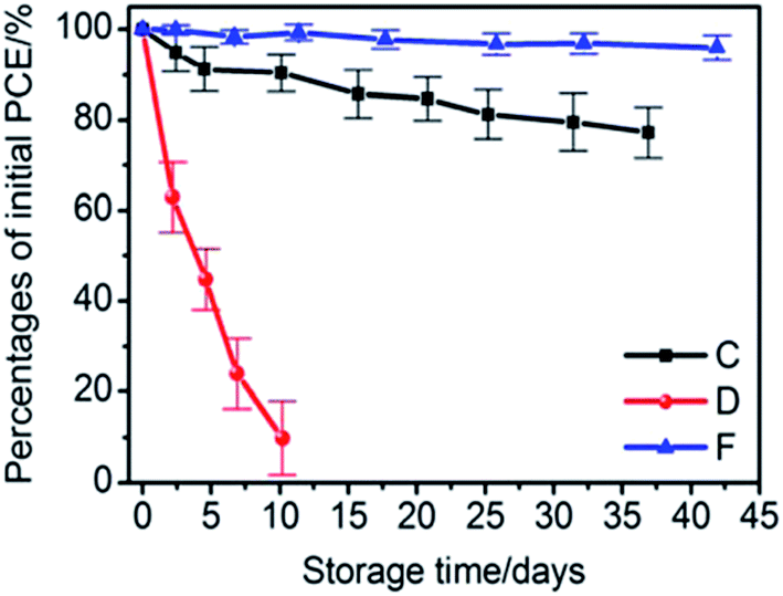 | ||
| Fig. 10 Percentage of the initial PCE as a function of storage time in an ambient atmosphere (30 °C, 65% relative humidity) for the perovskite solar cells with only a metal contact (red circle), semi-transparent back contact (black squares) and semi-transparent back contact in combination with ALD based indirect encapsulation (blue triangles). The error bars are calculated as the standard deviation from the mean value for a set of 25 devices.75 “Reprinted with permission from High-Performance, Air-Stable, Low-Temperature Processed Semitransparent Perovskite Solar Cells Enabled by Atomic Layer Deposition, Chem. Mater., 2015, 27, 5122, Copyright {2015} American Chemical Society”. | ||
4. ALD processing over perovskite layers – process development and compatibility
Since ALD was initially required in semiconductor industry applications, most ALD processes were developed and designed to be compatible with inorganic materials (semiconductors, metal oxides, nitrides, and metals),196–198 which exhibit far greater stability than is to be expected for organic or hybrid compounds during ALD processing. More demanding was indeed the application of ALD films on ultra-thin amorphous silicon layers (1–5 nm) for PV applications,142 and temperature sensitive materials such as polymers and textile substrates, where the constraints on the processing temperatures have required the development of low temperature (also down to room temperature) ALD processes.157,199Organic–inorganic hybrid metal halide perovskites are considered “soft materials”, which have been demonstrated to easily degrade when exposed to high temperatures, moisture, oxygen and UV light.159,200,201 The main consequence is the decomposition of the perovskite structures. It is reported that the degradation pathway and its extent differ with the type of perovskite (MAPbI3, FAPbI3, or mixed MAPbI3−xBrx, MAPbI3−xClx) and also its fabrication procedures (i.e. single or double step deposition methods).166,171,200
Most of the ALD processes for metal oxides, which can work as efficient functional layers in several perovskite configurations, have been developed in a wide range of temperatures (typically 100–400 °C) involving oxidative environments where water vapour or ozone is used as a co-reactant, so called thermal ALD processes. In order to decrease the processing temperatures, the plasma assisted ALD process can be utilized as well. In this case, water vapour or ozone is replaced by an O2 plasma exposure step (see Fig. 1).202
Next to the oxidant, the first half of every ALD cycle involves a metal precursor dose whose reactivity and the chemical interaction with the perovskite surface will play a key role in driving the growth of the metal oxide. Whilst ALD has been reported for the fabrication of layers over the TCO/substrates, (i.e. prior to the deposition of the perovskite), its application and the effect of the ALD process parameters directly on the perovskite have been rather unexplored. Some examples include the deposition of a few cycles of Al2O3 on MAPbI3 in two different studies.125,195 The layers (1–5 ALD cycles) were deposited at different temperatures (70 °C and 100 °C) using different oxidants (O3 and H2O), and their application led to contrasting results, with a reduction of the PV performance in the case of the deposition at 70 °C using ozone,195 and an enhancement of the efficiency when the deposition occurred at 100 °C employing H2O as a co-reactant.125 In another study, spatial atmospheric ALD ZnO was successfully deposited at 70 °C on top of MAPbBr3 for OLED application.203
In this section we investigate the compatibility and the response of the MAPbI3 perovskite (see experimental details in the ESI†) when undergoing prolonged temperature stress, different co-reactants and metal precursors. Although other perovskites such as CsxFA1−xPbI3−yBry and MAPbBr3 exhibit already a higher tolerance to elevated temperatures with respect to the MAPbI3,204,205 the latter one is by far the most commonly used in the PV research, and therefore it can be considered the best model system to explore. Hence, the aim of this study consists of elucidating the role of ALD processing parameters in the growth of the ALD layers, and at the same time providing useful insight with respect to the engineering of the ALD suitable processes for perovskite based solar cells. This study is carried out by means of ex situ XRD and surface XPS measurements. The XRD analysis will be presented as a comparison between the areas calculated for the two selected peaks in the XRD pattern measured for all the samples under investigation: the {110} peak of the MAPbI3 and the {001} peak of the PbI2. In the figures, these areas are normalized to the values of the pristine MAPbI3 layer. In the case of the XPS analysis, only selected elements will be displayed: nitrogen and iodine since they exhibit the most significant variations in the perovskite chemistry, and the elements related to the specific test carried out.
4.1. Influence of induced thermal stress on the perovskite layer
The response of the perovskite layer to the thermal stress under vacuum conditions (inside an ALD reactor) was first investigated. Samples were placed under low vacuum conditions (0.1–30 Torr) to simulate the same environment built up during the ALD processes and they were kept for 4 h at different temperatures (30–100 °C). Fig. 11a shows the XRD pattern for the pristine perovskite film prepared following the procedure of Qiu et al. (see ESI†),206 while Fig. 11b and 10c show the main peak at 14.1° associated with the {110} peak of the MAPbI3 and the one at 12.6° related to the {001} peak of the PbI2. The result of the XRD analysis is reported in Fig. 11d. We can observe that already a prolonged exposure at 100 °C leads to a variation in the perovskite, with a decrease of the selected peak of the MAPbI3 of almost 40%, while an increment of 6 times for the PbI2 contribution. The lower stability exhibited in our study with respect to the literature where MAPbI3 has been reported to be thermally stable up to 140 °C in nitrogen201 might be ascribed to the vacuum conditions and the prolonged exposure. Indeed, no effect has been observed after only 1 h at 100 °C (not shown here). Our result is in agreement with other reports, where it is highlighted that the thermal budget induces degradation of the organic methylammonium component to HI and CH3NH2 by-products, which sublimate and lead to the formation of PbI2.201,207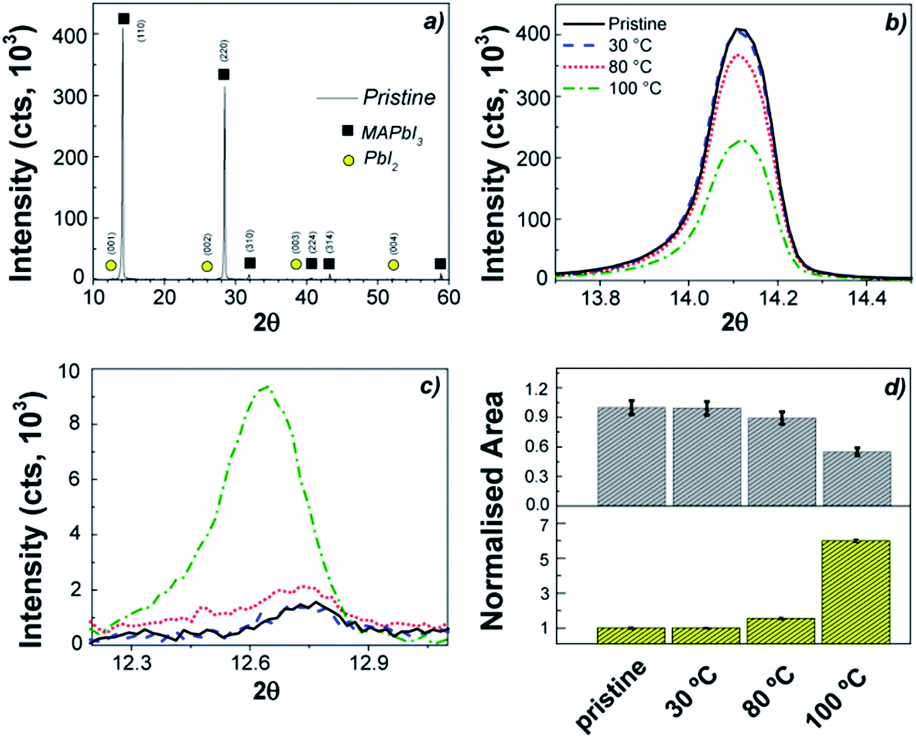 | ||
| Fig. 11 (a) XRD spectrum of the pristine MAPbI3 perovskite layer deposited on an ALD TiO2 film; (b) {110} peak of MAPbI3 for the pristine reference and the samples after 4 h at operating pressures (0.1–30 Torr) inside the ALD reactor, at 30 °C, 80 °C, 100 °C; (c) {001} peak of PbI2; (d) comparison of the normalized area of the main peak at 14.1° of MAPbI3 and the one for the PbI2 at 12.6°. | ||
As already mentioned, typical thermal ALD processes of metal oxides require temperatures in the range of 100–400 °C,202 and therefore it appears that the thermal budget that the MAPbI3 perovskite can withstand will be limited, indicating that ALD processing temperature and time should be minimized as much as possible. Spatial ALD processes can drastically reduce the ALD cycle time (and thus the length of the process) and they can potentially be used at lower temperatures than 100 °C.182,208–211 Alternatively, plasma assisted approaches enable processing temperatures below 100 °C, even down to room temperature, for several metal oxides (i.e. Al2O3, TiO2, MoO3 and NiO),3,202,212,213 as we will present in the following sections.
4.2. Influence of ALD co-reactants for metal oxide processing on perovskite layers
The stability of the MAPbI3 perovskite layer was verified also with respect to the oxidizing agent typically employed in the ALD processes for metal oxides. Generally, water vapour, ozone and oxygen plasma are employed to generate the M–O bonds, and their interaction with the perovskite layer might be deleterious for its stability. Indeed, the role of H2O, in particular from the moisture in the ambient, has been thoroughly investigated, highlighting the hydration mechanism which leads to the decomposition of the material in high humidity environments.159,200,201 Molecular oxygen (O2) from the environment, in combination with light and in the presence of photocatalytic TiO2 layers, induces the deprotonation of MAPbI3, resulting in decomposition into CH3NH2, PbI2, I2 and H2O.159The effect of the direct exposure of MAPbI3 to H2O and O2 plasma as investigated by XPS and XRD is reported in Fig. 12. H2O was dosed for 250 ms, while the O2 plasma was ignited for 3 s, in order to simulate the oxidizing half reaction of the corresponding ALD cycle. Both co-reactant exposures were repeated 50 times, with a purging step in between. With respect to the pristine perovskite layer, the degradation effect is evident for the direct exposure to the O2 plasma already at 30 °C. In particular, from the XPS analysis of the surface, the N1s peak associated with the N–C bond from the methylammonium (402 eV) totally disappears. Furthermore, the peak at 624 eV in the I3d spectrum and the detectable oxygen (O1s) at 532 eV reveal that the iodine oxidation process occurs upon O2 plasma exposure, leading to the formation of iodate species. In addition to that, the iodine peak associated with the I–Pb bond exhibits a shift towards lower binding energies, which can be explained by the less electronegative chemical environment created by the removal of the organic cation. Alongside the change on the perovskite surface, the main XRD peak of the perovskite reduces by almost 40%, in combination with an increase of the PbI2 peak (Fig. 12d). Contrary to this, no alteration in the chemical composition and the perovskite crystallinity occurs after H2O exposure at 80 °C (see Fig. 12). The absence of the oxygen peak indicates that the perovskite is not very sensitive to the oxidative environment created inside the ALD reactor during the sequential repetition of water vapour pulses, although the instability of this material under humid conditions is well known. However, the single pulse of H2O we have used in our study (250 ms) creates an environment with a maximum of 0.1% of relative humidity (RH), which is much lower than the large variety of conditions mentioned in the literature to degrade the perovskite.166,171,200 Therefore, this result looks highly promising for depositing layers by means of H2O based thermal ALD processes. A similar result was reported also by Choudhury et al.,214 where the dosage of consecutive H2O pulses (100 repetitions at 75 °C) led to only a very small variation in the optical properties of the mixed halide perovskite, MAPbI3−xClx.
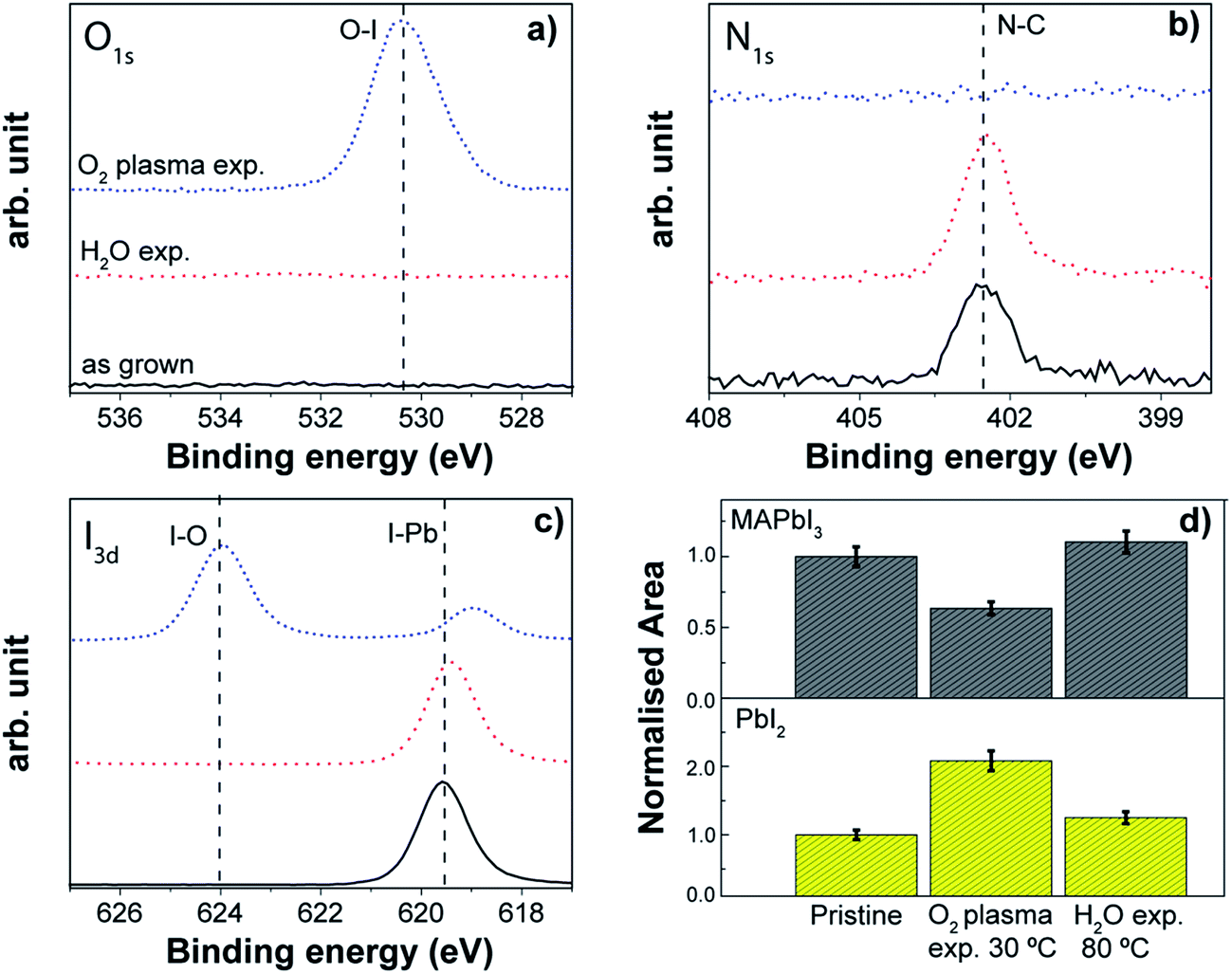 | ||
| Fig. 12 XPS spectra of (a) O1s (b) N1s and (c) I3d for the pristine, H2O-exposed (50 pulses at 80 °C) and O2 plasma-exposed (50 pulses at 30 °C) perovskite samples. (d) Normalized areas of the {110} peak of the MAPbI3 perovskite and {001} peak for PbI2. | ||
In contrast to the presented results and those of Choudhury et al., Kim and Martinson reported that the exposure of MAPbI3−xClx to H2O (15 ms of dosing, 100 times at 100 °C) led to a strong development of PbI2 according to their XRD analysis. As a consequence, they suggested the use of acetic acid as the oxidizing agent, which appeared not to induce perovskite degradation.215 The contrasting results can possibly be ascribed to the different intrinsic stability of the perovskites used in the three studies.
4.3. Comparing thermal and plasma assisted ALD processes for Al2O3
ALD of Al2O3 is considered a model system in the ALD community since it has been widely explored and applied. Therefore, we investigated both thermal and plasma assisted Al2O3 processes as case studies to evaluate the effect of a complete ALD process on the perovskite absorber. Although we are aware that the application of the Al2O3 might be limited to ultra-thin passivation layers over the perovskite absorber due to its dielectric behaviour (see also Section 3.2), these case studies can provide significant insights into the effect of ALD processing. Information about the processes is reported in Table S2.†A thermal ALD Al2O3 process at 80 °C enabled the growth of an Al2O3 layer on top of the perovskite surface as demonstrated by the detection of the Al peak at 74.6 eV in XPS analysis (see Fig. 13a). The process appears compatible with the organo lead iodide chemistry. Neither degradation/variation in the nitrogen spectrum nor changes in the iodine spectrum were observed. Only a slight increase in the PbI2 peak compared to the as-grown sample was discernible by the XRD investigation (Fig. 13d).
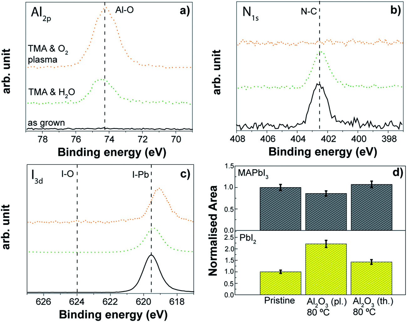 | ||
| Fig. 13 XPS analysis of three perovskite samples: pristine, upon thermal ALD Al2O3 at 80 °C and plasma-assisted ALD at 80 °C depositions. (a) Al2p (b) N1s (c) I3d. (d) Normalized areas of the {110} peak of the MAPbI3 and the PbI2 {001} peak. | ||
Also the plasma assisted process carried out at the same temperature (80 °C) allows the Al2O3 layer to grow on top of the perovskite, although some differences occur with respect to the thermal process. In particular, the nitrogen peak at 402 eV disappears after the Al2O3 growth (Fig. 13b), a shift towards lower binding energies of the iodine peak related to the I–Pb bond is discernible (Fig. 13c), and the crystallinity of the perovskite decreases with a slight increment of the PbI2 contribution (see Fig. 13d). This is somewhat expected given the higher reactivity upon the direct exposure to O2 plasma compared to the H2O exposure (see Fig. 12). Of great interest however is that the perovskite degradation during the complete ALD process is largely mitigated when compared to the direct O2 plasma exposure (see Fig. 12), which is particularly evident due to the absence of iodate formation (Fig. 12c with respect to Fig. 13c). The use of the complete ALD cycle based on the trimethylaluminium (TMA) and the O2-plasma leads to early saturation of the substrate with TMA and the subsequent Al2O3 growth is sufficient to shield the perovskite from damaging effects by the O2-plasma. In situ ellipsometric studies (not reported here) highlight that the changes during plasma assisted Al2O3 growth occurred only in the first 2–3 cycles, and any further degradation during the metal oxide deposition was minimal. Nevertheless, the disappearance of the nitrogen peak indicates that the interaction of the O2 plasma with the organic part of the perovskite still occurs, and this effect was found independent from the other two processing temperatures investigated, 30 °C and 50 °C. As we will present more in detail in the next section, in the case of the deposition at 50 °C, similar results from XPS are observed, but the crystallinity of the perovskite remains unchanged (see Fig. 14d) which indicates that the modification induced by the abstraction of nitrogen upon the O2 plasma exposure during the ALD process might occur only to the MAPbI3 surface. Therefore, the deposition via plasma assisted ALD is preferred at lower temperatures for the “bulk” stability of the perovskite layer. This Al2O3 case study provides valuable insight into the compatibility of the ALD process with the perovskite materials, suggesting also the direction to take to engineer the ALD process. While the growth of the Al2O3 layer is provided for both processes, we have shown that the perovskite surface can be still damaged in the case of the plasma assisted ALD process by the O2-plasma step. The impact of the modification of the perovskite/ALD metal oxide interface on the performance of the solar cell device has to be investigated.
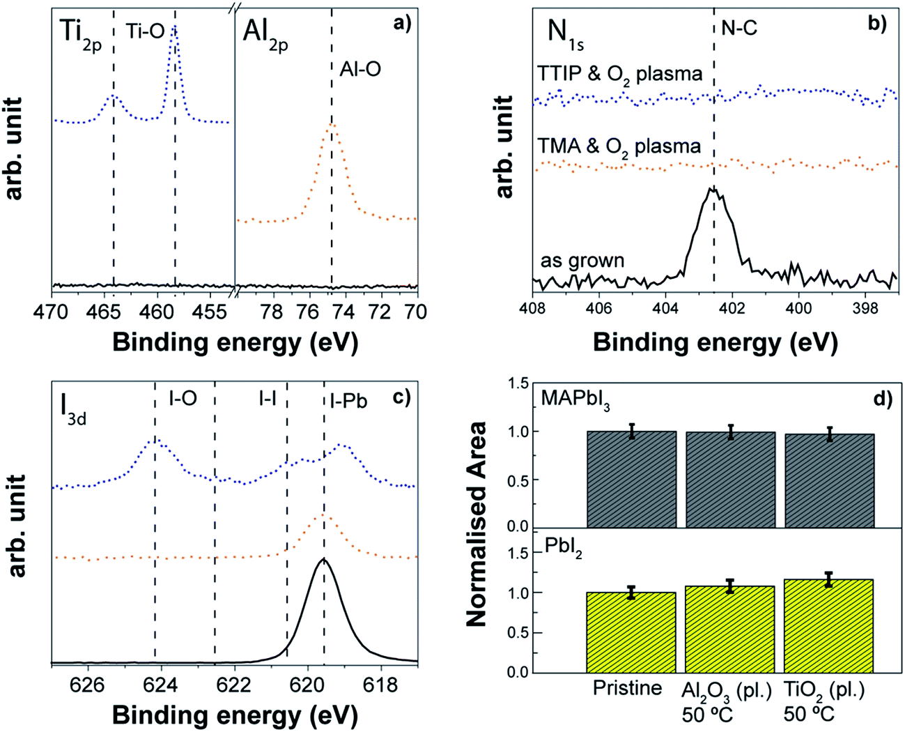 | ||
| Fig. 14 XPS analysis for three perovskite samples: pristine, upon plasma-assisted ALD Al2O3 and TiO2 process. (a) Al2p and Ti2p (b) N1s (c) I3d (d) normalized areas of the {110} peak of the perovskite, MAPbI3, and PbI2 {001} peak. | ||
4.4. Comparing plasma assisted ALD processes for TiO2, NiO and MoO3
Based on the results in the previous section, we selected low temperature plasma assisted processes for TiO2, NiO and MoO3 which can potentially be adopted as selective contacts in the various perovskite device architectures. First of all, the plasma assisted ALD process of TiO2 based on the common titanium isopropoxide (TTIP) precursor as the Ti source was compared with the one for Al2O3. The TiO2 process has been chosen since TiO2 is the typical ETL material, and it can be a valid candidate to be deposited on top of the perovskite absorber in the p–i–n architecture. The layers were deposited at 50 °C using the same working pressure, O2 flow and RF power to ignite the plasma, except that in the case of the TiO2 process the length of the O2 plasma step is longer, which is required to guarantee the ALD behavior of the metal oxide growth (see Table S2†) according to the earlier defined developed processes. The XPS analysis reveals that TiO2 can grow on top of the perovskite, as confirmed by the presence of the Ti peak at 458.6 eV (see Fig. 14a) related to the Ti–O bond. The nitrogen content is still affected (Fig. 14b), and the XRD analysis shows only a negligible variation in the perovskite crystallinity and in the formation of PbI2 (Fig. 14d), very similar to the one reported for the Al2O3. However, the XPS iodine spectrum (Fig. 14c) reveals the formation of iodate species (624 eV and 622.7 eV) and I2 (621 eV), in contrast to what we see for the Al2O3 case. This result might be explained by the longer O2 plasma exposure, as well as by the lower growth per cycle (GPC) of the TiO2 process (0.05 nm per cycle) with respect to the Al2O3 one (0.12 nm per cycle). Indeed, the initial TTIP precursor absorbed on the surface might provide a lower surface coverage with respect to the case with TMA, increasing the exposure of the perovskite structure to O2 plasma. Potentially, different titanium metal precursors, such as titanium tetrachloride (TiCl4) and tetrakis(dimethylamino)titanium (TDMAT) might be investigated to replace TTIP, due to their higher growth per cycle (>0.06 nm per cycle),212,216–218 with the target of reducing the change in the perovskite chemistry. Despite the fact that the perovskite crystallinity remains unaffected as confirmed by the XRD analysis after TiO2 growth, it needs to be seen whether the removal of nitrogen from the perovskite surface and the variation in the iodine content are significantly detrimental in device applications. Therefore, the adoption of water vapour as a co-reactant instead of O2 plasma might be favoured. Efficient low temperature thermal ALD processes have been reported in the literature with the TiCl4212 and TDMAT precursors,218 as well as the TTIP in the case of spatial ALD.182A similar behavior for the surface modification and the crystallinity of the MAPbI3 has been observed also when plasma assisted ALD processes of NiO and MoO3 (at 50 °C) were employed (see Fig. 15). Both materials can be deposited on top of the perovskite absorber as demonstrated by the presence of the corresponding peaks for metal oxides (Fig. 15a). The nitrogen still disappears in the case of the NiO process, while the N contribution from the perovskite after the MoO3 deposition cannot be precisely determined since the N1s signal overlaps with the most intense Mo3p peak. Additionally, nitrogen can originate also from the metal oxide layer deposition, due to the residues of the molybdenum precursor ligands that contain N–C bonds. The I3d spectrum for both the plasma assisted ALD films reveals the presence of iodate species (see Fig. 15c), indicating that the interaction between the perovskite surface and the O2 plasma still occurs irrespective of the different ALD metal precursors and plasma exposure lengths (see Table S2†). Regarding the MAPbI3 crystallinity, the MAPbI3 exhibits a more pronounced degradation in the main XRD perovskite peak after the MoO3 deposition, almost 30% in respect to the as-grown reference sample, whereas no visible variations are observed after the NiO process (Fig. 15d).
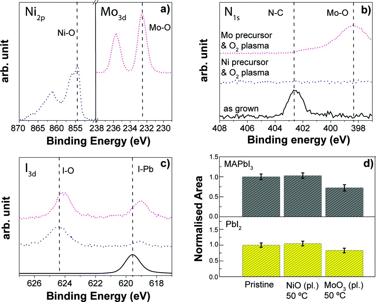 | ||
| Fig. 15 XPS analysis for three perovskite samples: pristine, upon the NiO plasma assisted ALD process (Ni(C5H4CH3)2 & O2 plasma) and the MoO3 plasma assisted ALD process (Mo(NtBu)2(NMe2)2 & O2 plasma). (a) Ni2p and Mo3d (b) N1s (c) I3d. (d) Comparison of the normalized area of the {110} peak of the perovskite MAPbI3, and the PbI2 {001} peak for the 3 samples. | ||
4.5. Comparing thermal ALD processes for Al2O3 and ZnO
Finally, we investigated the effect of a thermal ALD process of ZnO, and compared it to the baseline thermal process of Al2O3. The depositions were carried out in the same reactor with the same working conditions and the ALD parameters such as precursors and co-reactant dosing times, and purges were very similar (see Table S2†).As reported in Section 4.2, the deposition at 80 °C of 60 ALD cycles of Al2O3 (nominally 6 nm) enables the growth of the layer. Both the Al2p and the O1s peaks are discernible at 74.6 eV and 532 eV respectively (see Fig. 13a and Fig. 16b) and the XRD analysis reveals a minor change in the perovskite crystallinity (Fig. 16d). The same result, not reported here, has been observed when the deposition was carried out at 120 °C for the same amount of ALD cycles (the length of the process was 10 min). In contrast to the Al2O3 case, no growth is observed after 40 ALD cycles for ZnO (nominally 6 nm, length of the process less than 8 min), since neither the Zn2p peak (1022 eV) nor the O1s peak (at 530.5 eV) was detected by XPS, whereas the two peaks are clearly noticeable on the silicon reference sample placed inside the reactor together with the perovskite layer. In order to exclude the presence of a nucleation delay regime on top of the perovskite film, we also extended the number of the ALD cycles to 100, for a nominal thickness of 15 nm. The oxygen peak still remained absent, although a small peak (relative amount 2.5%) of zinc was discerned (see Fig. 16c). The chemical attribution of this peak remains unclear due to the complete absence of oxygen. Therefore, it appears that the diethylzinc (DEZ) precursor cannot effectively react to initiate the growth of ZnO on the perovskite surface for up to 100 cycles, different from what we observed in the case of TMA and H2O based processes. Furthermore, the nitrogen peak intensity reduces with the number of cycles which indicates that the degradation of the organic part of the perovskite material is also a function of precursor/co reactant exposures. Since the H2O exposure alone (for 50 times simulating the half ALD cycle) did not reduce the nitrogen peak as reported in Section 4.1 (see Fig. 12a), this effect can be attributed to the DEZ interaction with the MAPbI3. The effect of the perovskite degradation becomes evident in the XRD analysis (Fig. 16d). The ALD ZnO process (100 cycles) induces a significant loss of almost 80% of the main perovskite peak and the huge increase (up to 40 times) of the PbI2 peak. A similar effect was reported by Choudhury et al.,214 investigating the sequential dosages of TMA over the mixed halide perovskite (MAPbI3−xClx). In their work, they observed a continuous mass loss ascribed to the removal of the methylammonium with the main consequence of the complete disappearance of the perovskite peak from the XRD spectrum and the presence of only the PbI2 peak after 100 TMA pulses. In the literature, only Hoye et al.203 demonstrated the feasible direct deposition of ZnO (and also ZnxMg1−xO) over a pure bromide perovskite film (MAPbBr3) by means of spatial atmospheric ALD. It is plausible that both the different nature of the spatial ALD process (atmospheric pressure, 60 °C, 3 min) as well as the presence of bromine instead of iodine which is well known to give a more stable material, can explain the differences between their and our case. This result highlights that the compatibility of ALD for growth-on-perovskite applications is highly dependent on the specific ALD process, and even more importantly, on the specific interaction that the precursors have with the perovskite layer. Although the thermal ALD ZnO and Al2O3 processes are considered quite similar in the ALD community, the compatibility with the MAPbI3 is completely different. Whilst it does not exclude ZnO as a possibility in this case, it indicates that the development of the process needs the understanding of the DEZ/perovskite chemical interaction.
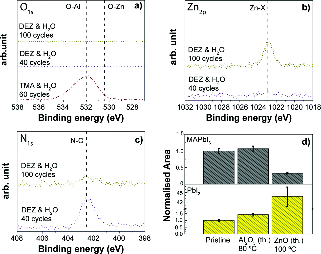 | ||
| Fig. 16 XPS analysis of three perovskite samples: pristine, upon thermal ALD Al2O3 and ZnO processes. (a) O1s (b) Zn2p (c) N1s (d) normalized areas of the {110} peak of the perovskite, MAPbI3, and PbI2 {001} peak. | ||
5. Conclusion and outlook
In order to make the perovskite PV technology mature, generating highly efficient devices with a long stability on a large area, the optimization of all the components is still required for single junction solar cells and also in the case of tandem configurations with silicon or CIGS devices. The adoption of atomic layer deposition processes has the potential to tackle these challenges, due to the indisputable benefits that this technique can offer in terms of thickness accuracy, high conformal layers and control of the opto-electrical properties of the deposited films over other deposition methods. Indeed, ALD is gaining momentum in the field of perovskite solar cells, following a trend very similar to what occurred for c-Si and thin film PV technologies where the ALD technique has been explored and in some cases, adopted over other deposition methods.The ALD layers that have been already successfully introduced in perovskite architectures have been initially reviewed, highlighting that their application mainly focused on two specific functional layers: (i) n-type ETL (TiO2, SnO2, ZnO) metal oxides, and (ii) passivation layers with ultra-thin (3–6 nm) TiO2 films or sub nanometer Al2O3 layers. Nonetheless, ALD processes have already been developed for a large variety of materials which have been deposited by means of other methods (solution processing, sputtering, or thermal evaporation) and therefore can be potentially explored and adopted in the various perovskite configurations: ALD p-type (NiO, Cu2O), high work function (MoO3), and wide band gap (Ga2O3, MgO, HfO2) metal oxides, TCOs (doped ZnO, In2O3:H) and also metals (platinum, silver).
So far, the majority of the investigated ALD layers was applied prior to the perovskite deposition in the various device configurations. In this case, metal oxide ALD processes have to be carried out on stable materials (glass, TCOs, metal oxide nanoparticles) which give researchers a great degree of choice in the deposition temperature range, the type of metal precursor and oxidant agent, and the processing parameters as we summarized in the various tables reported in the main text. Also in the case of depositions on polymer substrates (PET and PEN) coated by ITO films, where the maximum processing temperature is 150 °C, the plasma assisted approach (and potentially spatial ALD processes) can fulfill the processing conditions required by these temperature sensitive substrates.
A completely different scenario has to be faced by researchers when ALD layers have to be processed directly on top of the perovskite film. Since the organo-lead halides are soft materials, exhibiting poor stability when exposed to high temperatures, moisture, oxygen and UV light, a careful evaluation of the effect of the ALD working conditions and the type of metal precursor and oxidant agent on the chemical and crystal structure stability of the perovskite layer has to be made.
We observed that methylammonium lead iodide perovskite films were already degraded under prolonged (i.e. few hours) annealing at 100 °C under low vacuum conditions inside an ALD reactor chamber. Nevertheless, shorter thermal induced stress (1 h) at 100 °C pointed out that it is the total thermal budget (temperature and time) the main parameter which has to be optimized to avoid the material degradation. Next to the obvious efforts in increasing the thermal stability of the perovskite layer, the development of efficient ALD processes which require low thermal budget for the deposition of the appropriate metal oxides should be addressed. While speeding up the ALD process is one of the benefits of spatial ALD processes, the reduction of processing temperature can be easily achieved by the use of O2 plasma exposure in replacement of H2O as a co-reactant in the generation of metal oxides.
We demonstrated the validity of this approach by low temperature (50 °C) plasma assisted processes for Al2O3, TiO2, NiO and MoO3 layers, enabling the growth of the corresponding metal oxides on top of the MAPbI3, although chemical changes at the perovskite surface and slight changes in crystallinity are detectable. In particular, the O2 plasma step is found to be responsible for the removal of the methylammonium cation and the formation of iodate species, the effect of which on the device performance has to be carefully evaluated.
Alternative to the plasma assisted approach, the use of H2O as a co-reactant instead of O2 plasma is highly promising, although higher processing temperatures (80–100 °C) are required to have efficient ALD processes. The low partial pressure of water required in the ALD process is not detrimental for the perovskite layer used in this study, opening opportunities for the adoption of thermal ALD processes. Nonetheless, the comparison we proposed between the Al2O3 and the ZnO process highlights how the growth of the metal oxide can be significantly affected by the chemistry of the metal precursor. Therefore, the development of ad hoc ALD processes targeting ALD deposition over the organo-lead halide material needs to carefully consider several aspects.
The achievement of growing efficient metal oxides directly on top of the perovskite is extremely attractive, since it will give the opportunity to generate perovskite solar cells where both the ETLs and HTLs can be deposited by a single powerful technique, which provides high quality layers and has the potential to be upscaled for industrial mass production. Furthermore, the adoption of metal oxides for efficient ETLs and HTLs in replacement of organic selective materials (i.e. the case of PEDOT:PSS or Spiro-MeOTAD) has been already tested as a valid strategy to improve the stability of the devices, although adopting solution processed MOs. Therefore, an architecture where the perovskite absorber is sandwiched between two ALD metal oxides, such as the one depicted in Fig. 17, may become highly desired. In this view, after the process compatibility is provided, the quality of ALD layers as selective contacts remains to be explored.
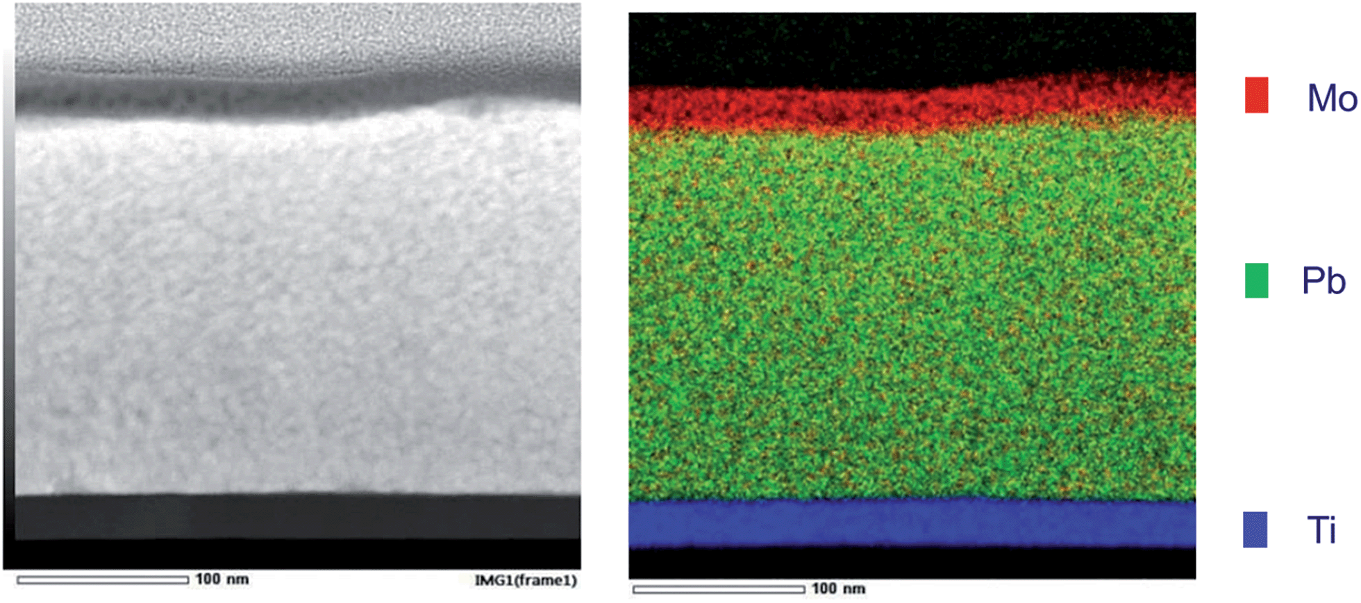 | ||
| Fig. 17 Proof of concept of a methylammonium lead iodide film sandwiched between two plasma assisted ALD layers: on the bottom 25 nm of TiO2 deposited at 150 °C and on top 20 nm of MoO3 deposited at 50 °C. Left: high-angle annular dark field scanning TEM image. Right: corresponding elemental mapping acquired using energy dispersive X-ray spectroscopy. | ||
Acknowledgements
We are grateful for financial support from the Dutch Ministry of Economic Affairs, via The Top-consortia Knowledge and Innovation (TKI) Program “High Efficiency Hybrid Tandem Solar Cells” (TEZ0214010). We acknowledge ENERGY.2012.10.2.1 (NANOMATCELL, grant agreement no. 308997). The research of M. C. has been funded by the Netherlands Organization for Scientific Research (NWO, Aspasia programma).References
- S. M. George, Chem. Rev., 2010, 110, 111–131 CrossRef CAS PubMed.
- M. Leskelä and M. Ritala, Thin Solid Films, 2002, 409, 138–146 CrossRef.
- H. B. Profijt, S. E. Potts, M. C. M. van de Sanden and W. M. M. Kessels, J. Vac. Sci. Technol., A, 2011, 29, 50801 Search PubMed.
- D. Garcia-Alonso, S. E. Potts, C. A. A. van Helvoirt, M. A. Verheijen and W. M. M. Kessels, J. Mater. Chem. C, 2015, 3, 3095–3107 RSC.
- Y. Wu, P. M. Hermkens, B. W. H. van de Loo, H. C. M. Knoops, S. E. Potts, M. A. Verheijen, F. Roozeboom and W. M. M. Kessels, J. Appl. Phys., 2013, 114, 24308 CrossRef.
- H. C. M. Knoops, L. Baggetto, E. Langereis, M. C. M. van de Sanden, J. H. Klootwijk, F. Roozeboom, R. A. H. Niessen, P. H. L. Notten and W. M. M. Kessels, ECS Trans., 2007, 11, 45–54 CAS.
- X. Meng, X.-Q. Yang and X. Sun, Adv. Mater., 2012, 24, 3589–3615 CrossRef CAS PubMed.
- H. C. M. Knoops, M. E. Donders, M. C. M. van de Sanden, P. H. L. Notten and W. M. M. Kessels, J. Vac. Sci. Technol. A, 2012, 30, 10801 Search PubMed.
- M. J. Weber, A. J. M. Mackus, M. A. Verheijen, C. van der Marel and W. M. M. Kessels, Chem. Mater., 2012, 24, 2973–2977 CrossRef CAS.
- S. T. Christensen, H. Feng, J. L. Libera, N. Guo, J. T. Miller, P. C. Stair and J. W. Elam, Nano Lett., 2010, 10, 3047–3051 CrossRef CAS PubMed.
- N. P. Dasgupta, C. Liu, S. Andrews, F. B. Prinz and P. Yang, J. Am. Chem. Soc., 2013, 135, 12932–12935 CrossRef CAS PubMed.
- E. Langereis, M. Creatore, S. B. S. Heil, M. C. M. van de Sanden and W. M. M. Kessels, Appl. Phys. Lett., 2006, 89, 81915 CrossRef.
- W. Keuning, P. van de Weijer, H. Lifka, W. M. M. Kessels and M. Creatore, J. Vac. Sci. Technol., A, 2012, 30, 01A131 Search PubMed.
- G. K. Hyde, S. D. McCullen, S. Jeon, S. M. Stewart, H. Jeon, E. G. Loboa and G. N. Parsons, Biomed. Mater., 2009, 4, 25001 CrossRef CAS PubMed.
- J. A. van Delft, D. Garcia-Alonso and W. M. M. Kessels, Semicond. Sci. Technol., 2012, 27, 74002 CrossRef.
- J. R. Bakke, K. L. Pickrahn, T. P. Brennan and S. F. Bent, Nanoscale, 2011, 3, 3482–3508 RSC.
- X. Li, D. Bi, C. Yi, J.-D. Décoppet, J. Luo, S. M. Zakeeruddin, A. Hagfeldt and M. Grätzel, Science, 2016, 131, 6050–6051 Search PubMed.
- S. Kazim, M. K. Nazeeruddin, M. Grätzel and S. Ahmad, Angew. Chem., Int. Ed., 2014, 53, 2812–2824 CrossRef CAS PubMed.
- H. J. Snaith, J. Phys. Chem. Lett., 2013, 4, 3623–3630 CrossRef CAS.
- K. Deng and L. Li, Adv. Mater. Interfaces, 2016, 3, 1600505 CrossRef.
- M. A. Green, A. Ho-Baillie and H. J. Snaith, Nat. Photonics, 2014, 8, 506–514 CrossRef CAS.
- M. Grätzel, Nat. Mater., 2014, 13, 838–842 CrossRef PubMed.
- A. Kojima, K. Teshima, Y. Shirai and T. Miyasaka, J. Am. Chem. Soc., 2009, 131, 6050–6051 CrossRef CAS PubMed.
- H.-S. Kim, C.-R. Lee, J.-H. Im, K.-B. Lee, T. Moehl, A. Marchioro, S.-J. Moon, R. Humphry-Baker, J.-H. Yum, J. E. Moser, M. Grätzel and N.-G. Park, Sci. Rep., 2012, 2, 591 Search PubMed.
- S. De Wolf, J. Holovsky, S. J. Moon, P. Loper, B. Niesen, M. Ledinsky, F. J. Haug, J. H. Yum and C. Ballif, J. Phys. Chem. Lett., 2014, 5, 1035–1039 CrossRef CAS PubMed.
- S. D. Stranks, G. E. Eperon, G. Grancini, C. Menelaou, M. J. P. Alcocer, T. Leijtens, L. M. Herz, A. Petrozza and H. J. Snaith, Science, 2013, 342, 341–344 CrossRef CAS PubMed.
- Q. Lin, A. Armin, R. C. R. Nagiri, P. L. Burn and P. Meredith, Nat. Photonics, 2014, 9, 106–112 CrossRef.
- A. Miyata, A. Mitioglu, P. Plochocka, O. Portugall, J. T.-W. Wang, S. D. Stranks, H. J. Snaith and R. J. Nicholas, Nat. Phys., 2015, 11, 582–587 CrossRef CAS.
- Y.-C. Hsiao, T. Wu, M. Li, Q. Liu, W. Qin and B. Hu, J. Mater. Chem. A, 2015, 3, 15372–15385 CAS.
- L. Yang, A. T. Barrows, D. G. Lidzey and T. Wang, Rep. Prog. Phys., 2016, 79, 26501 CrossRef PubMed.
- J. Burschka, N. Pellet, S.-J. Moon, R. Humphry-Baker, P. Gao, M. K. Nazeeruddin and M. Grätzel, Nature, 2013, 499, 316–319 CrossRef CAS PubMed.
- M. M. Lee, J. Teuscher, T. Miyasaka, T. N. Murakami and H. J. Snaith, Science, 2012, 338, 643–647 CrossRef CAS PubMed.
- S. H. Hwang, J. Roh, J. Lee, J. Ryu, J. Yun and J. Jang, J. Mater. Chem. A, 2014, 2, 16429–16433 CAS.
- V. Trifiletti, V. Roiati, S. Colella, R. Giannuzzi, L. De Marco, A. Rizzo, M. Manca, A. Listorti and G. Gigli, ACS Appl. Mater. Interfaces, 2015, 7, 4283–4289 CAS.
- P. Gao, M. Grätzel and M. K. Nazeeruddin, Energy Environ. Sci., 2014, 7, 2448 CAS.
- A. Mei, X. Li, L. Liu, Z. Ku, T. Liu, Y. Rong, M. Xu, M. Hu, J. Chen, Y. Yang, M. Grätzel and H. Han, Science, 2014, 345, 295–298 CrossRef CAS PubMed.
- W. A. Laban and L. Etgar, Energy Environ. Sci., 2013, 6, 3249–3253 CAS.
- M. Liu, M. B. Johnston and H. J. Snaith, Nature, 2013, 501, 395–398 CrossRef CAS PubMed.
- J.-H. Heo, H. J. Han, D. Kim, T. Ahn and S. H. Im, Energy Environ. Sci., 2015, 8, 1602–1608 CAS.
- C. Momblona, L. Gil-Escrig, E. Bandiello, E. M. Hutter, M. Sessolo, K. Lederer, J. Blochwitz-Nimoth and H. J. Bolink, Energy Environ. Sci., 2016, 9, 3456–3463 CAS.
- L. Serrano-Lujan, N. Espinosa, T. T. Larsen-Olsen, J. Abad, A. Urbina and F. C. Krebs, Adv. Energy Mater., 2015, 5, 1501119 CrossRef.
- N. Espinosa, L. Serrano-Luján, A. Urbina and F. C. Krebs, Sol. Energy Mater. Sol. Cells, 2015, 137, 303–310 CrossRef CAS.
- G. Richardson, S. O'Kane, R. G. Niemann, T. Peltola, J. M. Foster, P. J. Cameron and A. Walker, Energy Environ. Sci., 2016, 9, 1476–1485 CAS.
- Y. Zhang, M. Liu, G. E. Eperon, T. C. Leijtens, D. McMeekin, M. Saliba, W. Zhang, M. de Bastiani, A. Petrozza, L. M. Herz, M. B. Johnston, H. Lin and H. J. Snaith, Mater. Horiz., 2015, 1, 96 Search PubMed.
- S. Meloni, T. Moehl, W. Tress, M. Franckevičius, M. Saliba, Y. H. Lee, P. Gao, M. K. Nazeeruddin, S. M. Zakeeruddin, U. Rothlisberger and M. Graetzel, Nat. Commun., 2016, 7, 10334 CrossRef CAS PubMed.
- C. Li, S. Tscheuschner, F. Paulus, P. E. Hopkinson, J. Kießling, A. Köhler, Y. Vaynzof and S. Huettner, Adv. Mater., 2016, 8, 2446–2454 CrossRef PubMed.
- J. Seo, J. H. Noh and S. I. Seok, Acc. Chem. Res., 2016, 49, 562–572 CrossRef CAS PubMed.
- P. Schulz, E. Edri, S. Kirmayer, G. Hodes, D. Cahen and A. Kahn, Energy Environ. Sci., 2014, 7, 1377–1381 CAS.
- F. Wang, Z. Tan and Y. Li, Energy Environ. Sci., 2015, 8, 1059–1091 CAS.
- J. Kim, H. Lee, H. P. Kim, T. Lin, A. Kanwat, A. Rashid bin Mohd Yusoff and J. Jang, Nanoscale, 2016, 8, 9284–9292 RSC.
- L. Hu, J. Peng, W. Wang, Z. Xia, J. Yuan and J. Lu, ACS Photonics, 2014, 1, 547–553 CrossRef CAS.
- S. Chatterjee and A. J. Pal, J. Phys. Chem. C, 2016, 120, 1428–1437 CAS.
- Z. Wu, S. Bai, J. Xiang, Z. Yuan, Y. Yang, W. Cui, X. Gao, Z. Liu, Y. Jin and B. Sun, Nanoscale, 2014, 6, 10505–10510 RSC.
- A. K. K. Kyaw, X. W. Sun, C. Y. Jiang, G. Q. Lo, D. W. Zhao and D. L. Kwong, Appl. Phys. Lett., 2008, 93, 221107, DOI:10.1063/1.3039076.
- C. Battaglia, X. Yin, M. Zheng, I. D. Sharp, T. Chen, S. McDonnell, A. Azcatl, C. Carraro, B. Ma, R. Maboudian, R. M. Wallace and A. Javey, Nano Lett., 2014, 14, 967–971 CrossRef CAS PubMed.
- X. Hu, L. Chen and Y. Chen, J. Phys. Chem. C, 2014, 118, 9930–9938 CAS.
- Y.-C. Tseng, A. U. Mane, J. W. Elam and S. B. Darling, Sol. Energy Mater. Sol. Cells, 2012, 99, 235–239 CrossRef CAS.
- J. H. Noh, N. J. Jeon, Y. C. Choi, M. K. Nazeeruddin, M. Grätzel and S. Il Seok, J. Mater. Chem. A, 2013, 1, 11842 CAS.
- J. Seo, S. Park, Y. Chan Kim, N. J. Jeon, J. H. Noh, S. C. Yoon, S. Il Seok and P. S. Cells, Energy Environ. Sci., 2014, 7, 2642 CAS.
- W. Chen, Y. Wu, Y. Yue, J. Liu, W. Zhang, X. Yang, H. Chen, E. Bi, I. Ashraful, M. Grätzel and L. Han, Science, 2015, 350, 944–948 CrossRef CAS PubMed.
- D. Liu and T. L. Kelly, Nat. Photonics, 2013, 8, 133–138 CrossRef.
- M.-H. Yeh, S.-J. Ho, K.-C. Wang, H.-R. Hsu, G.-H. Chen and H.-S. Chen, Sol. Energy, 2016, 129, 116–125 CrossRef CAS.
- S. Merdes, A. Steigert, F. Ziem, I. Lauermann, R. Klenk, F. Hergert, C. A. Kaufmann and R. Schlatmann, Thin Solid Films, 2015, 574, 28–31 CrossRef CAS.
- T. Prem, M. J. Kim, H. Jeong, S. Hwang, N. L. Tarwal and Y. K. Jeong, 39th IEEE Photovolt. Spec. Conf., 2013, 1992–1995, DOI:10.1109/PVSC.2013.6744862.
- Y. Wu, X. Yang, H. Chen, K. Zhang, C. Qin, J. Liu, W. Peng, A. Islam, E. Bi, F. Ye, M. Yin, P. Zhang and L. Han, Appl. Phys. Express, 2014, 7, 52301 CrossRef.
- F. Di Giacomo, V. Zardetto, G. Lucarelli, L. Cinà, A. Di Carlo, M. Creatore and T. M. Brown, Nano Energy, 2016, 30, 460–469 CrossRef CAS.
- V. Zardetto, F. Di Giacomo, G. Lucarelli, W. M. M. Kessels, T. M. Brown and M. Creatore, 2016, submitted.
- F. Di Giacomo, V. Zardetto, A. D'Epifanio, S. Pescetelli, F. Matteocci, S. Razza, A. Di Carlo, S. Licoccia, W. M. M. Kessels, M. Creatore and T. M. Brown, Adv. Energy Mater., 2015, 5, 1401808, DOI:10.1002/aenm.201401808.
- B.-J. Kim, D. H. Kim, Y.-Y. Lee, H.-W. Shin, G. S. Han, J. S. Hong, K. Mahmood, T. Ahn, Y.-C. Joo, K. S. Hong, N.-G. Park, S. Lee and H. S. Jung, Energy Environ. Sci., 2015, 8, 916–921 CAS.
- J. P. Correa Baena, L. Steier, W. Tress, M. Saliba, S. Neutzner, T. Matsui, F. Giordano, T. J. Jacobsson, A. R. Srimath Kandada, S. M. Zakeeruddin, A. Petrozza, A. Abate, M. K. Nazeeruddin, M. Grätzel and A. Hagfeldt, Energy Environ. Sci., 2015, 8, 2928–2934 CAS.
- J. P. Mailoa, C. D. Bailie, E. C. Johlin, E. T. Hoke, A. J. Akey, W. H. Nguyen, M. D. McGehee and T. Buonassisi, Appl. Phys. Lett., 2015, 106, 10–14 CrossRef.
- S. Albrecht, M. Saliba, J. P. Correa Baena, F. Lang, L. Kegelmann, M. Mews, L. Steier, A. Abate, J. Rappich, L. Korte, R. Schlatmann, M. K. Nazeeruddin, A. Hagfeldt, M. Grätzel and B. Rech, Energy Environ. Sci., 2016, 9, 81–88 CAS.
- C. Wang, D. Zhao, C. Grice, W. Liao, Y. Yu, A. Cimaroli, N. Shrestha, P. J. Roland, J. Chen, Z. Yu, P. Liu, N. Cheng, R. Ellingson, X. Zhao and Y. Yan, J. Mater. Chem. A, 2016, 4, 12080–12087 CAS.
- X. Dong, H. Hu, B. Lin, J. Ding and N. Yuan, Chem. Commun., 2014, 50, 14405–14408 RSC.
- C. Y. Chang, K. T. Lee, W. K. Huang, H. Y. Siao and Y. C. Chang, Chem. Mater., 2015, 27, 5122–5130 CrossRef CAS.
- A. K. Chandiran, M. Abdi-Jalebi, A. Yella, M. I. Dar, C. Yi, S. A. Shivashankar, M. K. Nazeeruddin and M. Grätzel, Nano Lett., 2014, 14, 1190–1195 CrossRef CAS PubMed.
- T. Leijtens, S. D. Stranks, G. E. Eperon, R. Lindblad, E. M. J. Johansson, J. M. Ball, M. M. Lee, H. J. Snaith and I. J. Mcpherson, ACS Nano, 2014, 8, 7147–7155 CrossRef CAS PubMed.
- J. You, L. Meng, T.-B. Song, T.-F. Guo, Y. Yang, W.-H. Chang, Z. Hong, H. Chen, H. Zhou, Q. Chen, Y. Liu, N. De Marco and Y. Yang, Nat. Nanotechnol., 2016, 11, 75–81 CrossRef CAS PubMed.
- H. Zhang, J. Cheng, F. Lin, H. He, J. Mao, K. S. Wong, A. K.-Y. Jen and W. C. H. Choy, ACS Nano, 2016, 10, 1503–1511 CrossRef CAS PubMed.
- J. Y. Jeng, K. C. Chen, T. Y. Chiang, P. Y. Lin, T. Da Tsai, Y. C. Chang, T. F. Guo, P. Chen, T. C. Wen and Y. J. Hsu, Adv. Mater., 2014, 26, 4107–4113 CrossRef CAS PubMed.
- V. Trifiletti, V. Roiati, S. Colella, R. Giannuzzi, L. De Marco, A. Rizzo, M. Manca, A. Listorti and G. Gigli, ACS Appl. Mater. Interfaces, 2015, 7, 4283–4289 CAS.
- K. X. Steirer, P. F. Ndione, N. E. Widjonarko, M. T. Lloyd, J. Meyer, E. L. Ratcliff, A. Kahn, N. R. Armstrong, C. J. Curtis, D. S. Ginley, J. J. Berry and D. C. Olson, Adv. Energy Mater., 2011, 1, 813–820 CrossRef CAS.
- S. Seo, I. J. Park, M. Kim, S. Lee, C. Bae, H. S. Jung, N.-G. Park, J. Y. Kim and H. Shin, Nanoscale, 2016, 8, 11403–11412 RSC.
- T. S. Yang, W. Cho, M. Kim, K.-S. An, T.-M. Chung, C. G. Kim and Y. Kim, J. Vac. Sci. Technol., A, 2005, 23, 1238 CAS.
- H. L. Lu, G. Scarel, X. L. Li and M. Fanciulli, J. Cryst. Growth, 2008, 310, 5464–5468 CrossRef CAS.
- S. J. Song, S. W. Lee, G. H. Kim, J. Y. Seok, K. J. Yoon, J. H. Yoon, C. S. Hwang, J. Gatineau and C. Ko, Chem. Mater., 2012, 24, 4675–4685 CrossRef CAS.
- Y.-H. You, B.-S. So, J.-H. Hwang, W. Cho, S. S. Lee, T.-M. Chung, C. G. Kim and K.-S. An, Appl. Phys. Lett., 2006, 89, 222105 CrossRef.
- E. Thimsen, A. B. F. Martinson, W. Elam and M. J. Pellin, J. Phys. Chem. C, 2012, 116, 16830–16840 CAS.
- H. Kumagai, M. Matsumoto, K. Toyoda and M. Obara, J. Mater. Sci. Lett., 1996, 15, 1081–1083 CrossRef CAS.
- J. W. Shim, C. Fuentes-Hernandez, A. Dindar, Y. Zhou, T. M. Khan and B. Kippelen, Org. Electron., 2013, 14, 2802–2808 CrossRef CAS.
- W. Yu, F. Li, H. Wang, E. Alarousu, Y. Chen, B. Lin, L. Wang, M. N. Hedhili, Y. Li, K. Wu, X. Wang, O. F. Mohammed and T. T. Wu, Nanoscale, 2016, 8, 6173–6179 RSC.
- W. Sun, Y. Li, S. Ye, H. Rao, W. Yan, H. Peng, Y. Li, Z. Liu, S. Wang, Z. Chen, L. Xiao, Z. Bian and C. Huang, Nanoscale, 2016, 10806–10813 RSC.
- C. Zuo and L. Ding, Small, 2015, 11, 5528–5532 CrossRef CAS PubMed.
- H. Rao, S. Ye, W. Sun, W. Yan, Y. Li, H. Peng, Z. Liu, Z. Bian, Y. Li and C. Huang, Nano Energy, 2016, 27, 51–57 CrossRef CAS.
- S. W. Lee, Y. S. Lee, J. Heo, S. C. Siah, D. Chua, R. E. Brandt, S. B. Kim, J. P. Mailoa, T. Buonassisi and R. G. Gordon, Adv. Energy Mater., 2014, 4, 1–7 Search PubMed.
- H. Kim, M. Y. Lee, S. H. Kim, S. I. Bae, K. Y. Ko, H. Kim, K. W. Kwon, J. H. Hwang and D. J. Lee, Appl. Surf. Sci., 2015, 349, 673–682 CrossRef CAS.
- D. Munoz-Rojas, M. Jordan, C. Yeoh, A. T. Marin, A. Kursumovic, L. A. Dunlop, D. C. Iza, A. Chen, H. Wang and J. L. MacManus Driscoll, AIP Adv., 2012, 2, 42179 CrossRef.
- J.-D. Kwon, S.-H. Kwon, T.-H. Jung, K.-S. Nam, K.-B. Chung, D.-H. Kim and J.-S. Park, Appl. Surf. Sci., 2013, 285, 373–379 CrossRef CAS.
- T. Waechtler, S. Oswald, N. Roth, A. Jakob, H. Lang, R. Ecke, S. E. Schulz, T. Gessner, A. Moskvinova, S. Schulze and M. Hietschold, J. Electrochem. Soc., 2009, 156, H453 CrossRef CAS.
- Z. Li, A. Rahtu and R. G. Gordon, J. Electrochem. Soc., 2006, 153, C787 CrossRef CAS.
- H. Zhou, Q. Chen, G. Li, S. Luo, T. B. Song, H.-S. Duan, Z. Hong, J. You, Y. Liu and Y. Yang, Science, 2014, 345, 542–546 CrossRef CAS PubMed.
- B.-X. Chen, H.-S. Rao, W.-G. Li, Y.-F. Xu, H.-Y. Chen, D.-B. Kuang and C. Su, J. Mater. Chem. A, 2016, 4, 5647–5653 CAS.
- W. Chen, Y. Wu, Y. Yue, J. Liu, W. Zhang, X. Yang, H. Chen, E. Bi, I. Ashraful, M. Gratzel and L. Han, Science, 2015, 350, 944–948 CrossRef CAS PubMed.
- J. Wang, M. Qin, H. Tao, W. Ke, Z. Chen, J. Wan, P. Qin, L. Xiong, H. Lei, H. Yu and G. Fang, Appl. Phys. Lett., 2015, 106, 121104 CrossRef.
- J. H. Kim, P.-W. Liang, S. T. Williams, N. Cho, C.-C. Chueh, M. S. Glaz, D. S. Ginger and A. K.-Y. Jen, Adv. Mater., 2015, 27, 695–701 CrossRef CAS PubMed.
- J.-P. Niemelä, H. Yamauchi and M. Karppinen, Thin Solid Films, 2014, 551, 19–22 CrossRef.
- N. P. Dasgupta, S. Neubert, W. Lee, O. Trejo, J.-R. Lee and F. B. Prinz, Chem. Mater., 2010, 22, 4769–4775 CrossRef CAS.
- E. H. A. Granneman, V. I. Kuneznetsov and P. Vermont, ECS Trans., 2014, 61, 3–16 CrossRef CAS.
- G. Dingemans and W. M. M. Kessels, J. Vac. Sci. Technol. A, 2012, 30, 1–27 Search PubMed.
- M. A. Green, A. Wang and S. R. Wenham, IEEE Trans. Electron Devices, 1999, 46, 1940–1947 CrossRef CAS.
- A. K. Chandiran, N. Tetreault, R. Humphry-Baker, F. Kessler, E. Baranoff, C. Yi, M. K. Nazeeruddin and M. Grätzel, Nano Lett., 2012, 12, 3941–3947 CrossRef CAS PubMed.
- E. Barea, X. Xu, V. González-Pedro, T. Ripollés-Sanchis, F. Fabregat-Santiago and J. Bisquert, Energy Environ. Sci., 2011, 4, 3414 CAS.
- M. Shanmugam, B. Bills and M. F. Baroughi, 35th IEEE Photovolt. Spec. Conf., 2010, 003248–003252 Search PubMed.
- M. Shanmugam, M. F. Baroughi and D. Galipeau, Thin Solid Films, 2010, 518, 2678–2682 CrossRef CAS.
- E. Palomares, J. N. Clifford, S. A. Haque, T. Lutz and J. R. Durrant, J. Am. Chem. Soc., 2003, 125, 475–482 CrossRef CAS PubMed.
- S. Wu, H. Han, Q. Tai, J. Zhang, S. Xu, C. Zhou, Y. Yang, H. Hu, B. Chen, B. Sebo and X.-Z. Zhao, Nanotechnology, 2008, 19, 215704 CrossRef PubMed.
- T.-C. Tien, F.-M. Pan, L.-P. Wang, C.-H. Lee, Y.-L. Tung, S.-Y. Tsai, C. Lin, F.-Y. Tsai and S.-J. Chen, Nanotechnology, 2009, 20, 305201 CrossRef PubMed.
- A. K. Chandiran, A. Yella, M. T. Mayer, P. Gao, M. K. Nazeeruddin and M. Grätzel, Adv. Mater., 2014, 26, 4309–4312 CrossRef CAS PubMed.
- S. S. Mali, C. S. Shim, H. K. Park, J. Heo, P. S. Patil and C. K. Hong, Chem. Mater., 2015, 27, 1541–1551 CrossRef CAS.
- V. Zardetto, F. Di Giacomo, M. A. Mohammed, G. Lucarelli, S. Razza, A. D'Epifanio, S. Licoccia, W. M. M. Kessels, A. Di Carlo, T. M. Brown and M. Creatore, ECS Trans., 2015, 69, 15–22 CrossRef.
- V. Zardetto, M. A. Mohammed, F. Di Giacomo, M. A. Verheijen, I. Sanchez Molina, S. A. Haque, A. Di Carlo, W. M. M. Kessels and M. Creatore, unpublished work.
- Y. H. Lee, J. Luo, M.-K. Son, P. Gao, K. T. Cho, J. Seo, S. M. Zakeeruddin, M. Grätzel and M. K. Nazeeruddin, Adv. Mater., 2016, 28, 3966–3972 CrossRef CAS PubMed.
- Y. Ogomi, K. Kukihara, S. Qing, T. Toyoda, K. Yoshino, S. Pandey, H. Momose and S. Hayase, ChemPhysChem, 2014, 15, 1062–1069 CrossRef CAS PubMed.
- G. S. Han, H. S. Chung, B. J. Kim, D. H. Kim, J. W. Lee, B. S. Swain, K. Mahmood, J. S. Yoo, N.-G. Park, J. H. Lee and H. S. Jung, J. Mater. Chem. A, 2015, 3, 9160–9164 CAS.
- H. Wei, J. Shi, X. Xu, J. Xiao, J. Luo, J. Dong, S. Lv, L. Zhu, H. Wu, D. Li, Y. Luo, Q. Meng and Q. Chen, Phys. Chem. Chem. Phys., 2015, 17, 4937–4944 RSC.
- Y. Shao, Z. Xiao, C. Bi, Y. Yuan and J. Huang, Nat. Commun., 2014, 5, 1–7 Search PubMed.
- J. Werner, S.-J. Moon, P. Löper, A. Walter, M. Filipi, C.-H. DWEng, L. Löfgren, J. Bailat, M. Topi, M. Morales-Masis, R. Peibst, R. Brendel, S. Nicolay, S. De Wolf, B. Niesen and C. Ballif, 31st EU PVSEC Proc., 2015, 66–71 Search PubMed.
- F. Fu, T. Feurer, T. Jäger, E. Avancini, B. Bissig, S. Yoon, S. Buecheler and A. N. Tiwari, Nat. Commun., 2015, 6, 8932 CrossRef CAS PubMed.
- T. P. White, N. N. Lal and K. R. Catchpole, J. Photovolt., 2014, 4, 208–214 CrossRef.
- P. Löper, S.-J. Moon, S. Martín de Nicolas, B. Niesen, M. Ledinsky, S. Nicolay, J. Bailat, J.-H. Yum, S. De Wolf and C. Ballif, Phys. Chem. Chem. Phys., 2015, 17, 1619–1629 RSC.
- D. P. McMeekin, G. Sadoughi, W. Rehman, G. E. Eperon, M. Saliba, M. T. Horantner, A. Haghighirad, N. Sakai, L. Korte, B. Rech, M. B. Johnston, L. M. Herz and H. J. Snaith, Science, 2016, 351, 151–155 CrossRef CAS PubMed.
- C. D. Bailie, J. P. Mailoa, E. C. Johlin, W. H. Nguyen, E. T. Hoke, A. J. Akey, T. Buonassisi and M. D. McGehee, in 2015 IEEE 42nd Photovoltaic Specialist Conference (PVSC), IEEE, 2015, pp. 1–3 Search PubMed.
- L. Kerkache, A. Layadi, F. Hadjersi, E. Dogheche, A. Gokarna, A. Stolz, M. Halbwax and J. P. Vilcot, Int. Conf. Renew. Energies Power Qual., 2010, 4–6 Search PubMed.
- X. Li, J. Pankow, B. To and T. Gessert, 33rd IEEE Photovolt. Spec. Conf. Photovoltage, 2008 DOI:10.1109/PVSC.2008.4922891.
- J. Werner, C. H. Weng, A. Walter, L. Fesquet, J. P. Seif, S. De Wolf, B. Niesen and C. Ballif, J. Phys. Chem. Lett., 2016, 7, 161–166 CrossRef CAS PubMed.
- L. Kranz, A. Abate, T. Feurer, F. Fu, E. Avancini, J. Löckinger, P. Reinhard, S. M. Zakeeruddin, M. Grätzel, S. Buecheler and A. N. Tiwari, J. Phys. Chem. Lett., 2015, 6, 2676–2681 CrossRef CAS PubMed.
- B. Macco, Y. Wu, D. Vanhemel and W. M. M. Kessels, Phys. Status Solidi RRL, 2014, 8, 987–990 CrossRef CAS.
- B. Macco, H. C. M. Knoops and W. M. M. Kessels, ACS Appl. Mater. Interfaces, 2015, 7, 16723–16729 CAS.
- J. Werner, G. Dubuis, A. Walter, P. Löper, S. J. Moon, S. Nicolay, M. Morales-Masis, S. De Wolf, B. Niesen and C. Ballif, Sol. Energy Mater. Sol. Cells, 2015, 141, 407–413 CrossRef CAS.
- K. A. Bush, C. D. Bailie, Y. Chen, A. R. Bowring, W. Wang, W. Ma, T. Leijtens, F. Moghadam and M. D. McGehee, Adv. Mater., 2016, 28, 3937–3943 CrossRef CAS PubMed.
- J. Werner, J. Geissbuehler, A. Dabirian, S. Nicolay, M. Morales Masis, S. De Wolf, B. Niesen and C. Ballif, ACS Appl. Mater. Interfaces, 2016, 8, 17260–17267 CAS.
- B. Macco, D. Deligiannis, S. Smit, R. A. C. M. M. van Swaaij, M. Zeman and W. M. M. Kessels, Semicond. Sci. Technol., 2014, 29, 122001 CrossRef.
- J. P. Mailoa, C. D. Bailie, E. C. Johlin, E. T. Hoke, A. J. Akey, W. H. Nguyen, M. D. McGehee and T. Buonassisi, Appl. Phys. Lett., 2015, 106, 10–14 CrossRef.
- B. Macco, M. F. J. Vos, N. F. W. Thissen, A. A. Bol and W. M. M. Kessels, Phys. Status Solidi RRL, 2015, 9, 393–396 CrossRef CAS.
- T. Todorov, T. Gershon, O. Gunawan, Y. S. Lee, C. Sturdevant, L. Y. Chang and S. Guha, Adv. Energy Mater., 2015, 5, 1–6 Search PubMed.
- T. Torndahl, C. Platzer-Bjorkman, J. Kessler and M. Edoff, Prog. Photovoltaics, 2007, 15, 225–235 Search PubMed.
- C. Platzer-Björkman, T. Törndahl, D. Abou-Ras, J. Malmström, J. Kessler and L. Stolt, J. Appl. Phys., 2006, 100, 44506 CrossRef.
- T. T. J. Lindahl, J. T. Watjen, A. Hultqvist, T. Ericson and M. Edoff, Prog. Photovoltaics, 2013, 21, 1588–1597 Search PubMed.
- A. Illiberi, C. Frijters, E. Balder, P. Poodt and F. Roozeboom, ECS Trans., 2015, 69, 31–37 CrossRef.
- P. R. Chalker, P. A. Marshall, S. Romani, J. W. Roberts, S. J. C. Irvine, D. A. Lamb, A. J. Clayton and P. A. Williams, J. Vac. Sci. Technol. A, 2013, 31, 01A120 Search PubMed.
- K. Saito, Y. Hiratsuka, A. Omata, H. Makino, S. Kishimoto, T. Yamamoto, N. Horiuchi and H. Hirayama, Superlattices Microstruct., 2007, 42, 172–175 CrossRef CAS.
- J. Werner, L. Barraud, A. Walter, M. Bräuninger, F. Sahli, D. Sacchetto, N. Tétreault, B. Paviet-Salomon, S.-J. Moon, C. Allebé, M. Despeisse, S. Nicolay, S. De Wolf, B. Niesen and C. Ballif, ACS Energy Lett., 2016, 1, 474–480 CrossRef CAS.
- M. Otto, M. Kroll, T. Käsebier, R. Salzer and R. B. Wehrspohn, Energy Procedia, 2012, 27, 361–364 CrossRef CAS.
- B. W. H. van de Loo, B. Macco, J. Melskens, M. A. Verheijen and W. M. M. Kessels, Photovoltaic Specialists Conference (PVSC), 2016 IEEE 43rd, DOI:10.1109/PVSC.2016.7750356.
- P. Loper, B. Niesen, S. J. Moon, S. Martin De Nicolas, J. Holovsky, Z. Remes, M. Ledinsky, F. J. Haug, J. H. Yum, S. De Wolf and C. Ballif, J. Photovolt., 2014, 4, 1545–1551 CrossRef.
- X. Zhang, Q. Huang, J. Hu, R. J. Knize and Y. Lu, Opt. Express, 2014, 22, A1400–A1411 CrossRef PubMed.
- A. J. M. MacKus, D. Garcia-Alonso, H. C. M. Knoops, A. A. Bol and W. M. M. Kessels, Chem. Mater., 2013, 25, 1769–1774 CrossRef CAS.
- Y. M. Yang, Q. Chen, Y.-T. Hsieh, T.-B. Song, N. De Marco, H. Zhou and Y. Yang, ACS Nano, 2015, 9, 7714–7721 CrossRef CAS PubMed.
- T. A. Berhe, W.-N. Su, C.-H. Chen, C.-J. Pan, J.-H. Cheng, H.-M. Chen, M.-C. Tsai, L.-Y. Chen, A. A. Dubale and B.-J. Hwang, Energy Environ. Sci., 2016, 9, 323–356 CAS.
- B. Conings, J. Drijkoningen, N. Gauquelin, A. Babayigit, J. D'Haen, L. D'Olieslaeger, A. Ethirajan, J. Verbeeck, J. Manca, E. Mosconi, F. De Angelis and H.-G. Boyen, Adv. Energy Mater., 2015, 5, 1500477 CrossRef.
- D. Bryant, N. Aristidou, S. Pont, I. Sanchez-Molina, T. Chotchunangatchaval, S. Wheeler, J. R. Durrant and S. A. Haque, Energy Environ. Sci., 2016, 9, 1655–1660 CAS.
- E. J. Juarez-Perez, Z. Hawash, S. R. Raga, L. K. Ono and Y. Qi, Energy Environ. Sci., 2016, 9, 3406–3410 CAS.
- A. Guerrero, J. You, C. Aranda, Y. S. Kang, G. Garcia-Belmonte, H. Zhou, J. Bisquert and Y. Yang, ACS Nano, 2016, 10, 218–224 CrossRef CAS PubMed.
- W. Nie, J.-C. Blancon, A. J. Neukirch, K. Appavoo, H. Tsai, M. Chhowalla, M. A. Alam, M. Y. Sfeir, C. Katan, J. Even, S. Tretiak, J. J. Crochet, G. Gupta and A. D. Mohite, Nat. Commun., 2016, 7, 11574 CrossRef CAS PubMed.
- H. Back, G. Kim, J. Kim, J. Kong, T. K. Kim, H. Kang, H. Kim, J. Lee, S. Lee and K. Lee, Energy Environ. Sci., 2016, 9, 1258–1263 CAS.
- G. Niu, X. Guo and L. Wang, J. Mater. Chem. A, 2015, 3, 8970–8980 CAS.
- J. H. Noh, S. H. Im, J. H. Heo, T. N. Mandal and S. Il Seok, Nano Lett., 2013, 13, 1764–1769 CrossRef CAS PubMed.
- Z. Yang, C.-C. Chueh, P.-W. Liang, M. Crump, F. Lin, Z. Zhu and A. K.-Y. Jen, Nano Energy, 2016, 22, 328–337 CrossRef CAS.
- M. Kulbak, S. Gupta, N. Kedem, I. Levine, T. Bendikov, G. Hodes and D. Cahen, J. Phys. Chem. Lett., 2016, 7, 167–172 CrossRef CAS PubMed.
- J. Shi, J. Dong, S. Lv, Y. Xu, L. Zhu, J. Xiao, X. Xu, H. Wu, D. Li, Y. Luo and Q. Meng, Appl. Phys. Lett., 2014, 104, 63901 CrossRef.
- D. Wang, M. Wright, N. K. Elumalai and A. Uddin, Sol. Energy Mater. Sol. Cells, 2016, 147, 255–275 CrossRef CAS.
- G. Divitini, S. Cacovich, F. Matteocci, L. Cinà, A. Di Carlo and C. Ducati, Nat. Energy, 2016, 1, 15012 CrossRef CAS.
- G.-W. Kim, G. Kang, J. Kim, G. Y. Lee, H. I. Kim, L. Pyeon, J. Lee and T. Park, Energy Environ. Sci., 2016, 9, 2326–2333 CAS.
- J. Liu, Y. Wu, C. Qin, X. Yang, T. Yasuda, A. Islam, K. Zhang, W. Peng, W. Chen and L. Han, Energy Environ. Sci., 2014, 7, 2963–2967 CAS.
- Q. Wang, Q. Dong, T. Li, A. Gruverman and J. Huang, Adv. Mater., 2016, 6734–6739 CrossRef CAS PubMed.
- D. Koushik, W. Verhees, Y. Kuang, S. Veenstra, D. Zhang, M. A. Verheijen, M. Creatore and R. E. I. Schropp, Energy Environ. Sci., 2017, 10, 91–100 CAS.
- F. T. F. O'Mahony, Y. H. Lee, C. Jellett, S. Dmitrov, D. T. J. Bryant, J. R. Durrant, B. C. O'Regan, M. Graetzel, M. K. Nazeeruddin and S. A. Haque, J. Mater. Chem. A, 2015, 3, 7219–7223 Search PubMed.
- J. Meyer, P. Görrn, F. Bertram, S. Hamwi, T. Winkler, H. H. Johannes, T. Weimann, P. Hinze, T. Riedl and W. Kowalsky, Adv. Mater., 2009, 21, 1845–1849 CrossRef CAS.
- S.-W. Seo, E. Jung, H. Chae and S. M. Cho, Org. Electron., 2012, 13, 2436–2441 CrossRef CAS.
- C.-Y. Chang, C.-T. Chou, Y.-J. Lee, M.-J. Chen and F.-Y. Tsai, Org. Electron., 2009, 10, 1300–1306 CrossRef CAS.
- P. F. Carcia, R. S. McLean, M. D. Groner, A. A. Dameron and S. M. George, J. Appl. Phys., 2009, 106, 23533 CrossRef.
- M. Aghaee, P. S. Maydannik, P. Johansson, J. Kuusipalo, M. Creatore, T. Homola and D. C. Cameron, J. Vac. Sci. Technol., A, 2015, 33, 41512 Search PubMed.
- A. Perrotta, E. R. J. van Beekum, G. Aresta, A. Jagia, W. Keuning, M. C. M. van de Sanden, W. M. M. Kessels and M. Creatore, Microporous Mesoporous Mater., 2014, 188, 163–171 CrossRef CAS.
- A.-M. Andringa, A. Perrotta, K. de Peuter, H. C. M. Knoops, W. M. M. Kessels and M. Creatore, ACS Appl. Mater. Interfaces, 2015, 7, 22525–22532 CAS.
- A. Bulusu, A. Singh, C. Y. Wang, A. Dindar, C. Fuentes-Hernandez, H. Kim, D. Cullen, B. Kippelen and S. Graham, J. Appl. Phys., 2015, 118, 85501 CrossRef.
- L. H. Kim, K. Kim, S. Park, Y. J. Jeong, H. Kim, D. S. Chung, S. H. Kim and C. E. Park, ACS Appl. Mater. Interfaces, 2014, 6, 6731–6738 CAS.
- A. A. Dameron, D. Seghete, B. B. Burton, S. D. Davidson, A. S. Cavanagh, J. A. Bertrand and S. M. George, Chem. Mater., 2008, 20, 3315–3326 CrossRef CAS.
- P. Sundberg and M. Karppinen, Beilstein J. Nanotechnol., 2014, 5, 1104–1136 CrossRef PubMed.
- S. H. Jen, B. H. Lee, S. M. George, R. S. McLean and P. F. Carcia, Appl. Phys. Lett., 2012, 101, 2010–2013 Search PubMed.
- W. Xiao, D. Yu, S. F. Bo, Y. Y. Qiang, Y. Dan, C. Ping, D. Y. Hui and Z. Yi, RSC Adv., 2014, 4, 43850–43856 RSC.
- S.-W. Seo, E. Jung, C. Lim, H. Chae and S. M. Cho, Thin Solid Films, 2012, 520, 6690–6694 CrossRef CAS.
- S. Sarkar, J. H. Culp, J. T. Whyland, M. Garvan and V. Misra, Org. Electron., 2010, 11, 1896–1900 CrossRef CAS.
- M. D. Clark, M. L. Jespersen, R. J. Patel and B. J. Leever, Org. Electron., 2014, 15, 1–8 CrossRef CAS.
- M. D. Clark, M. R. Maschmann, R. J. Patel and B. J. Leever, Sol. Energy Mater. Sol. Cells, 2014, 128, 178–183 CrossRef CAS.
- X. Dong, X. Fang, M. Lv, B. Lin, S. Zhang, J. Ding and N. Yuan, J. Mater. Chem. A, 2015, 3, 5360–5367 CAS.
- L. Niinistö, J. Päiväsaari, J. Niinistö, M. Putkonen and M. Nieminen, Phys. Status Solidi A, 2004, 201, 1443–1452 CrossRef.
- H. Kim, J. Vac. Sci. Technol., B: Microelectron. Nanometer Struct., 2003, 21, 2231–2261 CrossRef CAS.
- C. S. Hwang, Atomic Layer Deposition for Semiconductors, Springer, US, 1st edn, 2014 Search PubMed.
- C. A. Wilson, R. K. Grubbs and S. M. George, Chem. Mater., 2005, 17, 5625–5634 CrossRef CAS.
- X. Zhao and N.-G. Park, Photonics, 2015, 2, 1139–1151 CrossRef.
- J. S. Manser, M. I. Saidaminov, O. M. Bakr and P. V. Kamat, Acc. Chem. Res., 2016, 49, 330–338 CrossRef CAS PubMed.
- S. E. Potts, L. R. Van den Elzen, G. Dingemans, E. Langereis, W. Keuning, M. C. Van de Sanden and W. M. Kessels, ECS Trans., 2009, 25, 233–242 CAS.
- R. L. Z. Hoye, M. R. Chua, K. P. Musselman, G. Li, M. L. Lai, Z. K. Tan, N. C. Greenham, J. L. MacManus-Driscoll, R. H. Friend and D. Credgington, Adv. Mater., 2015, 27, 1414–1419 CrossRef CAS PubMed.
- C. Yi, J. Luo, S. Meloni, A. Boziki, N. Ashari-Astani, C. Grätzel, S. M. Zakeeruddin, U. Röthlisberger and M. Grätzel, Energy Environ. Sci., 2016, 9, 656–662 CAS.
- R. K. Misra, S. Aharon, B. Li, D. Mogilyansky, I. Visoly-Fisher, L. Etgar and E. A. Katz, J. Phys. Chem. Lett., 2015, 6, 326–330 CrossRef CAS PubMed.
- W. Qiu, T. Merckx, M. Jaysankar, C. Masse de la Huerta, L. Rakocevic, W. Zhang, U. W. Paetzold, R. Gehlhaar, L. Froyen, J. Poortmans, D. Cheyns, H. J. Snaith and P. Heremans, Energy Environ. Sci., 2016, 9, 484–489 CAS.
- B. Philippe, B. W. Park, R. Lindblad, J. Oscarsson, S. Ahmadi, E. M. J. Johansson and H. Rensmo, Chem. Mater., 2015, 27, 1720–1731 CrossRef CAS.
- P. Poodt, R. Knaapen, A. Illiberi, F. Roozeboom and A. van Asten, J. Vac. Sci. Technol., A, 2012, 30, 01A142 Search PubMed.
- P. Poodt, D. C. Cameron, E. Dickey, S. M. George, V. Kuznetsov, G. N. Parsons, F. Roozeboom, G. Sundaram and A. Vermeer, J. Vac. Sci. Technol., A, 2012, 30, 10802 Search PubMed.
- D. Muñoz-Rojas, H. Sun, D. C. Iza, J. Weickert, L. Chen, H. Wang, L. Schmidt-Mende and J. L. MacManus-Driscoll, Prog. Photovoltaics, 2013, 21, 393–400 Search PubMed.
- A. Illiberi, F. Roozeboom and P. Poodt, ACS Appl. Mater. Interfaces, 2012, 4, 268–272 CAS.
- S. E. Potts, W. Keuning, E. Langereis, G. Dingemans, M. C. M. van de Sanden and W. M. M. Kessels, J. Electrochem. Soc., 2010, 157, P66 CrossRef CAS.
- M. F. J. Vos, B. Macco, N. F. W. Thissen, A. A. Bol and W. M. M. Kessels, J. Vac. Sci. Technol., A, 2016, 34, 01A103 Search PubMed.
- D. Choudhury, G. Rajaraman and S. Sarkar, Nanoscale, 2016, 8, 7459–7465 RSC.
- I. S. Kim and A. B. F. Martinson, J. Mater. Chem. A, 2015, 3, 20092–20096 CAS.
- N. G. Kubala, P. C. Rowlette and C. a. Wolden, J. Phys. Chem. C, 2009, 113, 16307–16310 CAS.
- Q. Xie, J. Musschoot, D. Deduytsche, R. L. Van Meirhaeghe, C. Detavernier, S. Van den Berghe, Y.-L. Jiang, G.-P. Ru, B.-Z. Li and X.-P. Qu, J. Electrochem. Soc., 2008, 155, H688 CrossRef CAS.
- Q. Xie, Y.-L. Jiang, C. Detavernier, D. Deduytsche, R. L. Van Meirhaeghe, G.-P. Ru, B.-Z. Li and X.-P. Qu, J. Appl. Phys., 2007, 102, 83521 CrossRef.
Footnotes |
| † Electronic supplementary information (ESI) available. See DOI: 10.1039/c6se00076b |
| ‡ Moisture and oxygen permeation is shown to occur through two main pathways: macro-scale local defects (with dimensions between a few nanometers up to several hundreds of micrometers) and nano-pores (with dimensions between the H2O kinetic diameter, 0.27 nm, and roughly 2 nm), characteristic of the bulk of the inorganic layer. |
| This journal is © The Royal Society of Chemistry 2017 |