
Deconvoluting the influences of 3D structure on the performance of photoelectrodes for solar-driven water splitting†
Daniel V.
Esposito‡
 *ab,
Youngmin
Lee‡
ac,
Heayoung
Yoon
ac,
Paul M.
Haney
a,
Natalie Y.
Labrador
b,
Thomas P.
Moffat
a,
A. Alec
Talin
d and
Veronika A.
Szalai
a
*ab,
Youngmin
Lee‡
ac,
Heayoung
Yoon
ac,
Paul M.
Haney
a,
Natalie Y.
Labrador
b,
Thomas P.
Moffat
a,
A. Alec
Talin
d and
Veronika A.
Szalai
a
aNational Institute of Standards and Technology, Center for Nanoscale Science and Technology, Materials Measurement Laboratory, 100 Bureau Drive, Gaithersburg, MD 20878, USA
bColumbia University in the City of New York, Department of Chemical Engineering, Lenfest Center for Sustainable Energy, 500 W. 120th St., New York, NY 10027, USA. E-mail: de2300@columbia.edu
cUniversity of Maryland, Institute for Research in Electronics and Applied Physics, Maryland Nanocenter, College Park, MD 02421, USA
dSandia National Laboratories, MS9161, Livermore, CA 94551, USA
First published on 7th February 2017
Abstract
Three-dimensionally (3D) structured photoelectrodes offer a number of potential benefits for solar fuel production compared to conventional planar photoelectrodes, including decreased optical losses, higher surface area for catalysis, easier removal of product species, and enhanced carrier collection efficiency. However, 3D structures can also present challenges, such as lower photovoltage and larger surface recombination. Quantifying and understanding the advantages and disadvantages of 3D structuring can maximize benefits, but this goal is not trivial because the factors that affect photoelectrode performance are intertwined. In this article, we provide an overview of the benefits and challenges of using 3D photoelectrode structures and present a systematic approach for deconvoluting the most common effects of 3D structure on photoelectrode performance. As a basis for this study, metal–insulator–semiconductor (MIS) photoelectrodes consisting of p-Si micro-pillar arrays with well-defined diameter, pitch, and height were fabricated by reactive ion etching (RIE). A general framework for modeling the influences of 3D structure on photoelectrode current–potential performance is presented, and a comparison of the loss mechanisms in 3D and planar photoelectrodes is illustrated using loss analysis diagrams. We expect that most of the measurements and analyses that we demonstrate for MIS photoelectrodes can be applied with equal success to liquid-junction and p–n junction 3D structured photoelectrodes.
I. Introduction
Solar-driven water splitting with photoelectrochemical (PEC) cells is a promising means to produce storable hydrogen (H2) fuel from renewable solar energy without any CO2 emissions. For these reasons, the development of photoelectrode materials for PEC-based solar fuel production has been a subject of intensive research ever since PEC-driven water splitting was first reported in 1972.1–3 Despite these intense efforts, researchers have yet to demonstrate a photoelectrode that is stable, efficient, and made from only earth-abundant materials. In the search for the “ideal” photoelectrode, thousands of material compositions have been explored,4–6 and high-throughput screening for new materials remains an active and important topic of research.7,8 The material composition and bulk properties of the semiconducting light absorber are not the only factors that determine photoelectrode performance. The nano-, micro-, and macro-structure of the photoelectrode, along with the complex interactions between components (catalysts, semiconductor, insulating layers, electrolyte), are also of great importance.A wide variety of three-dimensional (3D) photoelectrode architectures have been explored as a means for improving photoelectrode performance.9–20 The possible influences of 3D structuring on photoelectrode performance are numerous, with some of the most common influences listed in Table 1. Most of these effects generally have a positive impact on performance, resulting in improved operating potential and/or photocurrent of the 3D photoelectrodes compared to their planar counterparts. Enhanced performance can be achieved through decreased kinetic overpotential losses, increased light absorption, enhanced product removal, and improved carrier collection. Improved carrier collection through 3D structuring can be particularly effective for materials with inherently poor charge transport properties, such as transition metal oxides. Not all aspects of 3D structuring are beneficial for solar water splitting, however. For example, increases in junction area decrease photovoltage, and the high surface area-to-volume ratio in 3D-structured electrodes can lead to high surface recombination losses.
| Properties influenced by 3D structure | Measurement technique(s) used for quantification | |
|---|---|---|
| 1 | Optical | UV-Vis spectroscopy, ellipsometry |
| 2 | Carrier collection | External quantum efficiency (EQE), scanning photocurrent microscopy (SPCM), electron-beam induced current (EBIC), transient absorption spectroscopy (TAS) |
| 3 | Photovoltage | Linear sweep voltammetry (LSV), intensity-dependent open circuit voltage, Mott–Schottky analysis |
| 4 | Surface recombination | Current–voltage curves, EBIC, SPCM, TAS |
| 5 | Catalytic | LSV (Tafel analysis), cyclic voltammetry (CV) stripping experiments, scanning electrochemical microscopy (SECM) |
| 6 | Mass transport/bubble dynamics | LSV, chronoamperometry, use of surfactant, electrochemical impendence spectroscopy (EIS), video analysis |
Due to the numerous and often coupled influences of 3D structuring on photoelectrode performance, evaluating the maximum achievable performance becomes a non-trivial, but important task. Improved performance for 3D structured photoelectrodes is often reported, but a quantitative understanding of the underlying structure/property relationships responsible for this improvement is often lacking. Deeper knowledge is required to answer the following questions: what is the maximum theoretical improvement in photoelectrode performance that can be achieved by a given 3D structure? How does this maximum improvement vary with material composition, material quality, and the specific geometries of various 3D architectures? If the measured performance of a 3D photoelectrode lags behind predicted performance, how can one diagnose the source of those inefficiencies and make modifications to close the performance gap? How does one deconvolute the various influences listed in Table 1 and use that knowledge to maximize the benefits and minimize the disadvantages of 3D structuring?
Answering these questions is essential for realizing the full potential of a given photoelectrode material, and developing conceptual and experimental platforms for answering them is a major motivation of this article. Herein, we apply an approach that combines a variety of experimental techniques with modeling of photoelectrode performance to deconvolute the complex and interrelated influences listed in Table 1. In doing so, the achievable limits of performance of 3D photoelectrode architectures can be established; a further consequence is the identification of structure–property relationships with valuable predictive power for optimization of these 3D architectures. We demonstrate this approach on well-defined p-Si micro-pillar array photocathodes used to drive the hydrogen evolution reaction, but most of the methodologies are equally applicable to other photoelectrode types (e.g. liquid or p–n junction cells) and PEC chemistries (e.g. CO2 reduction or oxygen evolution). These 3D structured p-Si photoelectrodes have a metal–insulator–semiconductor (MIS) architecture, which has shown great promise for achieving both high efficiency and good stability.12,21–24
The remainder of this article is organized as follows: after describing the core methodologies used in this work, the synthesis and physical characterization of the 3D p-Si MIS photocathodes are presented. Next, each of the major influences of 3D structure in these samples is systematically analyzed by a combination of experimental measurements and/or modeling. Finally, knowledge gained from the separate measurements is combined to construct comprehensive loss-analysis figures, highlighting the differences in losses between the planar and 3D structured electrodes.
II. Results and discussion
2.1 Methodologies
Four key methodologies are used in this study to deconvolute the influences of 3D structure on photoelectrode properties and performance:In this work, we investigated p-Si-based MIS photocathodes as a case study to illustrate these methodologies and describe the associated measurement techniques. The Si MIS structure is an excellent model system for this study because its solid-state junction enables optoelectronic measurements in the dry environment and the large effective minority carrier diffusion lengths of Si enable one to measure carrier collection behavior at the microscale rather than nanoscale.
2.2 Characterization of 3D MIS photocathodes
The p-Si MIS photocathodes consist of uniform arrays of micro-pillars made by reactive ion etching (RIE) of p-Si(100) wafers followed by cleaning, oxidation, and metal deposition steps. Within the MIS architecture, the catalytic metal layer is separated from the light-absorbing semiconductor by an ultrathin insulating layer, commonly an oxide. The major advantage of the MIS design is that it offers a means of decoupling photoelectrode stability from efficiency, a trade-off that has been one of the largest obstacles to progress in PEC research.1,25,26 As illustrated in Fig. 1a, this trade-off is overcome in MIS photoelectrodes through the use of the thin but stable insulating layer, which protects the underlying narrow band gap semiconductor from the potentially corrosive electrolyte. Importantly, this insulating layer is thin enough to enable tunneling of photogenerated charge carriers from the narrow-band gap semiconductor to the metallic layer. In this work, the insulating layer is comprised of SiO2, formed by rapid thermal oxidation (RTO) at 950 °C. The SiO2 layer separates the Si absorber layer from the thin, semi-transparent metallic layer, which consists of Pt nanoparticles that were electrodeposited onto e-beam deposited Ti. As previously described in detail,27 the bilayer structure of the metal layer is chosen to decouple the metal layer's role as active catalyst (Pt) from its role in determining the built-in voltage across the MIS junction (Ti). The reader is referred to the following literature for more detailed descriptions of the physics and design principles of MIS photoelectrodes24,26,28–32 and MIS PV cells.33,34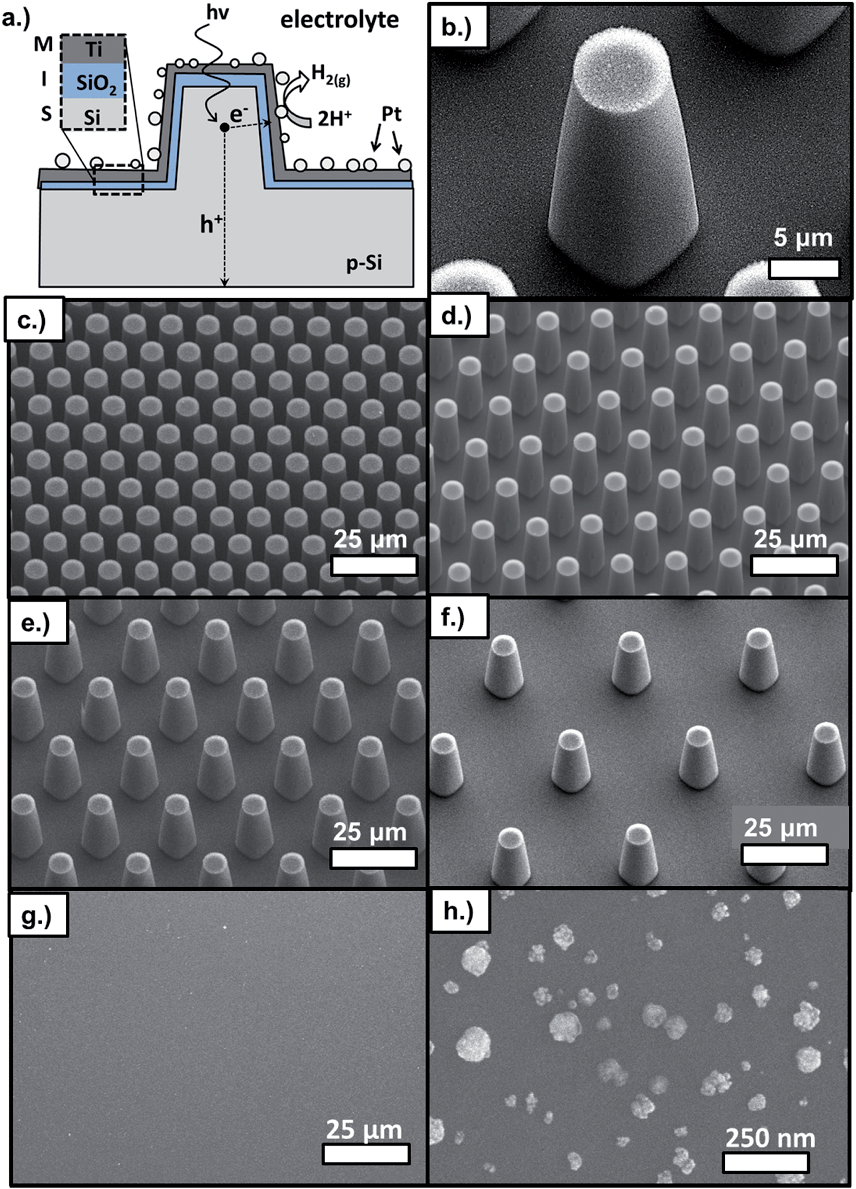 | ||
| Fig. 1 (a) Schematic side-view of a 3D metal–insulator–semiconductor (MIS) photocathode on which the hydrogen evolution reaction (HER) is taking place. (b–f) SEM images of a series of p-Si, MIS photocathodes consisting of arrays of micro-pillars fabricated by reactive ion etching (RIE). The pillar arrays in (c–f) consist of pillars with radii of 3 μm and varied pitch of (c) 11 μm, (d) 16 μm, (e) 23 μm, and (f) 38 μm. (g and h) SEM images of planar RIE photoelectrode lacking pillars. All scale bars shown in SEM images apply to the x dimension only. | ||
The RIE process produces uniform arrays of micro-pillars arranged in a close packed pattern, as seen in SEM images (Fig. 1c–f). Achieving a high degree of uniformity is important because it ensures that micro-scale measurements performed at one location of the sample are representative of the entire sample surface, allowing for comparison of locally-measured performance to macro-scale measurements. The critical geometric parameters of the Si micro-pillars are the diameter, pitch, and height (Fig. 1b). Fig. 1 shows SEM images for a series of samples that formed the basis of this study and consisted of pillars with top diameter of 6 μm, height of 27 μm, and pitch between 11 μm and 38 μm. For almost all samples, pillars did not have perfectly vertical sidewalls, but were slightly tapered with an angle between ≈3° and 8° with respect to the surface normal that decreased with increasing pillar density. Next, contamination was removed and surface roughness decreased by wet chemical treatment as described in Section IV. Following chemical treatment, a thin SiO2 insulating layer was grown by RTO at 950 °C in an N2/O2 environment. The low work function Ti layer was then deposited by e-beam evaporation, followed by electrodeposition of Pt catalyst particles. Although variation in particle size existed, electrodeposition produced a high density of nanoparticles on the pillar tops, side-walls, and basal areas (Fig. S4†). Typical Pt particle diameters ranged between 28 nm and 55 nm, and TEM images (Fig. S2†) showed that the particles exhibited a porous structure similar to that observed previously for electrodeposited Pt.35
Although the SEM images in Fig. 1 show good pillar to pillar uniformity, the RIE process causes etch damage that varies on surfaces of the pillar tops, pillar side walls, and basal regions between the pillars. As seen in TEM images (Fig. S2†), the surfaces of the pillar tops did not exhibit etch damage because they were protected by photoresist, but the surfaces of the pillar side-walls (Fig. S6†) and basal regions possessed a higher degree of nanoscale roughness. A second difference between the MIS junctions on the top, basal, and side-wall surfaces was the thickness of the Ti layer deposited by e-beam deposition. This Ti layer, which is partially oxidized to TiOx after exposure to air,27 is significantly thinner on portions of the side-wall surfaces due to parallax effects including self-shadowing from adjacent pillars. Despite planetary rotation of the samples during e-beam deposition, cross-sectional SEM measurements indicated that the thickness of the Ti layer is about 65% less on the pillar side-walls compared to the pillar tops (Fig. S3†). A third difference between pillar top, side-wall, and basal surfaces was the nature of the electrodeposited Pt particles. A relatively high density of Pt particles was obtained across much of the sample surface, although some variation in particle density and size exists on the pillar tops, side walls, and basal regions (Fig. S4†).
2.3 Current–potential performance of Si-based 3D MIS photoelectrodes
The performance of each photoelectrode was measured by linear sweep voltammetry (LSV) in deaerated 0.5 mol L−1 H2SO4 under simulated AM 1.5G illumination (Fig. 2). The LSV curve for a planar RIE control sample is also included. This planar sample underwent the identical processing steps as the other 3D samples except that it was not covered with patterned photoresist during the RIE process, resulting in a pillar-free surface having the same texture as the basal regions of the 3D-structured samples. Qualitatively, two major trends are evident in Fig. 2: (i) LSV curves shift to negative potentials as the pillar density increases and (ii) limiting current densities increase as the pillar density increases. In the remainder of this paper we use the methodologies described above to quantitatively evaluate the structure–property relationships that lead to the differences in performance seen in Fig. 2. | ||
| Fig. 2 LSV curves of p-Si MIS photocathodes shown in Fig. 1 and measured in deaerated 0.5 mol L−1 H2SO4 under simulated AM 1.5G illumination at 100 mV s−1. | ||
2.4 Modeling current–potential curves of 3D structured photoelectrodes
A model that can accurately describe the photocurrent versus electrochemical potential (E) behavior of a photoelectrode can serve as a useful framework for deconvoluting the various influences of 3D structure. For a well-behaved, illuminated junction, the starting point for this model is the diode equation,36 which describes the relationship between the current (I) passing through the junction and the voltage (V) across it: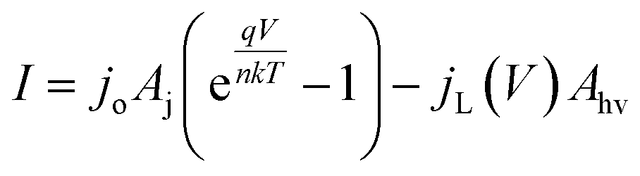 | (1) |
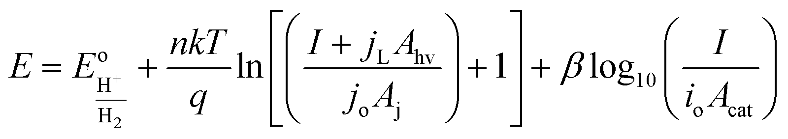
The diode equation accounts for carrier generation and collection, but it does not account for voltage losses associated with electrochemical charge transfer resistance, ohmic resistances, and more. In order to account for these losses, it is convenient to work with a model that treats current implicitly.38 This model describes the voltage difference between E, the potential applied to the Fermi level of the bulk semiconductor, and 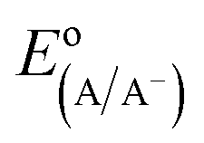 , the standard reduction potential of the half reaction taking place at the surface of the photoelectrode. For the hydrogen-evolving photocathodes being studied in this work,
  is given by:38
 | (2) |
 | (3) |
This current–potential (I–E) model will be used throughout the remainder of this paper as a framework for understanding the influence of 3D structure on photoelectrode properties and performance.
2.5 Effects of 3D structure on photoelectrode performance
 | (4) |
Because the silicon photoelectrodes used in this study are optically thick, T is close to zero across visible wavelengths, and the primary sources of optical losses are reflectance from the front surface of the photoelectrode and absorption of light by the Ti overlayer. When analyzing reflection losses, it is important to recall that optical reflectance may be specular or diffuse. When the angle of incidence (θi) is equal to the angle of reflection (θr), the reflection is characterized as specular, or “mirror-like” reflection. By contrast, diffusely reflected light is that for which θi does not equal θr, a situation that is often caused by scattering from front, back, or internal surfaces or internal scattering centers. Both types of reflection can be highly dependent on the wavelength-dependent indices of refraction of the constituent materials. However, it is well known that geometric factors, such as roughness, thickness, and shape, can also strongly influence optical properties.39 The size of 3D features is particularly important when the feature size becomes equal to or less than the wavelength of incident light because optical properties can be significantly altered at these length scales.40–42 For a perfectly flat single crystal electrode, almost all of the reflection is specular (Fig. 3a). However, light incident on a 3D-structured photoelectrode (Fig. 3b) may interact with the nano- or micro-structures on the surface, resulting in diffusely-reflected light.
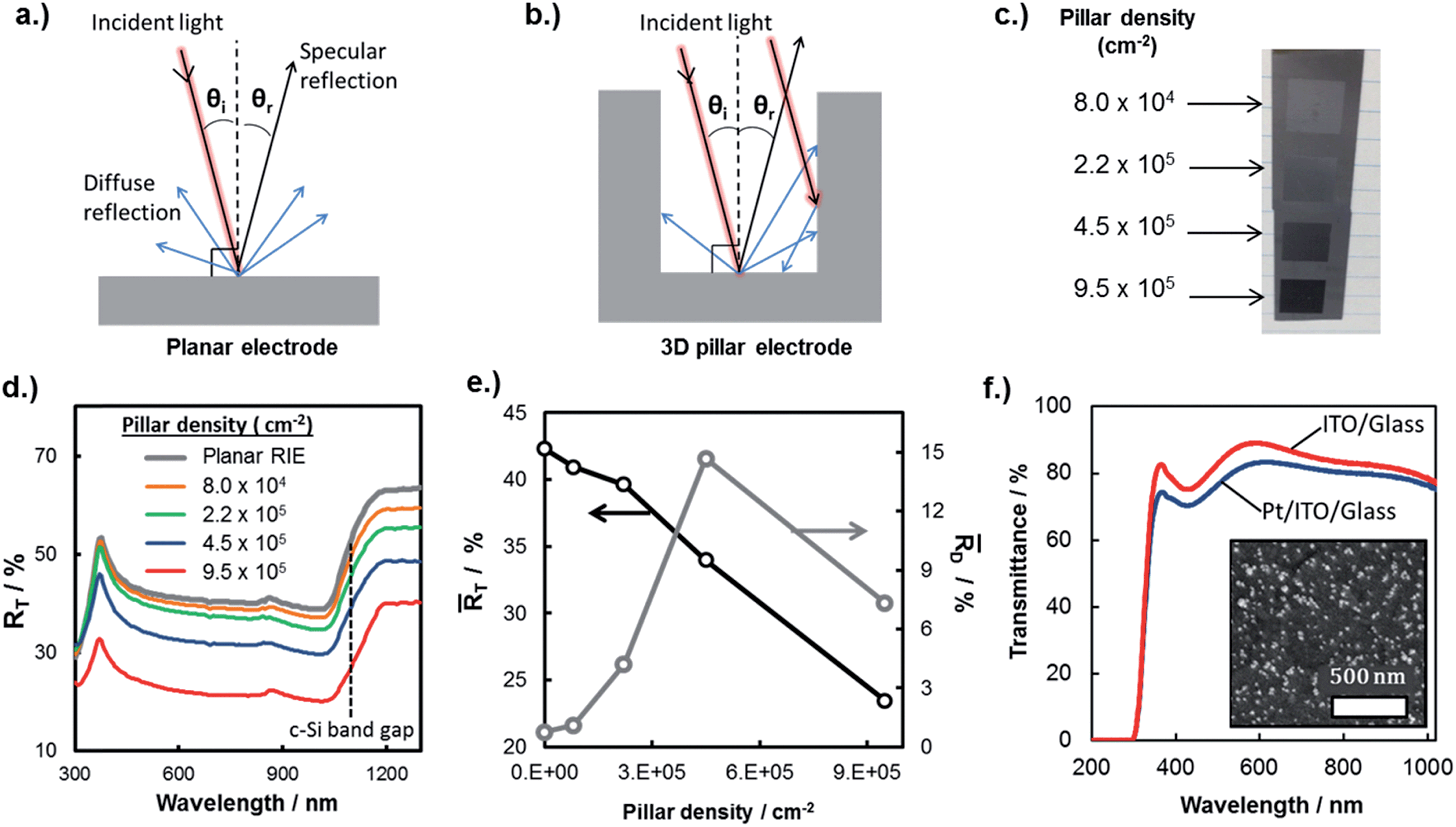 | ||
| Fig. 3 Optical properties of micropillar arrays. Schematic side-views of (a) planar and (b) 3D-structured photoelectrodes. (c) Photograph taken at an angle of ≈45° of four micropillar array samples from Fig. 2. Image (d) UV-Vis total reflectance (RT) spectra of planar and 3D-structured MIS samples from (c). (e) Average values of total reflectance (RT) and diffuse reflectance (RD) of samples in (c) between 400 nm to 700 nm. (f) Predicted change in limiting current due to 3D structuring based on UV-Vis data compared to the actual change in limiting current densities in the LSV curves in Fig. 2. | ||
In order to quantify the influence of 3D structuring on the optical reflectance, the reflectance properties of the photoelectrodes were measured by ultraviolet-visible (UV-Vis) spectroscopy. The total reflectance (RT) spectra of the 3D photoelectrodes, measured with an integrating sphere, are provided in Fig. 3d. These spectra show that the planar MIS electrode exhibits substantially higher reflectance across the entire range of wavelengths compared to the 3D structured samples. By measuring the specular reflectance (RS), the diffuse reflectance (RD) was also calculated. In Fig. 3e, the average values of RT and RD between 400 nm and 700 nm in Fig. 3d are plotted as a function of pillar density. RD is observed to initially increase with pillar density due to the increased light scattering off of the 3D structures. However, RD decreases for the sample with the largest pillar density because a high percentage of the photons that are diffusely reflected from the surface of the photoelectrode are absorbed by the closely-packed neighboring pillars. From Fig. 3e, the planar control sample has an average RT of 42% for normal incidence light, but this value drops to 24% for the sample with the highest pillar density. The difference in reflection is evident upon visual inspection of the samples at an angle of ≈45° (Fig. 3c), and becomes even more pronounced when the angle of incidence deviates from the surface normal (Fig. S7†). While the decrease in RT is significant for these micro-structured photoelectrodes, it should be noted that nano- or micro-structuring has been shown to reduce RT of photoelectrode13 and PV22,43 cell surfaces below 3%.
For all samples at normal incident illumination, the reflection losses predicated from UV-Vis reflectance measurements constitute a major source of photocurrent loss. However, the data shown in Fig. 3 overestimates the reflection losses that are incurred during photoelectrode operation, in which reflection occurs off of the electrolyte/photoelectrode interface instead of the air/photoelectrode surface. This difference in reflection results from differences in the indices of refraction, nr, of air and the aqueous electrolyte. As described by the Fresnel equations,44 reflectance at an interface is highly dependent on the difference in index of refraction values of the two materials forming that interface. While Si and the thin TiOx coating contain large indices of refraction, air has a very low index of refraction. Because the index of refraction of the aqueous electrolyte (nr ≈ 1.33)45 is larger than that of air (nr ≈ 1.00), reflection losses are lower during photoelectrode operation than the values provided in Fig. 3. Assuming that the Ti overlayer on the MIS photocathodes in this study have an index of refraction equal to that of anatase TiO2 (nr ≈ 2.52),46 the Fresnel equations predict that reflectance of normal incident light from a planar surface immersed in an aqueous electrolyte should be ≈49% lower than when the reflectance is measured in air.
Optical losses due to parasitic absorption can also impact photoelectrode performance. In the MIS photocathodes of this study, parasitic absorption losses may result from light absorption by the partially oxidized Ti overlayer, Pt nanoparticles, and the electrolyte. It has previously been shown that the absorption of light by aqueous electrolyte, especially at IR wavelengths, can be significant for photoelectrodes containing narrow band gap semiconductors.47 The p-Si photocathodes studied in this work only exhibit significant photoconversion at wavelengths from ≈300 nm to 900 nm (Fig. 6), a range in which the absorption of light by water is negligible at electrolyte thicknesses < 5 cm.47 In order to approximate the optical losses originating from the Pt co-catalysts, a control sample was fabricated in which Pt nanoparticles were electrodeposited onto a transparent glass substrate coated with a thin, conductive layer of indium tin oxide (ITO). As determined from SEM images of this sample (Fig. 3f inset), the 2D coverage of Pt nanoparticles on this sample (θPt ≈ 13%) was very similar to the coverage of Pt nanoparticles employed on the p-Si photoelectrodes used in this study. This sample thus offers a means of characterizing the optical losses that can be attributed to light blocking by the Pt nanoparticles. In Fig. 3f, the UV-Vis transmittance spectra for the Pt/ITO/glass sample is compared to that of a bare ITO/glass substrate, showing that the presence of the electrodeposited Pt nanoparticles decreased transmittance by an average of 5.5% (absolute) over the wavelength range between 400 nm and 700 nm. This value represents an upper limit on the amount of light blocked by the Pt nanoparticles, since some light scattered by the particles is not collected by the UV-Vis spectrometer in transmittance mode.
The parasitic absorption loss associated with light transmittance through the Ti overlayers was not directly measured in this study, but is also expected to contribute to the total optical losses. Because the precise composition of the partially oxidized Ti layer was not known, absorption losses could not be calculated using the Beer–Lambert law. Nonetheless, it is reasonable to assume that the absorption losses associated with the Ti overlayer are not greatly affected by 3D structure under normal incident illumination, since light must pass through Ti layers of similar thickness (≈15 nm) for both planar and 3D structured samples.
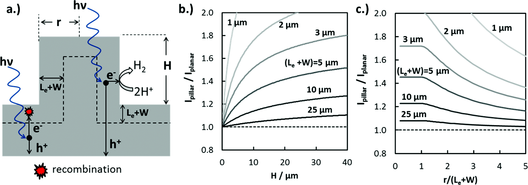 | ||
| Fig. 4 Modeled enhancement of carrier collection for AM 1.5G illumination. (a) Schematic side-view of micro-pillar illustrating enhanced charge carrier collection efficiency due to orthogonalization of light absorption and carrier collection in 3D structured photoelectrode. (b) Modeled enhancement of photocurrent in a c-Si micro-pillar under AM 1.5G illumination compared to a planar region (Ipillar/Iplanar) as a function of pillar height and carrier collection length (Le + W) assuming that r < (Le + W). (c) Modeled enhancement in photocurrent for c-Si micropillar as a function of dimensionless radius (r/(Le + W)) and carrier collection length for a constant pillar height of 25 μm. | ||
The increase in jL in 3D-structured photoelectrodes due to enhanced carrier collection is strongly dependent on the photoelectrode geometry, the wavelength of incident light, and the absorber layer properties such as absorption coefficient, α(λ), dopant density, and Le. Values of Le, defined as the average distance a minority carrier can travel before recombination takes place, can vary by orders of magnitude depending on the absorber material. Le can approach several mm for high-purity silicon wafers with low- to moderate doping levels,48 but Le values for oxide semiconductors are more commonly less than 50 nm due to charge localization and high intrinsic defect concentrations.49 In order to illustrate the influence of 3D structure and (Le + W) on enhanced carrier collection, the maximum expected photocurrent enhancement for cylindrical Si micropillars under normal incidence AM 1.5G irradiation was calculated numerically. For this analysis, photon absorption was modeled using the Beer–Lambert law and optical absorption coefficient data for c-Si.50 The IQE(λ) was set to 100% for photons absorbed within (Le + W) of the 3D junction and having energy greater than the bandgap of Si (Eg = 1.12 eV), and set to zero for all photons absorbed further than (Le + W) from the closest junction. Modeling IQE as a step function introduces some error in the predicted photocurrent, but still provides a useful basis for understanding trends in how enhanced carrier collection depends on 3D structure.
The ratio of photocurrent generated by light absorbed in a pillar structure relative to that for an identical planar surface illuminated with AM 1.5G light was modeled as a function of pillar height (Fig. 4b), as well as the dimensionless pillar radius, (r/(Le + W)) (Fig. 4c). In Fig. 4b, the photocurrent ratio, Ipillar/Iplanar, increases logarithmically with pillar height as an increasingly larger fraction of the carriers generated from long wavelength photons are collected at pillar side-walls. Ipillar/Iplanar is furthermore seen to be a strong function of (Le + W), especially for (Le + W) < 10 μm. This observation is consistent with a well-known generality in the solar PV and photoelectrochemistry fields: increase in photocurrent due to enhanced carrier collection in 3D structured solar cells and photoelectrodes is most significant for contaminated48 or low-quality materials having low Le.2 In Fig. 4c, the photocurrent enhancement is a constant for pillar radii r ≤ (Le + W), reflecting the fact that excessive micro- or nano-structuring of photoelectrode materials is not beneficial for carrier collection. However, radii that are significantly greater than (Le + W) result in decreased carrier collection because carriers generated at the center of the pillar are not able to reach the pillar top or sidewall.
From Fig. 4b and c, it is evident that Le is a critical design parameter in the fabrication of efficient 3D photoelectrodes because it determines the range of optimal pillar radii for enhanced carrier collection and the pillar height needed to achieve meaningful carrier collection at pillar sidewalls. Knowing the value of Le is thus of great utility in the successful design of efficient 3D photoelectrodes. In this work, scanning photocurrent microscopy (SPCM) based on focused 532 nm and 790 nm laser beams was used to determine Le for a planar RIE control sample. Values of Le = (12.1 ± 1.0) μm and (12.2 ± 0.9) μm were measured using the 532 nm and 790 nm lasers, respectively (Fig. S8†). Confidence intervals for Le values were calculated based on two-sided 95% confidence intervals. Based on a value of Le = 12.0 μm and pillar height of 27 μm, Fig. 4b predicts a local photocurrent enhancement of 19% for photons that are incident on the pillar tops. However, the basal regions in between the pillars do not benefit from enhanced carrier collection efficiencies. For the 3D photoelectrode with the highest density pillars investigated in this study, pillars cover 48% of the 2D surface, meaning that the benefit of enhanced carrier collection is predicted to increase the light-limiting photocurrent, jL, by ≈9% compared to the planar control sample.
Experimental determination of the extent of carrier collection enhancement was achieved with both macro- and micro-scale measurements. At the micro-scale, the carrier collection enhancement of individual Si micro-pillars at normal incident angle was measured with in situ SPCM using laser excitation at 532 nm and 790 nm. In these measurements, the focused laser beam locally produces photocurrent, which was measured as a function of laser beam position with respect to pillar features (Fig. 5a). Within a given sample, the basal regions between pillars are representative of a planar control because carriers generated from laser light incident on these areas travel parallel to the direction of illumination to be collected. SPCM was performed with two different lasers because the enhanced carrier collection due to 3D structuring is highly dependent on incident wavelength. The expected (modeled) wavelength dependence of the photocurrent enhancement (Ipillar/Ibase) is shown in Fig. 5b for c-Si micropillars (Le = 10 μm). Significant improvement in carrier collection is only expected for wavelengths greater than 700 nm, for which the absorption depth in c-Si begins to become comparable to Le. Thus, Fig. 5b predicts that there should be negligible photocurrent enhancement for the 532 nm laser when it is positioned over the pillar, but significant enhancement for longer wavelength light such as that from a 790 nm laser beam.
 | ||
| Fig. 5 Enhanced carrier collection measured by in situ SPCM. (a) Schematic of in situ SPCM measurement. (b) Ratio of modeled photocurrent for monochromatic light sources of different wavelengths absorbed through the top of the pillar (Ipillar) to that absorbed through the base (Ibase) as a function of c-Si pillar height. It is assumed that the pillar radius r < 2(Le + W). PEC SPCM images taken with (c) 790 nm and (d) 532 nm lasers (Po ≈ 4 μW). The color bar applies to both (c) and (d). PEC SPCM line scans using 790 nm and 532 nm laser beams over p-Si MIS micropillars having diameters of (e) 6 μm and (f) 28 μm at the tops of the pillars. All SPCM line scans were done with an applied potential of −50 mV vs. RHE in 0.5 mol L−1 H2SO4. | ||
SPCM photocurrent maps of a single 6 μm diameter micropillar, taken with 790 nm (Fig. 5c) and 532 nm (Fig. 5d) laser beams, clearly reveal wavelength-dependent photocurrent enhancement. As expected from Fig. 5b, almost no improvement in photocurrent is observed for local illumination of the pillar top with the 532 nm laser, for which the c-Si absorption depth at 532 nm ≈ 1 μm is much less than the carrier collection length, (Le + W). By contrast, pronounced improvement in photocurrent is observed for the SPCM map produced with the 790 nm laser beam, for which absorption depth at 790 nm ≈ 10 μm is similar to (Le + W), resulting in significant carrier collection through the pillar sidewalls, and thus an increase in the local photocurrent. This behavior is also observed in SPCM line scans taken across the same pillar (Fig. 5c). The slight increase in photocurrent at the edges of the pillar is due to light scattering off of the tapered pillar side walls and absorbed by adjacent pillars and base. Importantly, excellent quantitative agreement is seen between the measured photocurrent enhancement (Ipillar/Ibase) and that predicted in Fig. 5b, further confirming that the differences in photocurrent maps for 532 nm and 790 nm lasers reflect differences in carrier collection due to 3D structuring. Good agreement of SPCM results with modeling (Fig. 4c) was also observed when SPCM measurements were performed on larger pillar sizes to view the effect of pillar radius on the enhanced carrier collection behavior. As seen in the SPCM line scans over a 28 μm diameter pillar (Fig. 5f), a significant decrease in photocurrent is observed when the 790 nm laser beam is positioned at the center of the pillar where the distance from the sidewalls is greatest. This effect becomes more pronounced for even larger pillars, where the local photocurrent at the center of the pillar becomes similar to that generated off the pillar (Fig. S9†).
A more common, but less direct, means of viewing photocurrent changes due to enhanced carrier collection is to perform macroscopic external quantum efficiency (EQE) measurements on 3D structured and planar samples. In Fig. 6, EQE spectra measured at an applied potential of 0.0 V vs. RHE are shown for planar and 3D structured photoelectrodes. These curves reveal higher relative photocurrent for the 3D micropillar sample at longer wavelengths compared to the planar control sample, consistent with the SPCM results for 532 nm and 790 nm lasers in Fig. 5. In Fig. 6b, the increase in EQE(λ) for the 3D photoelectrode relative to the planar photoelectrode is shown as a function of wavelength. While negligible difference in EQE is observed for 532 nm light, the EQE increased by 35% for the 3D photoelectrode under 790 nm illumination. This relative increase in EQE at 790 nm for these macroscale measurements is less than the relative improvement in local photocurrent observed in the microscale SPCM measurements with the 790 nm laser (≈45% improvement), which can be attributed to the fact that the pillars only cover ≈48% of the 3D structured surface.
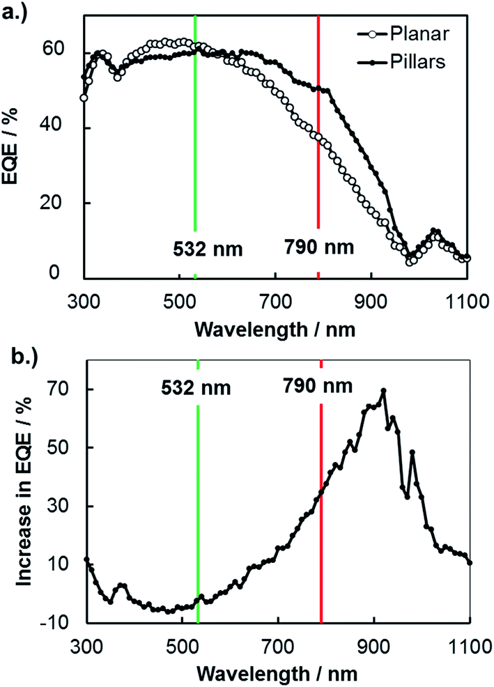 | ||
| Fig. 6 (a) EQE spectra for planar and 3D micropillar array electrodes in deaerated 0.5 mol L−1 H2SO4 under an applied potential of 0.0 V vs. RHE. (b) Percent increase in EQE(λ) for the 3D structured photoelectrode compared to the planar photoelectrode. | ||
An additional useful feature of the macroscopic EQE curves is that this data can be fit to the Gartner model to obtain an estimate of the effective minority carrier diffusion length.51 Performing this analysis on the EQE curves in Fig. 6 gives effective diffusion lengths of 11 μm and 22 μm for the planar and 3D structured samples, respectively. The value obtained for the planar photoelectrode is in good agreement with the value of Le obtained by SPCM line scans, but the value of Le for the 3D structured sample is significantly higher. This is because the fit to the macroscopic EQE curve gives an effective diffusion length that assumes a planar geometry for the sample. Stated otherwise, the 3D-structured sample is able to collect carriers as if it were a planar sample possessing an effective minority carrier diffusion length of 22 μm. However, the next section shows that the local minority carrier diffusion lengths in an individual micropillar are significantly less than this value.
In this work, the influence of surface recombination on 3D MIS photoelectrodes was investigated using electron beam induced current (EBIC) measurements in an ultra-high vacuum (UHV) environment. Fig. 7a contains a schematic side-view of the EBIC set-up used in this study, whereby the electron beam is injected into the top of the pillar and the electrical current measured between a probe contacting the pillar top and the back contact of the sample. Using this arrangement, current is measured as a function of the energy of the incident electron beam, which determines the absorption depth of the beam and thus the location of electron/hole pair generation with respect to the pillar top. Importantly, electrical characterization between the pillar tops and the basal regions immediately adjacent to the pillar revealed open-circuit behavior, indicating that the thin metal layer of the MIS structure is not continuous between the pillar tops, sidewalls, and the basal regions surround the pillars. A consequence of the discontinuous metal layer is that minority carriers generated far from the pillar top are not able to reach the current-collecting probe through conduction along the metal layer on the side-wall, but must travel up the pillar itself and cross the MIS junction at the pillar top. This carrier transport behavior is in contrast to a working device, in which the sidewalls are themselves current collectors through which minority carriers can be collected and directly transferred to oxidant species (H+) in the electrolyte through an electrochemical reaction.
 | ||
| Fig. 7 Analyzing surface recombination in micropillars with EBIC. (a) Schematic side-view of an EBIC measurement being performed on a micropillar. (b) Dependency of the collection probability, function ϕ(z), on beam position with respect to distance from the top of the pillar (z = 0). It is assumed that ϕ(z) = 0 in the interval [0, zd] (this is a thin, electrically inactive “dead” layer”), ϕ(z) = 1 in the interval [zd, W] (over the depletion width), and decays exponentially with length scale Le for z > W. Also shown are the generation rate profiles G(z) for two values of beam energy, as described in the text. We take G(z) = 0.6 + 6.21(z/z0) − 12.4(z/z0)2 + 5.69(z/z0)3,89 where the length scale z0 varies with electron beam energy as described in the text. (c) Collected EBIC current versus beam energy for a pillar with 15 μm diameter, compared with the data fit. Fit parameters are zd = 25 nm, W = 1 μm, and Le = (4.3 ± 0.4) μm. (d) Variation of the effective diffusion length with pillar diameter, both measured and obtained from fitting to eqn (5). | ||
The observed open circuit behavior in the UHV environment is useful for EBIC measurements because it enables one to determine the surface recombination velocity, S, of carriers at the sidewalls. In a working device where the sidewalls collect current, the surface recombination has little effect on jL. This is because the electric field associated with the Schottky contact is maximized near the sidewall, so that charges there are separated before they recombine. However, surface recombination is detrimental to open circuit voltage (Voc) because it increases dark current at forward bias. In the limit where the surface recombination velocity is much greater than both (W/τbulk) and the bulk diffusion velocity ( , where D is the minority carrier diffusivity), jo is proportional to S.53
The relative influence of bulk and surface recombination on the photovoltage varies with pillar diameter due to the changing ratio of the pillar surface area to the pillar volume. The effective carrier lifetime τeff is determined by solving the diffusion equation in a radial geometry as a function of radial position ρ, with the boundary condition that the radial diffusion current jρ at pillar radius r satisfies jρ(r) = S × n(r), where S is the surface recombination velocity, and n(r) is the electron concentration at ρ = r (see ESI for details†). This leads to:
 | (5) |
 .
.
Values of Le can be obtained from EBIC measurements using a least-squared fitting procedure based on the curves shown in Fig. 7b. This figure illustrates the spatial distribution of the generated excited electron–hole pairs, G(z), and the collection probability of an electron–hole pair as a function of the distance, z, that the exciton is generated from the collection probe. The total collected current is given by the product of these two functions. The electron–hole pair excitation profile is assumed to be known a priori (see caption of Fig. 7), and depends primarily on the electron beam energy: larger electron beam energies result in a spatial distribution of excited electron–hole pairs which penetrates deeper into the bulk. The relationship between the length scale of the excitation, z0, and the beam energy, Ebeam, is given by: z0 = 0.043 × C0/(ρ/ρ0) × (Ebeam/E0)1.75, where ρ is the mass density, ρ0 = 1 g cm−3, C0 = 1 μm is a constant, and E0 = 1 keV.54 The precise form of the generation profile is given in the caption of Fig. 7. By systematically varying the beam energy and measuring the current, the parameters describing the collection probability, such as Le, may be obtained through a least-squares fitting procedure. An example of one such fit is shown in Fig. 7c for a pillar with radius of 15 μm. The primary experimental uncertainty arises from variation in the collected current at the top of the pillar, which generally varies between 1% to 9%. There is also uncertainty in the modeling from the use of the empirical formula describing the generation profile of electron hole pairs. By comparing this empirical distribution to more accurate Monte Carlo models of electron beam induced electron–hole pair generation, we find that introducing a 5% uncertainty in the length scale of the excitation is appropriate. The ensuing uncertainty in Le is determined by performing fits using excitation length scales of z0 + 0.05z0 and z0 − 0.5z0.
This procedure was repeated for a series of pillars with varying radius, and the fitted values of Le are shown in Fig. 7d as a function of pillar radius. The uncertainties associated with the reported Le values arise from the uncertainty in the generation profile, as described above. Fig. 7d shows that the effective diffusion length decreases with decreasing radius, due to the enhanced influence of surface recombination as the surface area/bulk ratio increases. Performing a least-squares fitting procedure of eqn (5) to the data gives a surface recombination velocity of S = (8.5 ± 2.0) × 104 cm s−1. For reference, values of S between 50 cm s−1 and 500 cm s−1 have been commonly achieved for lightly doped p-Si wafers passivated by thermal SiO2, while values of S less than 10 cm s−1 have been achieved for more resistive Si wafers (>100 Ω cm) with thermally-grown SiO2 overlayers.55 The large value of S for the RIE-fabricated Si micropillars studied in this work underscores the importance of passivating the surfaces of the semiconductor in 3D structured photoelectrodes. In addition to rapid thermal annealing, two other common approaches to decreasing surface recombination velocities in Si solar cells include passivation by chemical vapor deposition of silicon nitride (SiNx) and the introduction of fixed charges near the Si interface to induce an inversion layer that repels majority carriers from that interface.55
 | (6) |
Within eqn (6), the sign in front of Voc is negative for photoanodes, and positive for photocathodes, while the sign of χ depends on the charge polarization associated with a given interface. Interfacial potential drops in photoelectrodes can originate from several different sources, including the electrochemical double layer,56 insulating dielectric or passivation layers,57,58 and surface dipoles associated with strongly bound adsorbates.59 Most often, χ does not intrinsically depend on 3D structuring or junction area, although processing involved with fabricating 3D-structured photoelectrodes can alter χ compared to a planar photoelectrode of the same material. By contrast, the total dark saturation current of a junction, jo,t = (jo × Aj), and thus its Voc, is highly dependent on the 3D area of the junction.2 This relationship between junction area (Aj) and Voc is observed by taking the diode equation (eqn (1)) at open circuit (I = 0 A) and solving for V = Voc:
 | (7) |
When [(jL × Ahv)/(jo × Aj)] ≫ 1, eqn (7) simplifies to:
 | (8) |
If χ = 0, then Eoc = Voc when referenced versus the reversible redox potential. For constant n and jo, eqn (8) predicts a linear relationship between Voc and ln(Aj/Ahv). Because (Aj/Ahv) is usually greater than one for 3D structured photoelectrodes, the photovoltage of a 3D structured photoelectrode will almost always be less than that which can be obtained for an otherwise identical planar sample for which (Aj/Ahv) = 1. This decrease in photovoltage due to 3D structuring is an inherent disadvantage of 3D structured photoelectrodes. Fig. 8a contains the experimentally measured Eoc values for our series of samples under 100 mW cm−2 intensity, along with modeled curves of Vocversus ln(Aj/Ahv) calculated from eqn (8) for n = 1.35 and jo = 1 × 10⁻⁸ A cm−2. For the experimental data, Aj was taken to be equal to the physical 3D area of the photoelectrode, A3D, which is calculated from the micropillar dimensions and the pillar packing densities. From Fig. 8a, good linearity is observed for the first four samples of the series, but the Eoc data point for the sample with the highest pillar density deviates substantially from this trend. This indicates that the effective n and/or jo of the highest pillar density sample are substantially different from the other samples. In order to verify this hypothesis, it follows from eqn (8) that n and jo for an individual sample can be estimated by plotting the measured Eocversus ln(jL), where jL is varied by adjusting the illumination intensity and Eoc is measured separately at the same intensity under open circuit conditions. From this plot (Fig. 8b), the values of n and jo for a given sample can be estimated from the slope and intercept, respectively. These values are plotted in Fig. 8c, revealing that both the n and jo values of the sample with the highest pillar density are indeed significantly higher than those of the planar and low-density pillar samples.
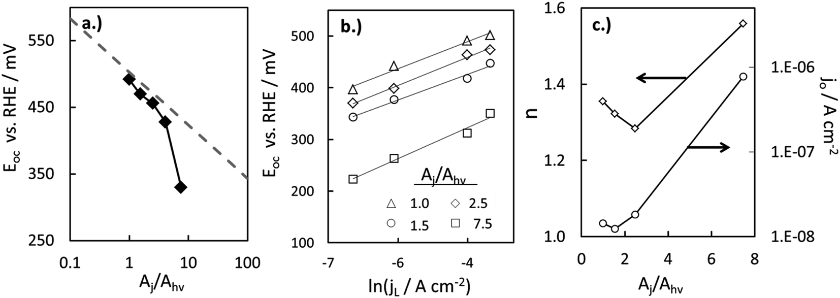 | ||
| Fig. 8 Variation in photovoltage with increased level of 3D structuring. (a) Experimental (solid diamonds) and calculated (dashed lines) values of open circuit potential (Eoc) as a function of the area ratio (Aj/Ahv). Calculated values of Eoc are based on eqn (6) for n = 1.35, jL = 22 mA cm−2, and jo = 1 × 10⁻⁸ A cm−2, where n and jo are taken from figure (c) for the planar sample. (b) Experimentally-measured Eoc values for a series of p-Si MIS photocathodes with varying Aj/Ahv at different illumination intensities. (c) Values of n and jo obtained from linear fits to the data in (b) based on eqn (6). jo in (c) is the dark saturation current density normalized by the net junction area of the electrode, Aj, which is assumed to be equal to the physical 3D surface area as estimated from SEM images. | ||
The variation in the n and jo values in Fig. 8c can most likely be attributed to (i) differences in local junction properties of pillar tops, pillar side walls, and basal areas and (ii) the fact that the relative surface areas of these junction types, Aji, vary significantly for the series of samples used in this study. For example, the sample with the highest pillar density also has the highest percentage of its total junction area located on pillar side walls. From high resolution SEM images, it is evident that pillar side-walls contain significantly higher roughness at the nanoscale, making it likely that the junction quality at the pillar side walls is significantly worse than the comparably smoother pillar tops and basal surfaces. Thus, it is not surprising that the analysis presented in Fig. 8 indicates that the high pillar density sample has the highest effective jo and n values, and that the Eoc of this sample is lower than one would predict from eqn (8) based solely on of its Aj/Ahv ratio.
In general, the influence of increased Acat on kinetic losses can be modeled with the Butler–Volmer equation, which describes the kinetically-limited current–potential (I–E) relationship for electrochemical charge transfer across an electrode surface. For electrochemical reactions in which the rate determining step involves the transfer of a single electron, the Butler–Volmer equation is:60
 | (9) |
 | (10) |
 | (11) |
Eqn (11) is a useful framework for highlighting some effects of 3D structure on photoelectrode current–potential (I–E) performance in well-controlled cases, but does have limitations. Notably, it does not account for mass transfer overpotentials, which are listed explicitly in eqn (3) but in practice are often difficult to deconvolute from kinetic overpotentials for fast reactions such as the hydrogen evolution reaction.63 For photoelectrodes operating under conditions where mass transport overpotential losses are likely to be significant, such as low reactant concentrations and/or ultra-low loadings of catalyst, the reader is referred to recent publications that discuss this topic in detail.64,65
The influence of catalytic properties on the current–potential (I–E) behavior of a photoelectrode is modeled in Fig. 9a, in which eqn (11) was used to model the LSV curves of a photocathode for four different values of (Acat/Ahv) and assuming that the surface contains a highly active catalyst with β = −40 mV per decade of current and io = 1 × 10⁻³ A cm−2. Values of (Acat/Ahv) less than one have been included to account for instances where the catalytically active sites do not cover the entire photoelectrode surface. With decreasing (Acat/Ahv), the LSV curve shifts to more negative potentials, reflecting the need for a larger kinetic overpotential in order to sustain a given photocurrent through a smaller catalytically active surface area. Conversely, increased (Acat/Ahv) shifts the LSV curve to positive potentials because the net photocurrent is distributed across more active sites such that a lower kinetic overpotential is required. For large loadings of highly active catalysts such as the blue curve in Fig. 9a, eqn (11) predicts an apparent increase in the photocurrent onset potential. However, such an observation is unlikely to be seen experimentally due to the occurrence of the back reaction, which was omitted from this analysis.
 | ||
| Fig. 9 Evaluating kinetic overpotential losses. (a) Modeled LSV curves based on eqn (11) for a photocathode with varied catalyst loading as described by the ratio (Acat/Ahv). The black line gives the solid-state IV curve characteristics based on the diode equation and using the following parameters: Aj = Ahv, jo = 1 × 10⁻¹⁰ A cm−2, n = 1.1, χ = 0, and jL = 25 mA cm−2. Kinetic overpotential losses were modeled based on Tafel kinetics using values of io = 1 × 10⁻³ A cm−2 and β = −40 mV per decade of current that are typical of a highly active HER catalyst such as Pt. The HOR back reaction has been ignored in this analysis, and the current has been normalized to the photoactive surface area, Ahv. (b) Modeled HER kinetic overpotential losses calculated as a function of (Acat/Ahv) using eqn (10) at constant (I/Ahv) = 10 mA cm−2. Curves are shown for the high activity catalyst from (a) and a lower activity HER catalyst characterized by io = 6 × 10⁻⁵ A cm−2 and β = −80 mV per decade of current. (c) Experimental IR-corrected LSV curves recorded in deaerated 0.5 mol L−1 H2SO4 for control samples consisting of varied loadings of Pt particles electrodeposited onto metallic p+Si substrates coated with 15 nm Ti. Inset shows the overpotential at 10 mA cm−2 as a function of catalyst surface area (Acat) normalized to the geometric electrode area (Ageo). | ||
While Fig. 9a illustrates the effect of the catalyst loading on ηcat, Fig. 9b illustrates the influence of the intrinsic activity of the catalyst that is deposited on the photoelectrode surface. In Fig. 9b, the kinetic overpotential losses at I = 10 mA cm−2 were modeled as a function of (Acat/Ahv) for electrode surfaces coated with highly active co-catalyst like Pt or less active HER co-catalyst such as Ni. There is a strong dependence of ηcat on Acat for both catalysts, but this dependence is greatest for the less active catalyst due to its larger Tafel slope. As noted by previous studies,2,66Fig. 9b illustrates how 3D structuring can be especially beneficial for decreasing kinetic losses of less active catalysts by supporting higher catalyst loadings without incurring unacceptable levels of optical losses associated with those catalysts.
In order to independently estimate the kinetic overpotential losses associated with the samples used in this study, control samples were fabricated by electrodepositing different loadings of Pt nanoparticle catalysts onto conductive, degeneratively-doped p+Si substrates that were first coated with a 15 nm Ti overlayer to mimic the surface of photoelectrodes. Because the substrate is degenerate, it is not photo-active, and serves as a conductive metallic substrate for which the IR-corrected LSV curve can be used to directly measure the kinetic overpotential losses at the electrode surface.21,67Fig. 9c contains the LSV curve for control samples with three different Pt loadings (Acat/Ageo), where the values of Acat were taken to be the electrochemically active surface area (ECSA) of the Pt catalysts as determined by analysis of the integrated hydrogen under potential deposition (Hupd) current from cyclic voltammetry (CV) curves. As expected from the Tafel equation and as seen in the inset of Fig. 9c, the kinetic overpotential at (I/Ageo) = 10 mA cm−2 decreases linearly with log(Acat/Ageo), although the dependence is fairly weak due to the relatively small absolute value of β for Pt HER catalysts.
Importantly, the high catalytic activity of Pt ensures that the Pt loading necessary to maintain low kinetic overpotential losses is well below levels that would block a significant fraction of incident light.64,68 Consistent with these prior studies, we found that 2D Pt particle coverage of only ≈9.4% was sufficient to maintain kinetic losses of ≈100 mV at 10 mA cm−2 on a p+Si electrode coated with 2 nm SiO2 and 15 nm Ti. For this reason, and because this topic has been evaluated in detail elsewhere,66 we did not compare the influence of catalyst loading on planar versus 3D structured photoelectrodes. Instead, the deposition time used to electrodeposit Pt catalyst was kept the same for all photoelectrode samples investigated in this study.
 | ||
| Fig. 10 Measuring bubble-induced photocurrent losses. (a and b) LSV curves measured at different scan rates in the presence and absence of surfactant for (a) planar and (b) 3D-structured Si photocathodes. Red curve: 20 mV s−1 in 0.5 mol L−1 H2SO4, black curve: 100 mV s−1 in 0.5 mol L−1 H2SO4, blue curve: 20 mV s−1 in 0.5 mol L−1 H2SO4 + surfactant. Arrows show the direction of the LSV scan. The 20 mV s−1 scans were scanned from negative to positive to ensure that a significant amount of bubbles were present at lower current densities. Insets show photographs of photoelectrode surfaces after LSV measurements (no surfactant), with the width of both exposed photoelectrodes being ≈1 cm. (c and d) Chronoamperometry measurements in the absence (open markers) and presence (solid markers) of surfactant. | ||
There are at least two mechanisms by which 3D-structuring can influence the coverage of bubbles on an electrode surface. The first relates to the wettability, or hydrophobic character, of the electrode surface. When the electrode surface is hydrophilic, the low solid–liquid surface tension results in a large bubble contact angle, defined as the angle between the solid–gas and liquid/gas interfaces with an apex at the triple-phase contact point. This large contact angle corresponds to a lower adhesion force to the electrode surface, and consequently leads to a lower average bubble departure diameter and average bubble coverage.74 3D structuring, or surface roughness, can influence the wettability of a surface and lead to significant deviation in the observed contact angles compared to the Young contact angle for a smooth surface.75 The relationship between 3D-structuring, or roughness, and wettability has been most commonly described by the Wenzel and Cassie–Baxter models. According to both models, surface roughness tends to make a hydrophobic surface more hydrophobic, and a hydrophilic surface more hydrophilic.76,77 These models and the general phenomena they describe are most commonly applied to the behavior of liquid droplets on a 3D structured surface, but many of the basic principles can also be extended to the inverse case of a gas bubble immersed in liquid solution and attached to a solid surface. In the Cassie–Baxter model, the interstitial spaces between 3D features on a surface are occupied by the same phase as the bulk fluid (i.e. liquid electrolyte in this study), and Wenzel behavior is characterized by instances when the droplet or bubble attached to the 3D structured surface extends down into the interstitial spaces.75
The physical constraints on bubble growth imposed by the geometry of the micro-pillar environment may also be an important factor for bubbles that nucleate in the basal regions. For example, the maximum achievable diameter of a spherical gas bubble that nucleates on the basal surface between pillars is limited by the pitch and diameter of adjacent pillars. Above this diameter, bubble detachment should be favored over continued growth whereby the bubble would have to contort itself into energetically-unfavorable shapes with high surface area to volume ratios. Bubble growth on pillar tops is also expected to experience geometric constraints that lead to enhanced detachment. For bubble nucleation on the top of a pillar, the maximum diameter of the base of the bubble, where it is attached to the electrode, is limited to the diameter of the pillar. As a bubble continues to grow, this constraint on the triple phase contact diameter necessitates a larger contact angle. According to the Young–Duprè equation, which describes the relationship between the liquid surface tension, contact angle and adhesion force of a bubble or droplet on a surface,78 this increase in contact angle should decrease the adhesion force, and therefore lead to bubble detachment at a smaller diameter than would be expected on an otherwise identical planar electrode. Coalescence of bubbles from the tops of neighboring pillars may also decrease bubble detachment diameters, as similarly observed for studies of disc electrodes of varied pitch.79 Overall, the combined effects of 3D surface morphology on bubble dynamics are expected to facilitate detachment of bubbles from the electrode surface, leading to lower bubble coverage on the surface and a smaller influence on photoelectrode performance.
In this study, the net influence of gaseous bubbles on the total photocurrent generated by a photoelectrode was measured by two commonly-used electroanalytical techniques: LSV and chronoamperometry (CA). When measured by LSV, the influence of bubbles can be viewed by changing the scan rate of the LSV curve or by adding a surfactant to the electrolyte. Scan rate, ν, influences bubble dynamics by affecting the total charge passed during the LSV measurement, and thus the total amount of gaseous H2 or O2 evolved. In Fig. 10a and b, LSV curves were recorded for planar and 3D photoelectrodes at two different scan rates. At the faster scan rate of 100 mV s−1, the short scan time limits the amount of H2 bubbles evolved, thereby minimizing their negative influence on the measured photocurrent. However, significantly more H2 bubbles are generated during the longer LSV measurements conducted at the slower scan rate of 20 mV s−1. For the planar sample (Fig. 10a), this lower scan rate results in significant decrease in reduction current density at all potentials due to the more substantial build-up of bubbles on the surface. By contrast, the scan rate has negligible influence on LSVs performed on the 3D structured sample (Fig. 10b), indicating that the H2 bubbles evolved from that surface under the slow scan rate had little influence on photoelectrode performance. For both samples, it should be noted that the oxidation peak observed at positive potentials in the LSV curves that were scanned from negative to positive potential is due to the hydrogen oxidation reaction.
Another means of altering the gas bubble dynamics on the electrode surface is by adding a surfactant to the electrolyte to decrease the surface tension at the liquid/vapor interface (γLV) and/or to alter nucleation rates.13,80,81 Referring again to the Young–Duprè equation, a decrease in γLV lowers the work of adhesion holding the bubble to the surface, consequently decreasing the average bubble size at which that adhesion force is exceeded by the buoyancy and/or hydrodynamic forces that lead to bubble detachment from the surface. In turn, the smaller bubble departure diameter results in a lower surface coverage of bubbles and therefore minimization of their adverse effects. Fig. 10a and b also contain LSV curves measured in the presence of a surfactant. During these measurements, a constant stream of small bubbles, barely visible to the naked eye, evolved from the photoelectrode surface with very low bubble coverage. For both the planar and 3D structured MIS photoelectrodes, the LSVs conducted at 20 mV s−1 in the presence of surfactant are very similar to the 100 mV s−1 scans carried out in the surfactant-free solution. The similarity of these two LSV curves for the planar electrode indicates that the scan rate of 100 mV s−1 was fast enough to avoid significant bubble-induced losses in the surfactant-free solution, verifying its use as a “bubble-free” control measurement in this study.
The effect of bubbles on photoelectrode surface can also be viewed during constant potential CA measurements performed with and without surfactant (Fig. 10c and d). Consistent with the LSV measurements in Fig. 10b, the CA curves performed at two different applied potentials for the 3D photoelectrode are nearly independent of the presence of surfactant, again highlighting the ability of the 3D structure to facilitate efficient transport of H2(g) away from the photoelectrode surface. Unlike the 3D structured photoelectrode, the photocurrents in the CA curves measured for the planar photoelectrode exhibit a strong dependence on the presence of the surfactant (Fig. 10c). With the surfactant present, H2 bubbles were observed to detach from the electrode surface almost immediately. Without surfactant, large H2 bubbles slowly grew on the photoelectrode, blocking an increasingly higher percentage of the electrode surface as the recorded photocurrent gradually decreased. Every 20 s to 30 s, the growing bubbles eventually coalesce, leading to their detachment from the electrode surface and resulting in a sharp increase in photocurrent as a portion of the photoelectrode is temporarily freed of bubbles. Although 3D structuring is not the only way to mitigate the detrimental effects of bubbles on a photoelectrode surface, these measurements clearly highlight an advantage of 3D structured electrodes and illustrate how gas bubbles can strongly influence the steady state performance of photoelectrodes.
2.6 Overall current–voltage loss analysis
By combining experimentally measured parameters with the modeling framework described in this paper, it is possible to estimate the losses associated with various factors (optical, bulk recombination, bubbles, kinetics) and compare these losses between photoelectrodes. These losses can be visualized using loss analysis diagrams, which display the voltage and current losses of the photoelectrode as a function of applied electrochemical potential. Similar loss-analysis diagrams, often referred to as polarization curve figures, are routinely used in the fuel cell field to illustrate the dependency of ohmic, kinetic, and mass transport losses on operating current.82–84 Such diagrams can be of great utility for comparing the magnitudes and types of efficiency losses between various electrodes.Fig. 11 contains loss analysis diagrams for the planar control sample (Fig. 11a) and the sample with the highest pillar density (Fig. 11), the two samples that exhibit the greatest differences in their LSV curves in Fig. 2. The current–voltage curves of the photoelectrodes were modeled based on eqn (3), and each of the loss “wedges” were calculated as described in Section XI of the ESI.† Parameters needed to model individual wedges, such as n and io for modeling the solid-state behavior, were obtained from experiments specifically designed to determine those parameters. Since the LSV curves in Fig. 2 were performed at relatively high scan rate so as to minimize the influence of gas bubbles, the bubble-induced current and overpotential losses have been omitted from this analysis. Further details of construction of the loss analysis figures are provided in Section XI of the ESI.†
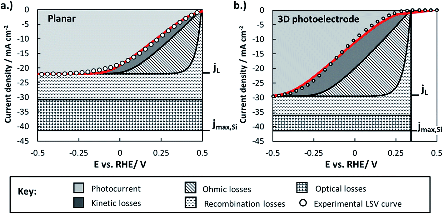 | ||
| Fig. 11 Loss analysis diagrams comparing losses in (a) the planar control photoelectrode and (b) the 3D structured photoelectrode with the highest pillar density. The solid red line represents the modeled LSV curve. jL is the photo-limiting current density, and jmax,Si is the maximum theoretical current density that can be achieved under AM 1.5G illumination. Solid-state losses refer to losses associated with bulk and surface recombination losses in the Si semiconductor and at the Si/SiO2 interface, respectively. | ||
Fig. 11 highlights several of the advantages and disadvantages of 3D structuring, and serves as a useful summary of many of the key findings regarding the p-Si photocathodes studied in this work:
(i) The light-limiting photocurrent density (jL) of the 3D structured photoelectrode increases by about 35% compared to the planar sample. As shown in Section 2.5.1, the main reason for this improvement in jL is an increase in optical absorption by the 3D structured photoelectrode due to decreased optical reflection losses. Enhanced carrier collection for minority carriers generated by long-wavelength photons in the 3D-structured photoelectrode also contributes to the increase in jL, but the analysis in Section 2.5.2 showed that the relative increase due to this influence should only be ≈9% (equivalent to 2 mA cm−2) for the high density pillar sample compared to the planar control. Nonetheless, it must be noted that the benefit of 3D structure on enhanced carrier collection will be much larger for photoelectrodes with low quality semiconductors that are characterized by smaller effective minority carrier diffusion lengths.
(ii) The higher junction area and lower junction quality of the 3D structured photoelectrode decreases its photocurrent onset potential by ≈250 mV compared to the planar sample due to the significant increase in the dark saturation current. This photovoltage loss is the single largest disadvantage of 3D structuring in this study, and the photovoltages recorded for all samples are significantly lower than the record photovoltage of 0.63 V that was recently demonstrated using n-Si MIS photoanodes.31 For reference, the world record Voc for a c-Si solar cell operated under AM 1.5 illumination is 0.706 V,85 very close to the theoretical maximum Voc ≈ 0.713 V that is calculated based on the bandgap of Si (Eg = 1.1 eV).86
(iii) Both samples suffered from significant ohmic losses. About 85–90% of the series resistance is attributed to the contact resistance associated with the indium solder back contact, with the remainder associated with the uncompensated solution resistance. The back contact resistance could be significantly reduced with low-resistance back contacts made by alloy formation or work function matching between the semiconductor and metallic back contact.
(iv) Good agreement between the experimental and modeled LSV curves is obtained for both the planar and 3D structured photoelectrodes, although some deviation exists at positive potentials for the latter. This disagreement may result from modeling the photoelectrode surface as a single homogeneous junction over its entire surface, whereas the local junction properties are likely to vary substantially between pillar tops, side-walls, and basal regions. For more complex 3D-structured photoelectrodes with disparate interfacial properties associated with different surfaces on the 3D features, it will likely be necessary to use numerical modeling and/or separate sets of equations for each region to explicitly account for these differences.
Collectively, the advantageous influences of 3D structure on photoelectrode performance were outweighed by its detrimental effects in this work. This outcome is exemplified by the fact that the IR-corrected photoelectrode conversion efficiency of the planar RIE sample was 5.8%, while that for the 3D structured photoelectrode was only 2.6% (see ESI Section X describing the calculation of photoelectrode efficiency†). This result underscores the important message that 3D structuring is not always beneficial, especially for semiconducting materials possessing effective minority carrier diffusion lengths that are similar to or greater than the optical absorption depth over most of the wavelength range of interest.
III. Conclusions
This study has demonstrated a systematic approach to deconvoluting the various influences of micro-scale 3D structure on the performance of p-Si MIS photocathodes. This approach was made possible by (i) synthesizing a series of samples with well-defined micropillar geometries, (ii) employing a suite of experimental measurements designed to isolate specific influences of 3D structure, and (iii) combining experiment with modeling to establish structure–property–performance relationships. Through this knowledge, a comprehensive current–potential model of photoelectrode performance was developed that can help to explain and predict the performance of 3D structured photoelectrodes compared to their planar counterparts. This model can be used to construct loss analysis diagrams for comparing loss mechanisms between samples and identifying opportunities for improved performance. Many of the tools and methods demonstrated in this paper can be extended to other photoelectrode materials and 3D electrode architectures, helping to accelerate the development and optimization of PEC technology.IV. Methods and materials
4.1 Fabrication
4.2 Characterization
Acknowledgements
The majority of this research was performed while D. V. E. and Y. L. held National Research Council Research Associateship Award positions at the National Institute of Standards and Technology. Y. L. also acknowledges support under the Cooperative Research Agreement between the University of Maryland and the National Institute of Standards and Technology Center for Nanoscale Science and Technology, award 70NANB10H193, through the University of Maryland. The authors acknowledge the assistance and support of the staff at the NIST Center for Nanoscale Science and Technology (CNST) NanoFab facility. A. A. T. acknowledges partial support by Science of Precision Multifunctional Nanostructures for Electrical Energy Storage (NEES), an Energy Frontier Research Center funded by the U.S. Department of Energy, Office of Science, and Office of Basic Energy Sciences under award DESC0001160. Sandia National Laboratories is a multi-program laboratory managed and operated by Sandia Corporation, a wholly owned subsidiary of Lockheed Martin Corporation, for the U.S. Department of Energy's National Nuclear Security Administration under contract DE-AC0494AL85000. The authors acknowledge Sandra Claggett and Igor Levin at NIST for assistance with TEM sample preparation and measurements, respectively.References
- M. Gratzel, Nature, 2001, 414, 338–344 CrossRef CAS PubMed.
- M. G. Walter, E. L. Warren, J. R. McKone, S. W. Boettcher, Q. X. Mi, E. A. Santori and N. S. Lewis, Chem. Rev., 2010, 110, 6446–6473 CrossRef CAS PubMed.
- Y. Tachibana, L. Vayssieres and J. R. Durrant, Nat. Photonics, 2012, 6, 511–518 CrossRef CAS.
- H. Ye, J. Lee, J. S. Jang and A. J. Bard, J. Phys. Chem. C, 2010, 114, 13322–13328 CAS.
- J. W. Lee, H. C. Ye, S. L. Pan and A. J. Bard, Anal. Chem., 2008, 80, 7445–7450 CrossRef CAS PubMed.
- J. M. Gregoire, C. Xiang, S. Mitrovic, X. Liu, M. Marcin, E. W. Conrnell, J. Fan and J. Jin, J. Electrochem. Soc., 2013, 160, F337–F342 CrossRef CAS.
- N. Lewis, Electrochem. Soc. Interface, 2013, 43–49 CAS.
- K. Sliozberg, D. Schaefer, T. Erichsen, R. Meyer, C. Khare, A. Ludwig and W. Schuhmann, ChemSusChem, 2015, 8, 1270–1278 CrossRef CAS PubMed.
- E. L. Warren, S. W. Boettcher, M. G. Walter, H. A. Atwater and N. S. Lewis, J. Phys. Chem. C, 2011, 115, 594–598 CAS.
- S. W. Boettcher, J. M. Spurgeon, M. C. Putnam, E. L. Warren, D. B. Turner-Evans, M. D. Kelzenberg, J. R. Maiolo, H. A. Atwater and N. S. Lewis, Science, 2010, 327, 185–187 CrossRef CAS PubMed.
- J. M. Spurgeon, H. A. Atwater and N. S. Lewis, J. Phys. Chem. C, 2008, 112, 6186–6193 CAS.
- M. H. Lee, K. Takei, J. J. Zhang, R. Kapadia, M. Zheng, Y. Z. Chen, J. Nah, T. S. Matthews, Y. L. Chueh, J. W. Ager and A. Javey, Angew. Chem., Int. Ed., 2012, 51, 10760–10764 CrossRef CAS PubMed.
- J. H. Oh, T. G. Deutsch, H. C. Yuan and H. M. Branz, Energy Environ. Sci., 2011, 4, 1690–1694 CAS.
- C. Liu, N. P. Dasgupta and P. Yang, Chem. Mater., 2014, 26, 415–422 CrossRef CAS.
- C. Cheng, H. Zhang, W. Ren, W. Dong and Y. Sun, Nano Energy, 2013, 2, 779–786 CrossRef CAS.
- S. Y. Noh, K. Sun, C. Choi, M. Niu, M. Yang, K. Xu, S. Jin and D. Wang, Nano Energy, 2013, 2, 351–360 CrossRef CAS.
- C.-Y. Lee, L. Wang, Y. Kado, R. Kirchgeorg and P. Schmuki, Electrochem. Commun., 2013, 34, 308–311 CrossRef CAS.
- X. B. Chen, S. H. Shen, L. J. Guo and S. S. Mao, Chem. Rev., 2010, 110, 6503–6570 CrossRef CAS PubMed.
- K. Sivula, F. Le Formal and M. Graetzel, ChemSusChem, 2011, 4, 432–449 CrossRef CAS PubMed.
- B. Liu, C.-H. Wu, J. Miao and P. Yang, ACS Nano, 2014, 8, 11739–11744 CrossRef CAS PubMed.
- Y. W. Chen, J. D. Prange, S. Duhnen, Y. Park, M. Gunji, C. E. D. Chidsey and P. C. McIntyre, Nat. Mater., 2011, 10, 539–544 CrossRef CAS PubMed.
- J. Liu, B. W. Liu, S. Liu, Z. N. Shen, C. B. Li and Y. Xia, Surf. Coat. Technol., 2013, 229, 165–167 CrossRef CAS.
- M. J. Kenney, M. Gong, Y. Li, J. Z. Wu, J. Feng, M. Lanza and H. Dai, Science, 2013, 342, 836–839 CrossRef CAS PubMed.
- J. C. Hill, A. T. Landers and J. A. Switzer, Nat. Mater., 2015, 14, 1150–1155 CrossRef CAS PubMed.
- A. J. Nozik and R. Memming, J. Phys. Chem., 1996, 100, 13061–13078 CrossRef CAS.
- T. Zhu and M. N. Chong, Nano Energy, 2015, 12, 347–373 CrossRef CAS.
- D. V. Esposito, I. Levin, T. P. Moffat and A. A. Talin, Nat. Mater., 2013, 12, 562–568 CrossRef CAS PubMed.
- A. G. Munoz and H. J. Lewerenz, ChemPhysChem, 2010, 11, 1603–1615 CrossRef CAS PubMed.
- H. J. Lewerenz, K. Skorupska, A. G. Munoz, T. Stempel, N. Nusse, M. Lublow, T. Vo-Dinh and P. Kulesza, Electrochim. Acta, 2011, 56, 10726–10736 CrossRef CAS.
- A. G. Scheuermann, K. W. Kemp, K. Tang, D. Q. Lu, P. F. Satterthwaite, T. Ito, C. E. D. Chidsey and P. C. McIntyre, Energy Environ. Sci., 2016, 9, 504–516 CAS.
- A. G. Scheuermann, J. P. Lawrence, K. W. Kemp, T. Ito, A. Walsh, C. E. D. Chidsey, P. K. Hurley and P. C. McIntyre, Nat. Mater., 2016, 15, 99–105 CrossRef CAS PubMed.
- N. Y. Labrador, X. Li, Y. Liu, J. T. Koberstein, R. Wang, H. Tan, T. P. Moffat and D. V. Esposito, Nano Lett., 2016, 16, 6452–6459 CrossRef CAS PubMed.
- R. Singh, M. A. Green and K. Rajkanan, Sol. Cells, 1981, 3, 95–148 CrossRef CAS.
- R. B. Godfrey and M. A. Green, Appl. Phys. Lett., 1978, 33, 637–639 CrossRef CAS.
- J. Ustarroz, T. Altantzis, J. A. Hammons, A. Hubin, S. Bals and H. Terryn, Chem. Mater., 2014, 26, 2396–2406 CrossRef CAS.
- M. X. Tan, P. E. Laibinis, S. T. Nguyen, J. M. Kesselman, C. E. Stanton and N. S. Lewis, Prog. Inorg. Chem., 1994, 41, 21–144 CrossRef CAS.
- X. X. Liu and J. R. Sites, J. Appl. Phys., 1994, 75, 577–581 CrossRef CAS.
- R. H. Coridan, A. C. Nielander, S. A. Francis, M. T. McDowell, V. Dix, S. M. Chatman and N. Lewis, Energy Environ. Sci., 2015, 8, 2886–2901 CAS.
- M. D. Kelzenberg, S. W. Boettcher, J. A. Petykiewicz, D. B. Turner-Evans, M. C. Putnam, E. L. Warren, J. M. Spurgeon, R. M. Briggs, N. S. Lewis and H. A. Atwater, Nat. Mater., 2010, 9, 368–368 CrossRef CAS.
- L. Y. Cao, J. S. White, J. S. Park, J. A. Schuller, B. M. Clemens and M. L. Brongersma, Nat. Mater., 2009, 8, 643–647 CrossRef CAS PubMed.
- S. J. Kim, I. Thomann, J. Park, J.-H. Kang, A. P. Vasudev and M. L. Brongersma, Nano Lett., 2014, 14, 1446–1452 CrossRef CAS PubMed.
- S. Hu, C.-Y. Chi, K. T. Fountaine, M. Yao, H. A. Atwater, P. D. Dapkus, N. S. Lewis and C. Zhou, Energy Environ. Sci., 2013, 6, 1879–1890 CAS.
- J. Oh, H. C. Yuan and H. M. Branz, Nat. Nanotechnol., 2012, 7, 743–748 CrossRef CAS PubMed.
- J. M. Bennett, in Handbook of Optics, ed. M. Bass and V. N. Mahajan, McGraw Hill, 3rd edn, 2010, vol. 1, ch. 12, p. 31 Search PubMed.
- Index of refraction of inorganic liquids, in CRC Handbook of Chemistry and Physics, ed. W. M. Haynes, D. R. Lide and T. J. Bruno, CRC Press, Taylor and Francis Group, LLC, 97th edn, 2016, ch. section 4, p. 132 Search PubMed.
- Physical and optical properties of minerals, in CRC Handbook of Chemistry and Physics, ed. W. M. Haynes, D. R. Lide and T. J. Bruno, CRC Press, Taylor and Francis Group, LLC, 97th edn, 2016, ch. section 4, pp. 133–138 Search PubMed.
- H. Doscher, J. F. Geisz, T. G. Deutsch and J. A. Turner, Energy Environ. Sci., 2014, 7, 2951–2956 CAS.
- A. Boukai, P. Haney, A. Katzenmeyer, G. M. Gallatin, A. A. Talin and P. Yang, Chem. Phys. Lett., 2011, 501, 153–158 CrossRef CAS.
- S. Lany, J. Phys.: Condens. Matter, 2015, 27, 283203 CrossRef PubMed.
- M. A. Green and M. J. Keevers, Prog. Photovoltaics, 1995, 3, 189–192 CAS.
- J. R. McKone, A. P. Pieterick, H. B. Gray and N. S. Lewis, J. Am. Chem. Soc., 2013, 135, 223–231 CrossRef CAS PubMed.
- B. M. Kayes, H. A. Atwater and N. S. Lewis, J. Appl. Phys., 2005, 97, 114302 CrossRef.
- S. J. Fonash, J. Appl. Phys., 1980, 51, 2115–2118 CrossRef.
- A. E. Grün, Zeitschrift für Naturforschung A, 1957, 12, 89 CrossRef.
- A. G. Aberle, Prog. Photovoltaics, 2000, 8, 473–487 CAS.
- R. Memming, Semiconductor Electrochemistry, Wiley, 2001 Search PubMed.
- A. G. Scheuermann, J. D. Prange, M. Gunji, C. E. D. Chidsey and P. C. McIntyre, Energy Environ. Sci., 2013, 6, 2487–2496 CAS.
- B. Seger, S. D. Tilley, T. Pedersen, P. C. K. Vesborg, O. Hansen, M. Graetzel and I. Chorkendorff, J. Mater. Chem. A, 2013, 1, 15089–15094 CAS.
- W. A. Smith, I. D. Sharp, N. Strandwitz and J. Bisquert, Energy Environ. Sci., 2015, 8, 2851–2862 CAS.
- A. J. Bard and L. R. Faulkner, in Electrochemical Methods, John Wiley & Sons, Inc., 2nd edn, 2001, ch. 3, pp. 87–136 Search PubMed.
- C. C. L. McCrory, S. Jung, J. C. Peters and T. F. Jaramillo, J. Am. Chem. Soc., 2013, 135, 16977–16987 CrossRef CAS PubMed.
- C. C. L. McCrory, S. Jung, I. M. Ferrer, S. M. Chatman, J. C. Peters and T. F. Jaramillo, J. Am. Chem. Soc., 2015, 137, 4347–4357 CrossRef CAS PubMed.
- W. C. Sheng, H. A. Gasteiger and Y. Shao-Horn, J. Electrochem. Soc., 2010, 157, B1529–B1536 CrossRef CAS.
- Y. Chen, K. Sun, H. Audesirk, C. Xiang and N. S. Lewis, Energy Environ. Sci., 2015, 8, 1736–1747 CAS.
- E. Kemppainen, A. Bodin, B. Sebok, T. Pedersen, B. Seger, B. Mei, D. Bae, P. C. K. Vesborg, J. Halme, O. Hansen, P. D. Lund and I. Chorkendorff, Energy Environ. Sci., 2015, 8, 2991–2999 CAS.
- C. W. Roske, E. J. Popczun, B. Seger, C. G. Read, T. Pedersen, O. Hansen, P. C. K. Vesborg, B. S. Brunschwig, R. E. Schaak, I. Chorkendorff, H. B. Gray and N. S. Lewis, J. Phys. Chem. Lett., 2015, 6, 1679–1683 CrossRef CAS PubMed.
- S. Hu, M. R. Shaner, J. A. Beardslee, M. Lichterman, B. S. Brunschwig and N. S. Lewis, Science, 2014, 344, 1005–1009 CrossRef CAS PubMed.
- L. Ji, M. D. McDaniel, S. Wang, A. B. Posadas, X. Li, H. Huang, J. C. Lee, A. A. Demkov, A. J. Bard, J. G. Ekerdt and E. T. Yu, Nat. Nanotechnol., 2015, 10, 84–90 CrossRef CAS PubMed.
- A. Berger and J. Newman, J. Electrochem. Soc., 2014, 161, E3328–E3340 CrossRef CAS.
- S. Hernandez, G. Barbero, G. Saracco and A. L. Alexe-Ionescu, J. Phys. Chem. C, 2015, 119, 9916–9925 CAS.
- C. Sillen, E. Barendrecht, L. J. J. Janssen and S. J. D. Vanstralen, Int. J. Hydrogen Energy, 1982, 7, 577–587 CrossRef CAS.
- D. Fernandez, P. Maurer, M. Martine, J. M. D. Coey and M. E. Moebius, Langmuir, 2014, 30, 13065–13074 CrossRef CAS PubMed.
- H. Vogt, Electrochim. Acta, 1989, 34, 1429–1432 CrossRef CAS.
- K. Zeng and D. Zhang, Prog. Energy Combust. Sci., 2010, 36, 307–326 CrossRef CAS.
- A. Marmur, Soft Matter, 2006, 2, 12–17 RSC.
- R. N. Wenzel, Ind. Eng. Chem., 1936, 28, 988–994 CrossRef CAS.
- A. B. D. Cassie and S. Baxter, Trans. Faraday Soc., 1944, 40, 0546–0550 RSC.
- M. E. Schrader, Langmuir, 1995, 11, 3585–3589 CrossRef CAS.
- C. Brussieux, P. Viers, H. Roustan and M. Rakib, Electrochim. Acta, 2011, 56, 7194–7201 CrossRef CAS.
- Q. Chen, L. Luo, H. Faraji, S. W. Feldberg and H. S. White, J. Phys. Chem. Lett., 2014, 5, 3539–3544 CrossRef CAS PubMed.
- L. King and S. S. Sadhal, Heat Mass Transfer, 2014, 50, 373–382 CrossRef CAS.
- S. Park, Y. Shao, R. Kou, V. V. Viswanathan, S. A. Towne, P. C. Rieke, J. Liu, Y. Lin and Y. Wang, J. Electrochem. Soc., 2011, 158, B297–B302 CrossRef CAS.
- P. P. Mukherjee, Q. Kang and C.-Y. Wang, Energy Environ. Sci., 2011, 4, 346–369 CAS.
- M. K. Debe, Nature, 2012, 486, 43–51 CrossRef CAS PubMed.
- M. A. Green, Prog. Photovoltaics, 2009, 17, 183–189 CAS.
- M. A. Green, in Solar Cells, ed. J. Nick Holonyak, Prentice-Hall, Inc., Englewood Cliffs, N.J., 1982, pp. 85–102 Search PubMed.
- D. V. Esposito, O. Y. Goue, K. D. Dobson, B. E. McCandless, J. G. G. Chen and R. W. Birkmire, Rev. Sci. Instrum., 2009, 80, 125107 CrossRef PubMed.
- H. J. Leamy, J. Appl. Phys., 1982, 53, R51–R80 CrossRef CAS.
- T. E. Everhart and P. H. Hoff, J. Appl. Phys., 1971, 42, 5837–5846 CrossRef CAS.
Footnotes |
| † Electronic supplementary information (ESI) available. See DOI: 10.1039/c6se00073h |
| ‡ These authors contributed equally to this work. |
| This journal is © The Royal Society of Chemistry 2017 |