Lead-free pseudo-three-dimensional organic–inorganic iodobismuthates for photovoltaic applications†
Received
19th November 2016
, Accepted 13th January 2017
First published on 16th January 2017
Abstract
Two organic–inorganic iodobismuthates, C5H6NBiI4 ([py][BiI4]) and C6H8NBiI4 ([mepy][BiI4]), have been prepared with their structures revealed by single-crystal X-ray diffraction. One-dimensional BiI4− anionic chains built by edge-sharing BiI6 octahedra were found in both materials; short I⋯I, I⋯C contacts and hydrogen bonding give rise to three-dimensional intermolecular interactions. Both compounds are semiconductors, with band gaps of around 2.0 eV, and the contribution from the organic moieties to the conduction band minimum has been derived by density functional theory. Solid-state optical and electrochemical studies performed on powders and thin films were carried out, and their stabilities under an ambient environment have been demonstrated. Their use as the absorber layer in printable mesoscopic solar cells without any hole transport material has led to efficiencies up to 0.9%, showing a promising new approach towards the development of lead-free third-generation photovoltaic materials.
Introduction
During the last few years, the rapid emergence of organic–inorganic metal halide perovskite solar cells has led to a new era of research into solar energy utilization.1–9 Lead-based perovskite solar cells have been extensively studied, and are central to the extraordinarily rapid progress of power-conversion efficiency (PCE) from 3.8% in 2009 (ref. 1) to more than 20% today.8,9 Crucially, this is achieved via low-cost perovskite material preparation and facile fabrication, making them promising in the future photovoltaic market. However, one fact that may hinder the full application of this kind of metal–halide solar cell is the toxicity of lead. Concerns over the leakage of lead and the improper disposal of cells may restrict application in certain areas. To address the toxicity issue, developments in non-toxic metal–halide photovoltaics are now being explored. Tin, also a group 14 element with a similar atomic radius, has recently been studied to substitute lead within novel photovoltaic absorber materials. Perovskites including CH3NH3SnX3 (X = Cl, Br, I) and Cs3SnX3 (X = Br, I) in solar cell devices have achieved more than 6% PCE.10–12 However, tin-based perovskites exhibit extreme sensitivity to humidity and oxygen, which is a severe hindrance for their further application. Alternatively, bismuth–halide compounds have been proven to exhibit a photovoltaic effect,13–19 with PCE over 1% achieved for Cs3Bi2I9 (ref. 17) and for AgBi2I7.19 In all the solar cell applications mentioned above, a FTO/TiO2/perovskite/hole-transport material (HTM)/gold classical structure was adopted, which suffers a lot from the high cost of HTM and gold counter electrode.
In general, iodobismuthates have attracted attention due to their semiconducting properties, non-toxicity, air stability and solution processability. Great structural diversity of the anionic iodobismuthate motif can be found, ranging from the simplest [BiI6]3− to the poly-nuclear [Bi8I30]6−.20 Most iodobismuthate structures are built from zero-dimensional Bi/I anions. Among them [Bi2I9]3− complexes have been extensively investigated, including their crystal structures, optical properties and quantum physical properties.20–23 Different cations including CH3NH3+,14,15,24, NH4+,23 Cs+,18,22,25 Rb+,26,27 and K+ (ref. 27) have been studied, which may be used to aid the rational design of photovoltaics. So far, much focus has been put on the zero-dimensional [Bi2I9]3− structural unit in solar cells. Low dimensional materials are likely to give rise to limited capability for charge carrier transport, leading to relatively low PCE. We propose that alongside the well-studied zero-dimensional [Bi2I9]3− complexes, the lesser-studied iodobismuthates based on extended inorganic networks are also important candidates to explore for lead-free solar absorbers, such as 1D infinite chain structures, including [Bi2I72−]n, [Bi3I112−]n, [BiI4−]n, and [BiI52−]n.28–32
In this article, two organic–inorganic iodobismuthates, [py][BiI4] and [mepy][BiI4], featuring one-dimensional [BiI4]− anionic chain structures have been synthesised and studied. Compared to the work of Yelovik et al.,30 where the inorganic cations have almost no electronic interaction with the 1D BiI4− framework, we have demonstrated that the organic entities play an active role in intermolecular interactions and the frontier orbital, which makes them pseudo-3D materials regarding the dimension of charge transfer. Moreover, we have made cost-effective solar cell devices adopting an HTM-free mesoscopic structure with a carbon counter electrode, reaching the best efficiency of 0.9%. In this initial study, we show this approach as a new strategy towards the development of higher-dimensionality iodobismuthate frameworks, which presents a comparable order of magnitude of efficiency with the other best iodobismuthate examples.
Results and discussion
Crystal structures and intermolecular interactions
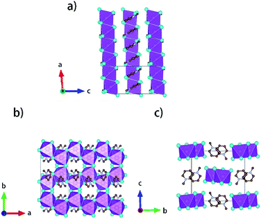
Single crystals of [py][BiI4] and [mepy][BiI4] were obtained at the interface of BiI3 ethanol solution and (methyl)pyridinium iodide water solution. Red plate-shaped [py][BiI4] and block-shaped [mepy][BiI4] were formed after a few days. From the single crystal XRD, both [py][BiI4] and [mepy][BiI4] consist of one-dimensional edge-sharing chains composed of BiI6 octahedra with the space group P21/c, while the difference in chain positions within the unit cell and the packing motif of the organic cations lead to the differences between their crystal structures. The general crystallographic packing for [py][BiI4] is shown in Fig. 1, displaying an inorganic framework built by [BiI4]− anionic chains with bridging cis-iodides. The Bi–I bond lengths are shorter (2.9047(19) Å – 3.0556(19) Å) for the terminal iodine atoms than for bridging iodine atoms (3.1326(19) Å – 3.2878(18) Å) in each BiI6 octahedron. The bond angles for I–Bi–I range from 84.75(5)° to 95.38(6)°, and the angles of I (bridging)–Bi–I (bridging) in each BiI6 octahedron are generally smaller than those of I (terminal)–Bi–I (terminal). The deviation of the geometric parameters indicates that the BiI6 octahedron is distorted, which is a common characteristic of iodobismuthates.24,33 In [mepy][BiI4], [BiI4]− anionic chains propagate along the a-axis with methylpyridinium cations arranged along the edge-sharing BiI6 chain direction. Shorter bond lengths for the Bi–I bond (2.9098(8) Å – 2.9195(8) Å) are again found for the terminal iodine atoms than that with bridging iodine atoms (3.1027(9) Å – 3.3029(7) Å) in the slightly distorted BiI6 octahedra. The bond angles for I–Bi–I range from 87.620(19)° to 94.30(2)° with smaller I (bridging)–Bi–I (bridging) than that with terminal I. Bi–I (bridging)–Bi angles range from 92.21(2)° to 93.75(2)°. The distortion of BiI6 octahedra in the two title iodobismuthate compounds probably originates from the repulsion of bismuth atoms between the adjacent [BiI6]3− building blocks (Fig. 2).24
 |
| | Fig. 1 Crystallographic packing diagrams of [py][BiI4] when viewed along different axes. Bismuth atoms and [BiI6]3− octahedra: magenta; iodine atoms: cyan; carbon atoms: brown; nitrogen atoms: violet. Hydrogen atoms are hidden for clarity. | |
 |
| | Fig. 2 Crystallographic packing diagrams of [mepy][BiI4] when viewed along different axes. Bismuth atoms and [BiI6]3− octahedra: magenta; iodine atoms: cyan; carbon atoms: brown; nitrogen atoms: violet. Hydrogen atoms are hidden for clarity. | |
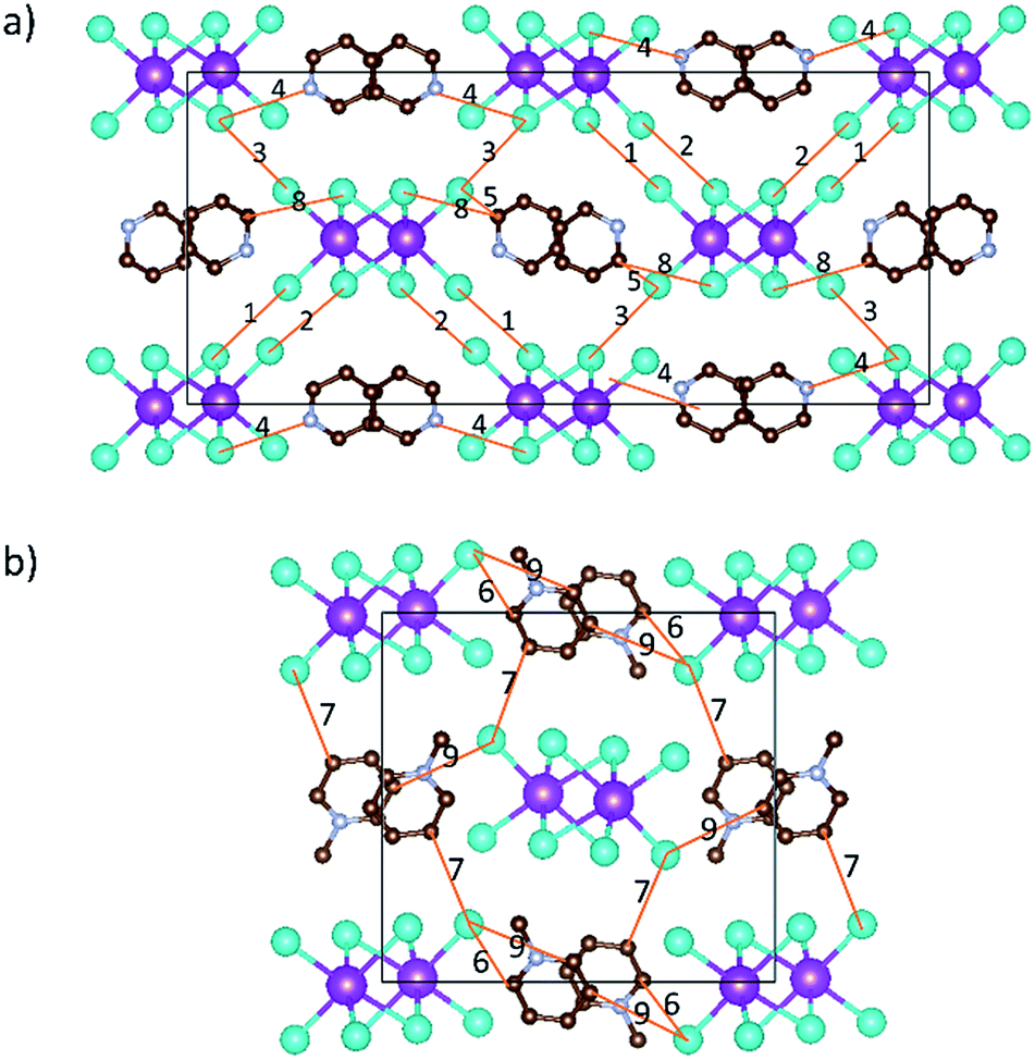
Interesting features for both compounds regarding intermolecular interactions can be observed when viewing along different axes (Fig. 3, S1 and S2†), and the corresponding short contact distances are listed in Table 1. In the crystal structure of [py][BiI4], short I⋯I contacts exist between two adjacent [BiI4]− chains in the ab plane, where the shortest distance (3.823 Å) is less than the sum of their van der Waals radii (3.98 Å). Hydrogen bonding with iodine and van der Waals interactions between iodine–iodine and iodine–carbon can also be found when viewed along the a- or c-axis (Fig. 3 and S1†). However, less intermolecular interactions can be observed in [mepy][BiI4]. There are short I⋯C contacts between the terminal iodine atoms and carbon atoms of the methylpyridinium rings, and hydrogen bonding involving the terminal iodine atoms runs perpendicular to the chain plane. Compared to [py][BiI4], no short I⋯I contacts were found. This can be attributed to the methyl group on the organic cation, which increases the volume of the organic component, increasing the distance between the anionic chains.
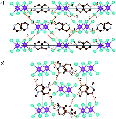 |
| | Fig. 3 Intermolecular interactions (shown in orange lines) in [py][BiI4] (a) and [mepy][BiI4] (b) unit cells. Image generated by VESTA (Visualization for Electronic and STructural Analysis) software. Bismuth atoms: magenta; iodine atoms: cyan; carbon atoms: brown; nitrogen atoms: violet. Hydrogen atoms are hidden for clarity. | |
Table 1 Short contacts of I⋯I, I⋯C, I⋯H–N and I⋯H–C and corresponding atomic distances that are less than the sum of van der Waals radii in the unit cells of [py][BiI4] and [mepy][BiI4]. For the numbers in the table refer Fig. 3. The sum of the van der Waals radii is 3.96 Å for I⋯I, 3.68 Å for C⋯I, and 3.18 Å for N(C)–H⋯I
| Interactions |
No. |
Distance/Å |
| I⋯I |
1 |
3.845(2) |
| 2 |
3.823(5) |
| 3 |
3.945(4) |
| I⋯H–N |
4 |
2.877(7) |
| I⋯C |
5 |
3.667(3) |
| 6 |
3.653(5) |
| I⋯H–C |
7 |
3.050(8) |
| 8 |
2.942(7) |
| 9 |
3.172(3) |
From the electronic perspective, the chain structure in both [py][BiI4] and [mepy][BiI4] is desirable for charge transport ability along that direction. Additionally, potential higher dimensional charge transport can also be achieved by short contacts, which may promote higher dimensional charge carrier mobility.
Electronic band structure calculations
Band structure and projected density of states (DOS) calculations were obtained using CASTEP 16.11 (ref. 34) to investigate the variation (dispersion) in band energies with respect to high symmetry k-points and directions that correspond to strong intermolecular interactions. For both [py][BiI4] and [mepy][BiI4], DFT methods were employed with the PBE functional and the Tkatchenko–Scheffler (TS) dispersion correction scheme, using the coordinates for each atom obtained from optimized single crystal geometry. Projected DOS for the p-orbitals of bismuth, iodine, carbon and nitrogen were calculated using the OptaDOS35 package, with the Fermi level set to 0 eV. Crystal structure packing diagrams, together with k-point vectors used for both compounds are shown in Fig. S4,† and the band structures together with projected DOS diagrams can be found in Fig. 4.
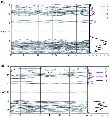 |
| | Fig. 4 Band structures of [py][BiI4] (a) and [mepy][BiI4] (b), and corresponding projected DOS (6p orbital for bismuth: purple; 5p orbital for iodine: black; 2p orbital for nitrogen: cyan; 2p orbital for carbon: magenta). The Fermi level was set at 0 eV. | |
From the computed band structure diagrams it can be seen that both [py][BiI4] and [mepy][BiI4] are semiconductors,36 with direct bandgaps of 1.8 eV (at k point (0, 0, −0.25), corresponding to the middle of k-point Y and G in Fig. 4(a)) and 2.1 eV (at k point (−0.25, 0, 0), lies halfway between k-point B(−0.5, 0, 0) and G(0, 0, 0) in Fig. 4(b)), respectively. As shown in the projected DOS (Fig. 4), the main contributor to the valence band maximum (VBM) is the iodine 5p states for both compounds. For [py][BiI4], relatively large dispersions in the band energies can be seen. In particular, high dispersions exist along vectors H–Y and G–Z, which correspond to the direction along the infinite [BiI4]− chains in real space. More interestingly, there is some small dispersion along the vector path Z–D, which corresponds to the interaction of iodine atoms between the anionic inorganic chains. Minor, but noticeable, dispersion also occurs along Y–G that arises from the short I⋯C and I⋯H contacts. For [mepy][BiI4], the valence band is generally flat. Small but noticeable dispersions along G–H and E–C in the valence band coincide with the one-dimensional chain direction. Thus, one aspect of valence band dispersion is contributed by the σ-bonding interaction of iodine 5p states with the bismuth 6p states, which leads to the infinite Bi–I covalent bonding that builds the chain structure. The other valence band interaction stemming from the iodine 5p states gives rise to the short I⋯I, I⋯C and I⋯H contacts. Therefore, dispersion in the valence band of [py][BiI4] mainly originates from the inorganic entities, and the intermolecular interaction of inter-chain iodine atoms is crucial for increasing the dispersion of the band structure. However, Louvain et al.29 claimed that due to the non-spherical distribution of the bismuth 6s orbital, it is not possible to have ideal antibonding interactions for bismuth with the surrounding six iodine atoms. This is interpreted as the imperfect geometry of the BiI6 octahedron hindering the Bi–I antibonding interactions, which leads to the relatively small band dispersion compared to lead perovskite.
As presented in Fig. 4, the conduction band minimum (CBM) for both [py][BiI4] and [mepy][BiI4] is almost entirely derived from atomic orbital contributions of nitrogen and carbon from the organic moieties. Although the overall band dispersion is not very significant, it is still worth noting that the cationic organic entities play an essential role in the CBM to increase the electronic dispersion of the band structure. Hence, participation of organic entities at band edges was found for both compounds, which may be a strategy that can be further exploited to enable higher charge transport ability in more than one dimension. Therefore, the relatively small amount of dispersion observed in the frontier orbitals of [mepy][BiI4] is derived from the lack of intermolecular interaction, which correlates with the crystal structure. However, by taking advantage of extended 1D frameworks together with the high dimensional intermolecular interactions, [py][BiI4] can be regarded as a pseudo-three-dimensional material due to its higher dimensionality in the X-ray structure and resulting band structure.
Optical and electrochemical studies
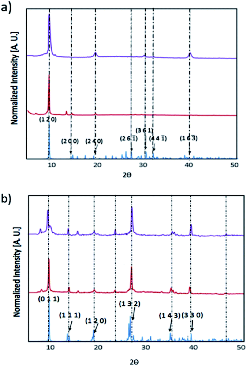
We have prepared thin films of [py][BiI4] and [mepy][BiI4] by a one-step spin-coating method (see the Experimental section). X-ray diffraction was carried out to compare with the theoretical XRD pattern of the single-crystal phase to explore the crystallinity and phase of each material in solid-state thin films (Fig. 5). Both materials as thin films are consistent with the calculated powder XRD pattern, indicating that they are predominately in the same crystallographic phase. There was no indication of the potential impurities BiI3, I2 or elemental Bi (Fig. S7†). However, strong preferred orientation on the (1 2 0) plane was observed in [py][BiI4], which corresponds to the plane where the sheet of iodobismuthate chains propagates in a parallel manner to the substrate (Fig. S3†). Preferred orientations on planes (0 1 1) and (1 3 2), along with other Bragg peaks in accordance with the simulated XRD pattern were found for [mepy][BiI4]. In addition, the stability of thin films under ambient conditions was also proven by observing XRD patterns on thin-films, which indicated that no major structural changes occurred after one-week exposure to air in the dark. Some slight improvement in crystallinity was observed over a week, possibly due to complete loss of some residual solvent in the film.
 |
| | Fig. 5 X-ray diffraction patterns for thin [py][BiI4] film (top) and thin [mepy][BiI4] film (bottom) on quartz glass slides, shown in normalized intensity versus 2θ. Simulated pattern: blue; XRD pattern for thin-films: red; XRD pattern for thin-films after one-week exposure to the air in the dark: purple. | |
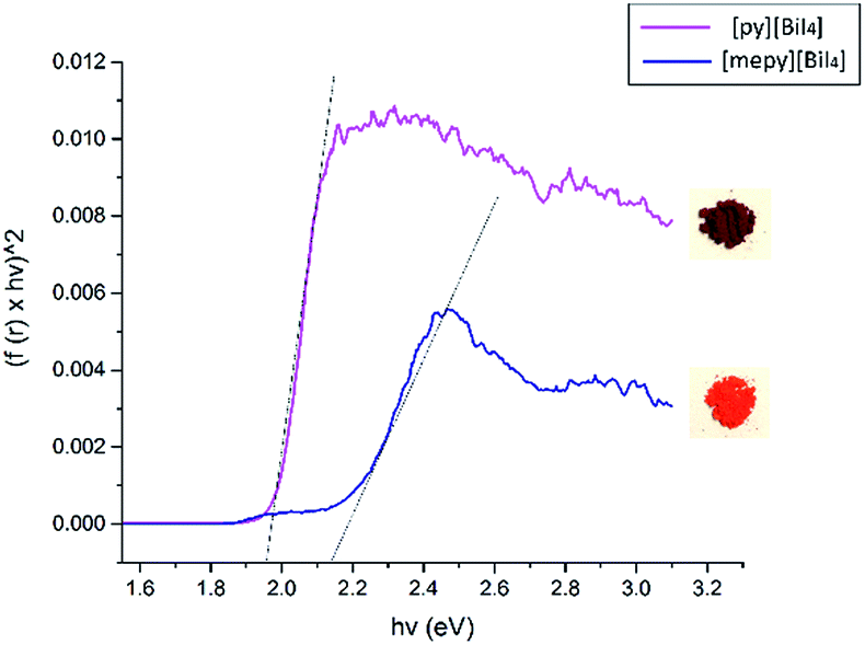
Diffuse reflectance spectra were measured for both compounds in the powder form, as well as for spin-coated samples on glass slides, in order to estimate their optical band gaps, as converted into Tauc plots. Band gap values of [py][BiI4] and [mepy][BiI4] in the powder form are 1.98 eV and 2.17 eV, respectively (Fig. 6), which compare favourably with the values obtained by simulation (DFT is well known to underestimate band gap energies).37 The observed variation in band gap for [py][BiI4] and [mepy][BiI4] is mainly caused by the differences in the organic cations present, which lead to a lack of extended inter-chain interactions for the latter compound. Slightly higher band gap values were observed for the compounds when presented as thin films (Fig. S8†), which is likely due to less-reliable measurements caused by the limited thickness of the thin film. Compared to the reported 1D (BiI4)− compounds based on metal cations30 which have band gap values of 1.70–1.76 eV, it is apparent that both 1D (BiI4)− anionic chains and the organic entities are important in determining the overall optical properties of the material.
 |
| | Fig. 6 Tauc plots and bandgap estimations for [py][BiI4] (magenta) and [mepy][BiI4] (navy), powder samples diluted in BaSO4. Photos of both powders are shown on the right side to illustrate their appearance. | |
To determine the stoichiometry of elements and probe the electronic properties of the film surface, X-ray photoelectron spectroscopy (XPS) was carried out for each compound spin-coated on fluorine-doped tin oxide (FTO) glass. The survey spectrum of each film shows that the elements detected include Bi, I, N, O, Sn and C (Fig. S9†). Both Sn and O originate from the FTO glass substrate. Fig. 7 shows the intensity of Bi 4f and I 3d core-level high-resolution photoemission for both compounds, where the binding energy is referenced to the Fermi level. The characteristic signals for Bi and I are Bi 4f7/2(158 eV), 4f5/2 (163 eV), I 3d5/2 (620 eV) and 3d3/2 (631 eV). However, some metallic bismuth was found as signals of Bi 4f7/2 (156 eV) and Bi 4f5/2 (161 eV), indicating some reduction of iodobismuthates. We speculate that this may occur during the annealing step and in future work more careful control of this step may be required. We note that the absence of diffraction peaks for elemental Bi (vide supra) suggests its presence in an amorphous or a very small particle form. The existence of metallic bismuth was also observed in the literature.14
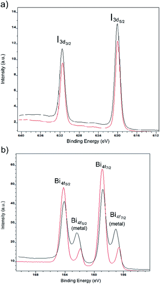 |
| | Fig. 7 Iodine 3d (a) and bismuth 4f (b) XPS spectra for thin films of [py][BiI4] (red) and [mepy][BiI4] (black). | |
To study the materials electrochemically, [py][BiI4] and [mepy][BiI4] were spin-coated on FTO conducting glass slides as working electrodes. Both of the compounds exhibited irreversible first oxidation and first reduction processes (Fig. S10†), which is likely related to some dissolution of the film after the redox step. The method from Crespilho et al.38 was used to estimate the ionization energy (IE) and the electron affinity (EA) from the experimentally determined redox potentials. The electrochemically determined IE and EA energy levels of each compound are summarized in Table 2, and the corresponding energy level diagram is shown in Fig. 8. It's worth noting that the electronically determined Eg values are consistent with the computational and optical results, which further proves the validity of the energy level measurements.
Table 2 The electrochemical oxidation onset potential (E′ox), electrochemical oxidation potential (Eox), ionization energy (IE), electronically determined energy band gap (Eg) and estimated electron affinity energy (EA) values for [py][BiI4] and [mepy][BiI4]. The relationship between the oxidation potential onset and Ag/AgCl electrode is shown in the equation Eox = E′ox + EAg/AgCl ≈ E′ox + Evac + 4.4
| Compounds |
E′ox (V vs. Ag/AgCl) |
E
ox (V vs. Ag/AgCl) |
IE (eV) |
E
g (eV) |
EA (eV) |
|
[py][BiI4]
|
0.23 |
4.63 |
−4.63 |
1.78 |
−2.85 |
|
[mepy][BiI4]
|
0.49 |
4.89 |
−4.89 |
2.38 |
−2.51 |
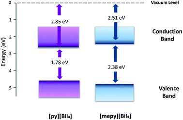 |
| | Fig. 8 Energy level diagram for [py][BiI4] and [mepy][BiI4], with Evac set at 0 eV. | |
Device characterization
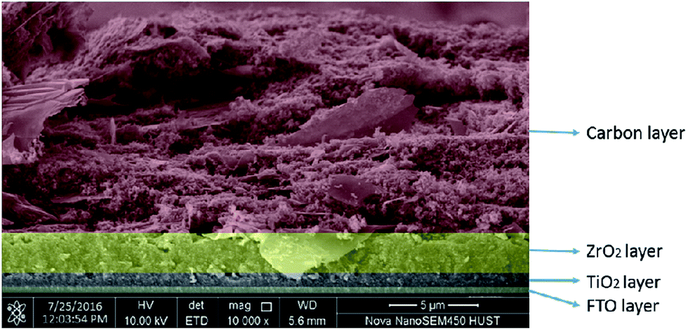
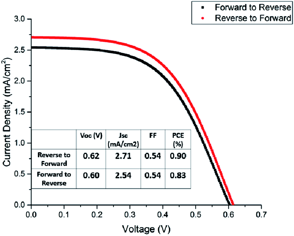
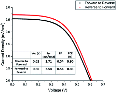
The title compounds were tried as light harvesters in solar cells. The device used in this study is based on the FTO/(TiO2/ZrO2/carbon)/perovskite structure, with the cross-section SEM image shown in Fig. 9. This type of fully printable and low-cost solar cell was first developed by H. W. Han's group.39–41 Mesoscopic TiO2, ZrO2 and carbon were printed on FTO glass layer by layer, followed by infiltrating the perovskite solution into the scaffold. No HTM was employed as was presently done in all high efficiency perovskite solar cells, so the compound transports both electrons and holes here. It was found that some [py][BiI4] starts to crystallize on the surface of the carbon film before it reaches TiO2, thus resulting in a poor reproducibility of the devices (Fig. S12†). The problem of filling can be minimized by choosing an appropriate solvent and optimizing the fabrication technique, however, it is beyond the scope of this article. Fig. 10 shows the performance of a [py][BiI4] solar cell with relatively good filling, giving a PCE of 0.90% (with Voc = 0.62 V, Jsc = 2.71 mA cm−2, FF = 0.54, reverse to forward scan). The hysteresis effect was evaluated by performing a reverse scan (from Voc to Jsc) and a forward scan (from Jsc to Voc), and substantial hysteresis has been found. In contrast, no photovoltaic effect was observed for [mepy][BiI4], which can be attributed to many reasons, e.g., poor crystallization in the mesoscopic structure, low carrier density and relatively large bandgap. For future research, it is apparent that more attention should be paid to the cationic part of the iodobismuthate complex, especially those with more electron-withdrawing and electronically delocalized properties.
 |
| | Fig. 9 Cross-sectional SEM image of the mesoscopic triple-layer solar cell architecture. | |
 |
| | Fig. 10 Boltzmann-fitted J–V curves of the [py][BiI4] champion cell. | |
Conclusion
Synthesis, structural characterization, electronic characterization and evaluation in solar cells have been carried out for two novel organic–inorganic iodobismuthate compounds, to assess their potential as third-generation lead-free photovoltaic absorbers. The crystallographic structures for both [py][BiI4] and [mepy][BiI4] feature one-dimensional [BiI4]− infinite anionic chains, while the organic entities, protonated aromatic heterocycles, play an active role in promoting intermolecular interactions and have energies close to the conduction band minimum, which supports our strategy towards enhanced pseudo-three-dimensional charge carrier transport ability. The energy levels of each compound were experimentally and computationally determined, and found to have band gaps of about 2.0 eV. Both compounds are solution-processable, which provides potential low-cost manufacturing via spin-coating methods for thin film preparation. Although some difficulty was encountered in achieving highly reproducible PV results, we demonstrated that the efficiency of the perovskite solar cell without HTM can approach 0.9%, which is comparable with the other best Bi–iodide based cells reported.17,19 This was achieved within the approach of a fully printable cell using a cell structure not explored before for iodobismuthate materials. Considering the fact that no HTM was used in the structure, this performance is very competitive. Overall, this study provides a new perspective in designing lead-free photovoltaics, by seeking to take advantage of both the anionic chain framework and the organic cation for enhanced electronic properties. Our further studies will be aimed at optimising the design of the organic cation to further promote strong intermolecular interactions.
Experimental
Materials
All the chemicals were obtained from Sigma-Aldrich and used as received, unless otherwise stated. The following chemicals were used as starting materials: bismuth(III) iodide (powder, 99%), pyridine (99.8%), iodomethane (≥99.0%), hydriodic acid (55%), water (distilled), dimethylformamide (≥99.0%), dimethylsulfoxide (≥99.0%) and ethanol (analytical grade). 1H NMR was carried out in deuterated oxide (D2O) for pyridinium iodide and 1-methylpyridinium iodide on a Bruker Advance Pro500 spectrometer and referenced externally to SiMe4.
Growth of single crystals
Single crystals of [py][BiI4] and [mepy][BiI4] were crystallized from solvent layering of ethanol solution of BiI3 and water solution of pyridinium or methylpyridinium iodide, and red plate/block-shaped crystals were formed at the interface of these two solutions by slow reaction in an NMR tube.
Film formation
Thin films of [py][BiI4] and [mepy][BiI4] were formed on glass/conducting FTO glass substrates by spin coating, using a Laurell WS-6505-6NPP-LITE spin coater. A solution of each compound was prepared by mixing equimolar organic moieties (1.0 M for pyridinium iodide, methylpyridinium iodide) and BiI3 in the same solvent (DMF![[thin space (1/6-em)]](https://www.rsc.org/images/entities/char_2009.gif) :DMSO = 7:3) and stirring at room temperature for 3 h. For spin-coating, 60 μL of solution was carefully deposited over the entire surface of a 1.5 × 1.5 cm glass/conducting FTO glass slide. The spin-coating process was performed at 2000 rpm for 1 min, or a thicker layer was made with 1000 rpm for 45 s on the glass for powder XRD measurements. In both cases, this was followed by annealing on a hot plate at 100 °C in a dry nitrogen glove box (relative humidity less than 30%, at room temperature), yielding a reddish-orange coloured film for [py][BiI4] and orange coloured film for [mepy][BiI4].
:DMSO = 7:3) and stirring at room temperature for 3 h. For spin-coating, 60 μL of solution was carefully deposited over the entire surface of a 1.5 × 1.5 cm glass/conducting FTO glass slide. The spin-coating process was performed at 2000 rpm for 1 min, or a thicker layer was made with 1000 rpm for 45 s on the glass for powder XRD measurements. In both cases, this was followed by annealing on a hot plate at 100 °C in a dry nitrogen glove box (relative humidity less than 30%, at room temperature), yielding a reddish-orange coloured film for [py][BiI4] and orange coloured film for [mepy][BiI4].
Crystal structure determination
For each compound, a suitable-sized crystal was selected and mounted on a MITIGEN holder in Paratone oil on a Rigaku Oxford Diffraction SuperNova diffractometer. The data collection was carried out at T = 120.0 K. Olex2 (ref. 42) was used when solving the structure with the ShelXS43 structure solution program. Direct methods were used for two crystals. For each compound, the model was refined with version 2014/6 of ShelXL43 using Least Squares minimisation. All non-hydrogen atoms were refined anisotropically, and positions of hydrogen atoms were calculated geometrically and refined using the riding model.
Powder XRD
X-ray diffraction on powder samples (PXRD) was recorded for the compounds over a 2θ scattering angle of 5–50 degrees. The samples were spin-coated on glass slides (see details in the Film formation section) for measurements, and monochromatic CuKα radiation with a wavelength of 1.5406 Å was used. The measurement was performed at room temperature on a Bruker D8 Advance diffractometer, with a rotation speed of 8° per min, and an increment of 0.05° on the 2θ scale.
X-ray photoelectron spectroscopy
X-ray photoelectron spectra were obtained at the National EPSRC XPS Users' Service (NEXUS) at Newcastle University. All the spectra were acquired using a Kratos Axis Nova XPS spectrometer. The samples were manipulated using clean plastic tweezers and immobilised on top of a clean aluminium plate using carbon tape. Al-Kα radiation was used as the excitation source.
Computational details
Density functional theory (DFT) based computational studies were carried out using the CASTEP 16.11 computational package34 utilizing the PBE functional44 with the TS dispersion correction scheme45 to study the electronic band structures of [py][BiI4] and [mepy][BiI4]. The initial geometry coordinates were obtained from single crystal XRD results generated from VESTA software.46 ‘On-the-fly’ pseudopotentials were generated directly from the CASTEP package, and a series of single-point energy calculations identified suitable cut-off energies for plane wave basis sets (450 eV for [py][BiI4] and 500 eV for [mepy][BiI4]), such that of dEtot/dEcut ≤ 0.003 eV per atom. Unit cell parameters were fixed at experimental values and structures were considered optimised once the standard convergence criteria were reached (maximum change in system energy 2.0 × 10⁻⁵ eV per atom, maximum force 0.05 eV Å−1, and maximum root-mean square (RMS) atomic displacement 0.002 Å). Brillouin zone sampling for each structure was achieved using Monkhorst–Pack grids such that the separation between k-points was less than 0.08 Å−1. Band structure plots were then calculated with respect to k-vectors linking high symmetry points, and also via selected k-points corresponding to strong intermolecular interactions, as indicated in Fig. S4.† Density of states (DOS) plots for each crystal structure were generated by using OptaDOS,36 which also permitted the projection to obtain the partial DOS plots, which in turn permitted the contributions from different elements to be ascertained.
UV-vis diffuse reflectance
Diffuse reflectance measurements were carried out for a spin-coated thin film and powders of each compound, on a Jasco V-670 spectrophotometer with SpectraManager software. The measurements were performed at room temperature in the range of 250–850 nm. The Kubelka–Munk function was used to analyse the data collected from diffuse reflectance measurements, and values of direct band gap of each compound were constructed using Tauc plots. The validity of assumptions on allowed direct lowest energy transitions was considered together with the result from DFT calculations.
Electrochemistry measurement
Electrochemical studies were carried out in dichloromethane, and 0.3 M N(C4H9)4PF6 was used as the supporting electrolyte. The solution was degassed with N2 for 15 minutes before each measurement. A three-electrode cell with an Autolab Type III potentiostat was used, and the results were analysed using GPES electrochemical software. The spin-coated compounds on FTO conducting glasses were used as working electrodes; Pt was used as the counter electrode; Ag/AgCl was used as the reference electrode. In the cyclic voltammetry measurement for each compound, scan rates were varied between 20 and 200 mV s−1 for every redox process, and the potential of the ferrocenium/ferrocene (Fc+/Fc) couple was used as an internal standard, taken to be at 0.63 V against NHE.
Solar cell fabrication
Two detached electrodes on FTO-coated glass were formed by laser etching, and then ultrasonically cleaned with detergent, deionised water, ethanol and UV-ozone treatment. A compact layer of TiO2 was deposited on FTO via spray pyrolysis at 450 °C from a titanium diisopropoxide bis(acetyl acetonate) solution then the screen-printing method was used to deposit a 0.4 μm mesoporous TiO2 layer, a 1.5 μm ZrO2 spacer layer, and a ∼10 μm carbon layer on the substrate. Details of slurry preparation and screen-printing parameters can be found in the literature.39 Both TiO2 and ZrO2 layers were sintered at 500 °C for 30 minutes; the carbon layer was sintered at 400 °C for 30 minutes. The same precursor solutions were used as in film formation. 4 μL precursor solution was allowed to drip from the carbon layer and penetrate into the mesoscopic triple layers. The solar cells were then heated at 40 °C overnight with a glass cover, to allow a slow crystallization process.
Photovoltaic characterization
A Keithley Model 2400 digital solar simulator with an AM 1.5G filter (model number: 91192, Oriel) was used to obtain the photocurrent density versus voltage characteristics. An irradiance of 100 mW cm−2 was used, which was calibrated using the standard reference cell (Fraunhofer ISE). The device was covered by a black mask with a circular aperture (0.07 cm2) which is smaller than the active size of the device (0.5 cm2). With a scan rate of 0.1 V s−1, both forward (short-circuit to open-circuit) and reverse (open-circuit to short-circuit) scans were applied to the device.
Acknowledgements
We thank the University of Edinburgh for financial support and access to high performance computing resources (via the ECDF), along with the EaSTCHEM Research Computing facility for access to software. We thank the National EPSRC XPS Users' Service (NEXUS) at Newcastle University for performing XPS analysis, and Dr Gary S. Nichol from the University of Edinburgh's single-crystal X-ray structure determination service for solving the crystal structures. Y. Hu and H. W. Han acknowledge financial support from the National Natural Science Foundation of China (91433203, 61474049), the Ministry of Science and Technology of China (863, 2015AA034601), and the Science and Technology Department of Hubei Province (2013BAA090). We also thank the Analytical and Testing Center of Huazhong University of Science and Technology for performing the SEM measurement.
Notes and references
- A. Kojima, K. Teshima, Y. Shirai and T. Miyasaka, J. Am. Chem. Soc., 2009, 131, 6050–6051 CrossRef CAS PubMed.
- J.-H. Im, C.-R. Lee, J.-W. Lee, S.-W. Park and N.-G. Park, Nanoscale, 2011, 3, 4088–4093 RSC.
- L. Etgar, P. Gao, Z. Xue, Q. Peng, A. K. Chandiran, B. Liu, M. K. Nazeeruddin and M. Grätzel, J. Am. Chem. Soc., 2012, 134, 17396–17399 CrossRef CAS PubMed.
- M. M. Lee, J. Teuscher, T. Miyasaka, T. N. Murakami and H. J. Snaith, Science, 2012, 338, 643–647 CrossRef CAS PubMed.
- H.-S. Kim, C.-R. Lee, J.-H. Im, K.-B. Lee, T. Moehl, A. Marchioro, S.-J. Moon, R. Humphry-Baker, J.-H. Yum, J. E. Moser, M. Grätzel and N.-G. Park, Sci. Rep., 2012, 2, 591–597 Search PubMed.
- L. Etgar, MRS Bull., 2015, 40, 674–680 CrossRef CAS.
- N. J. Jeon, J. H. Noh, W. S. Yang, Y. C. Kim, S. Ryu, J. Seo and S. I. Seok, Nature, 2015, 517, 476–480 CrossRef CAS PubMed.
- W. S. Yang, J. H. Noh, N. J. Jeon, Y. C. Kim, S. Ryu, J. Seo and S. I. Seok, Science, 2015, 348, 1234–1237 CrossRef CAS PubMed.
- M. Saliba, T. Matsui, J.-Y. Seo, K. Domanski, J.-P. Correa-Baena, K. N. Mohammad, S. M. Zakeeruddin, W. Tress, A. Abate, A. Hagfeldt and M. Gratzel, Energy Environ. Sci., 2016, 9, 1989–1997 CAS.
- M. H. Kumar, S. Dharani, W. L. Leong, P. P. Boix, R. R. Prabhakar, T. Baikie, C. Shi, H. Ding, R. Ramesh, M. Asta, M. Graetzel, S. G. Mhaisalkar and N. Mathews, Adv. Mater., 2014, 26, 7122–7127 CrossRef CAS PubMed.
- F. Hao, C. C. Stoumpos, D. H. Cao, R. P. H. Chang and M. G. Kanatzidis, Nat. Photonics, 2014, 8, 489–494 CrossRef CAS.
- N. K. Noel, S. D. Stranks, A. Abate, C. Wehrenfennig, S. Guarnera, A.-A. Haghighirad, A. Sadhanala, G. E. Eperon, S. K. Pathak, M. B. Johnston, A. Petrozza, L. M. Herz and H. J. Snaith, Energy Environ. Sci., 2014, 7, 3061–3068 CAS.
- T. Singh, A. Kulkarni, M. Ikegami and T. Miyasaka, ACS Appl. Mater. Interfaces, 2016, 8, 14542–14547 CAS.
- S. Öz, J. C. Hebig, E. Jung, T. Singh, A. Lepcha, S. Olthof, F. Jan, Y. Gao, R. German, P. H. M. van Loosdrecht, K. Meerholz, T. Kirchartz and S. Mathur, Sol. Energy Mater. Sol. Cells, 2016, 158, 195–201 CrossRef.
- R. L. Z. Hoye, R. E. Brandt, A. Osherov, V. Stevanovic, S. D. Stranks, M. W. B. Wilson, H. Kim, A. J. Akey, J. D. Perkins, R. C. Kurchin, J. R. Poindexter, E. N. Wang, M. G. Bawendi, V. Bulovic and T. Buonassisi, Chem.–Eur. J., 2016, 22, 2605–2610 CrossRef CAS PubMed.
- M. Lyu, J. H. Yun, M. Cai, Y. Jiao, P. V. Bernhardt, M. Zhang, Q. Wang, A. Du, H. Wang, G. Liu and L. Wang, Nano Res., 2016, 9, 692–702 CrossRef CAS.
- B. W. Park, B. Philippe, X. Zhang, H. Rensmo, G. Boschloo and E. M. J. Johansson, Adv. Mater., 2015, 27, 6806–6813 CrossRef CAS PubMed.
- M. B. Johansson, H. Zhu and E. M. J. Johansson, J. Phys. Chem. Lett., 2016, 7, 3467–3471 CrossRef CAS PubMed.
- Y. Kim, Z. Yang, A. Jain, O. Voznyy, G.-H. Kim, M. Liu, L. N. Quan, F. P. Garcia de Arquer, R. Comin, J. Z. Fan and E. H. Sargent, Angew. Chem., Int. Ed., 2016, 55, 9586–9590 CrossRef CAS PubMed.
- L. M. Wu, X. T. Wu and L. Chen, Coord. Chem. Rev., 2009, 253, 2787–2804 CrossRef CAS.
- M. Węcławik, A. Gągor, R. Jakubas, A. Piecha-Bisiorek, W. Medycki, J. Baran, P. Zieliński and M. Gałązka, Inorg. Chem. Front., 2016, 3, 1306 RSC.
- I. P. Aleksandrova, A. A. Sukhovsky and K. S. Aleksandrov, Solid State Commun., 1998, 105, 323–326 CrossRef CAS.
- B. Saparov, F. Hong, J.-P. Sun, H.-S. Duan, W. Meng, S. Cameron, I. G. Hill, Y. Yan and D. B. Mitzi, Inorg. Mater., 2011, 37, 623–627 Search PubMed.
- K. Eckhardt, V. Bon, J. Getzschmann, J. Grothe, F. M. Wisser and S. Kaskel, Chem. Commun., 2016, 52, 3058–3060 RSC.
- V. F. Machulin, F. V. Motsnyi, E. Y. Peresh, O. M. Smolanka and G. S. Svechnikov, Fiz. Nizk. Temp., 2004, 30, 1283–1286 Search PubMed.
- E. Y. Peresh, V. B. Lazarev, S. V. Kun, I. E. Barchii, A. V. Kun and V. I. Sidei, Mixed Halides A3B2C9 (A = Rb, Cs; B = Sb, Bi; C = Br, I) and Their Solid Solutions, Inorg. Mater., 1997, 33, 362–365 CAS.
- A. J. Lehner, D. H. Fabini, H. A. Evans, C. A. Hébert, S. R. Smock, J. Hu, H. Wang, J. W. Zwanziger, M. L. Chabinyc and R. Seshadri, Chem. Mater., 2015, 27, 7137–7148 CrossRef CAS.
- D. B. Mitzi and P. Brock, Inorg. Chem., 2001, 40, 2096–2104 CrossRef CAS PubMed.
- N. Louvain, N. Mercier and F. Boucher, Inorg. Chem., 2009, 48, 879–888 CrossRef CAS PubMed.
- N. A. Yelovik, A. V. Mironov, M. A. Bykov, A. N. Kuznetsov, A. V. Grigorieva, Z. Wei, E. V. Dikarev and A. V. Shevelkov, Inorg. Chem., 2016, 55, 4132–4140 CrossRef CAS PubMed.
- A. M. Goforth, M. D. Smith, L. Peterson and H. C. Zur Loye, Inorg. Chem., 2004, 43, 7042–7049 CrossRef CAS PubMed.
- S. V. Krivovichev and S. K. Filatov, Am. Mineral., 1999, 84, 1099–1106 CrossRef CAS.
- A. Gągor, M. Węcławik, B. Bondzior and R. Jakubas, CrystEngComm, 2015, 17, 3286–3296 RSC.
- S. J. Clark, M. D. Segall, C. J. Pickard, P. J. Hasnip, M. I. J. Probert, K. Refson and M. C. Payne, Zeitschrift für Kristallographie–Crystalline Materials, 2005, 220, 567–570 CrossRef CAS.
- A. J. Morris, R. J. Nicholls, C. J. Pickard and J. R. Yates, Comput. Phys. Commun., 2014, 185, 1477–1485 CrossRef CAS.
-
N. W. Ashcroft and N. D. Mermin, Solid State Physics, Holt-Saunders Int., 1976 Search PubMed.
- K. Burke, J. Chem. Phys., 2012, 136, 150901–150909 CrossRef PubMed.
- F. N. Crespilho, V. Zucolotto, J. R. Siqueira, A. J. F. Carvalho, F. C. Nart and O. N. Oliveira, Int. J. Electrochem. Sci., 2006, 1, 151–159 CAS.
- Z. Ku, Y. Rong, M. Xu, T. Liu and H. Han, Sci. Rep., 2013, 3, 3132–3136 Search PubMed.
- A. Mei, X. Li, L. Liu, Z. Ku, T. Liu, Y. Rong, M. Xu, M. Hu, J. Chen, Y. Yang, M. Grätzel and H. Han, Science, 2014, 345, 295–298 CrossRef CAS PubMed.
- Y. Sheng, Y. Hu, A. Mei, P. Jiang, X. Hou, M. Duan, L. Hong, Y. Guan, Y. Rong, Y. Xiong and H. Han, J. Mater. Chem. A, 2016, 4, 16731–16736 CAS.
- O. V. Dolomanov, L. J. Bourhis, R. J. Gildea, J. A. K. Howard and H. Puschmann, J. Appl. Crystallogr., 2009, 42, 339–341 CrossRef CAS.
- G. M. Sheldrick, Acta Crystallogr., Sect. A: Found. Crystallogr., 2008, 64, 112–122 CrossRef CAS PubMed.
- J. P. Perdew, K. Burke and M. Ernzerhof, Phys. Rev. Lett., 1996, 77, 3865–3868 CrossRef CAS PubMed.
- A. Tkatchenko and M. Scheffler, Phys. Rev. Lett., 2009, 102, 073005 CrossRef PubMed.
- K. Momma and F. Izumi, J. Appl. Crystallogr., 2011, 44, 1272–1276 CrossRef CAS.
Footnote |
| † Electronic supplementary information (ESI) available. CCDC 1507844–1507845 & crystallographic information, k-point path on the first Brillouin zone, illustration of intermolecular interactions, XPS survey spectrum, solar cell devices, etc. For ESI and crystallographic data in CIF or other electronic format see DOI: 10.1039/c6se00061d |
|
| This journal is © The Royal Society of Chemistry 2017 |
Click here to see how this site uses Cookies. View our privacy policy here. 
 Open Access Article
 This Open Access Article is licensed under a
  b,
Yue
Hu
*a,
Carole A.
Morrison
b,
Wenjun
Wu
b,
Hongwei
Han
a and
Neil
Robertson
b,
Yue
Hu
*a,
Carole A.
Morrison
b,
Wenjun
Wu
b,
Hongwei
Han
a and
Neil
Robertson