
Phosphorus-doped TiO2 nanotube arrays for visible-light-driven photoelectrochemical water oxidation†
Dong-Dong
Qin
 *a,
Qiu-Hong
Wang
a,
Jing
Chen
a,
Cai-Hua
He
a,
Yang
Li
a,
Cai-He
Wang
a,
Jing-Jing
Quan
a,
Chun-Lan
Tao
*b and
Xiao-Quan
Lu
*a
*a,
Qiu-Hong
Wang
a,
Jing
Chen
a,
Cai-Hua
He
a,
Yang
Li
a,
Cai-He
Wang
a,
Jing-Jing
Quan
a,
Chun-Lan
Tao
*b and
Xiao-Quan
Lu
*a
aKey Lab of Bioelectrochemistry and Environmental Analysis of Gansu, College of Chemistry and Chemical Engineering, Northwest Normal University, Lanzhou, Gansu 730070, People's Republic of China. E-mail: qindd05@gmail.com; luxq@nwnu.edu.cn
bSchool of Physical Science and Technology, Lanzhou University, Lanzhou, Gansu 730000, People's Republic of China. E-mail: taochl@lzu.edu.cn
First published on 9th January 2017
Abstract
Phosphorus-doped TiO2 nanotube arrays have been prepared via a phosphine annealing protocol and have been found to be efficient towards visible-light-driven water oxidation. Optimal visible light photocurrents of 0.25 mA cm−2 at 1.23 V and 0.85 mA cm−2 at 2.0 V vs. the RHE are achieved, which are the best reported values for phosphorus-doped TiO2.
Highly oriented titanium oxide (TiO2) nanotubes (TNTs) have been widely used as an anode material for photoelectrochemical water oxidation because of their high stability, high efficiency under UV light, and environment friendly properties and the low cost for their raw materials.1 What is more, such a one dimensional architecture offers fast charge transport and a large surface area for sufficient contact with the electrolyte.2–4 However, the total photoconversion efficiency of pristine TiO2 is limited to less than 2.2% under AM 1.5G illumination due to its low electronic conductivity and weak visible light harvesting capability.5 In this context, doping TiO2 with metal or nonmetal elements has been proposed to increase its carrier density and extend the working spectrum to the visible light region, in turn enhancing its photoconversion efficiency. For example, Sn4+,6 W6+,7 or Ta5+,8-doped TiO2 displays at least one order of magnitude increase in its carrier density. This improves the conductivity and charge separation of TiO2, thus enhancing its water oxidation performance due to increased band bending via upshifting the Fermi level towards the conduction band. Band gap narrowing by using N3− doping9 or Ti3+ self-doping10 has shown some successes in improving the visible light efficiency of TiO2. The former one is caused by mixing between N 2p and O 2p states, which lifts the valence band maximum.11 The latter is due to the formation of donor states below the conduction band.12
Recently, chemical doping by the introduction of P has been popular to tailor the electronic structure and band gap of TiO2. Compared with N3− doping, P can be incorporated into the lattice of TiO2 with two different oxidation states (P5+ or P3−) by substituting Ti4+ or O2− sites, respectively. This enables one to selectively modify the electronic properties of TiO2 by using P5+ or P3− in terms of application. A few P5+ as well as P5+ and P3− codoped TiO2 materials have been reported and demonstrated improved photocatalytic activity;13–16 however, the visible light efficiency of these materials is still far less than that of N-doped TiO2. In addition, it has been reported by some researchers that P5+ itself is unlikely to be capable of narrowing the band gap of TiO2.13 Therefore, the origin of enhanced visible light activity in P5+-doped TiO2 is still a matter of active debate although theoretical calculation has been conducted to clarify these controversial results.17 The goal of this study is to prepare highly visible light active P-doped TiO2 and to explore underlying fundamental factors responsible for enhanced performance.
In this work, P5+-doped vertically aligned TiO2 nanotube arrays are achieved by annealing in a phosphine atmosphere at a relatively low temperature (300 °C). The resulting samples are fully characterized and used to explore the fundamental factors influencing the photoelectrochemical performance as a function of doping level. The optimized sample exhibits a photocurrent of 2.8 mA cm−2 at 1.23 V vs. the RHE, as well as a visible light photocurrent of 0.25 mA cm−2 at 1.23 V and 0.85 mA cm−2 at 2.0 V vs. the RHE. The outstanding performance of P5+-doped TiO2 is found to be a consequence of improved conductivity as well as accelerated charge injection and separation. The notably increased visible light response, which is comparable to that of N-doped TiO2, can be mainly attributed to the formation of oxygen vacancies in the TiO2 structure created during phosphine annealing.
In a typical synthesis (Scheme 1), TiO2 nanotube arrays are grown using anodic oxidation in the electrolyte of 0.3 wt% NH4F and 3.0 wt% H2O in ethylene glycol, with an applied potential of 50 V and variable reaction time (3, 5, 7, 8, 10 and 15 h). Afterward, the sample is annealed in air at the temperatures ranging from 300 to 700 °C. PH3 is generated by thermal decomposition of sodium hypophosphite hydrate (NaH2PO2·H2O) at 300 °C,18 and reacts with TiO2 nanotubes at the same temperature in a tube furnace under a N2 atmosphere (Phosphine is highly toxic and the reaction should be conducted in a fume hood!). The resulting samples are used as the working electrode to set up a three-electrode photoelectrochemical system, with Pt foil as the counter electrode and a saturated calomel electrode (SCE) as the reference electrode.
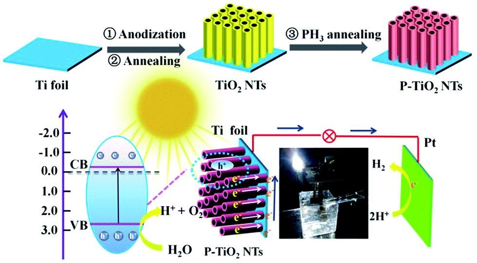 | ||
| Scheme 1 A schematic illustration showing the preparation of P-doped TiO2 nanotube arrays and the photoelectrochemical system. | ||
The SEM and TEM images of TiO2 nanotube arrays (TNTs) before and after P doping are shown in Fig. 1. It is seen that the undoped TNT is highly oriented and perpendicular to the substrate, with its pore size ranging from 138 to 150 nm, a wall thickness of 16 to 19 nm, and a length of about 17.5 μm. The doped tubes show a similar morphology and length to the undoped samples, together with an identical d-spacing of about 0.350 nm for anatase TiO2 (101) planes,19 indicating that the tubes are not damaged and the crystal polymorph is not significantly changed during doping. To further confirm this result, XRD is conducted and it is found that both doped and undoped samples exhibit one dominant and several weak peaks that can be assigned to the TiO2 anatase planes (JCPDS no. 21-1272): (101), (004), (200) (105) and (211).20 For the doped sample, the 2-theta positions of the dominant (101) as well as (200) and (211) peaks resemble those of the undoped sample. Whereas, the (004) and (105) peaks shift a little to a higher degree by 0.1° compared with that of undoped TiO2. This can be assigned to the average ionic radii difference between 6 coordinate complexes of P5+ (0.380 Å) and those of Ti4+ (0.605 Å).13 The small shifts in the 2-theta position suggest that the contractions in the unit cell caused by P5+ doping are negligible. It is noted that the TNTs with annealing temperatures above 550 °C show a weak rutile diffraction signal (Fig. S1†), coincident with the reported temperature for TiO2 phase transition from anatase to rutile.21
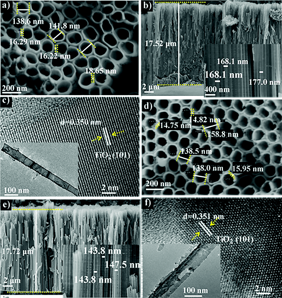 | ||
| Fig. 1 SEM images of pristine (a and b) and P-doped (d and e) TiO2 nanotube arrays. (c) and (f) are TEM images of pristine and P-doped TiO2 nanotubes, respectively. | ||
Linear X-ray mapping in Fig. 2a–d reveals the existence of P in the doped samples, indicating the successful introduction of P into TiO2 nanotubes by using PH3 annealing. The XPS analysis shown in Fig. 2e–g and S2† further demonstrates their chemical nature. In the Ti 2p XPS spectrum of undoped TiO2, two main peaks centered at 458.5 and 464.2 eV are the characteristic signals of Ti 2p3/2 and Ti 2p1/2, respectively.22 For the doped samples, the position of these two peaks shifts slightly to a higher binding energy by only 0.2 eV. This suggests that Ti3+ is not produced during doping even though PH3 is a reducing gas. The fitting curve of O 1s spectra of undoped TiO2 shows one dominant peak at 529.7 eV and a satellite peak at 531.1 eV. The former one can be ascribed to the lattice O2− and the latter is associated with the hydroxyl group or water molecules on the surface of the sample.23 In P-doped TiO2, besides the signal of lattice oxygen at 529.8 eV, two new peaks are observed with a binding energy of 530.9 and 532.7 eV, corresponding to P![[double bond, length as m-dash]](https://www.rsc.org/images/entities/char_e001.gif) O and P–O–P bonds in the phosphate.18 A single peak of the P 2p line that appeared at 133.4 eV for doped TiO2 can be attributed to P5+ in phosphate.24 Considering the limited penetration depth of XPS analysis (usually less than 5 nm) and the high reactivity of P3− with oxygen, the surface of the P-doped sample is etched by argon sputtering to check whether P3− exists in the bulk. We note that the etched sample also shows a single peak at about 134.0 eV. Hence, there is no evidence to support the existence of P3− in the doped sample since it should give rise to a signal at about 130 eV.25 From the above results, it can be concluded that P is indeed successfully incorporated into the TiO2 nanotubes but with only a singe chemical state of +5. This is different from NH3-annealed TiO2, for which N is generally introduced as N3− anions.9
O and P–O–P bonds in the phosphate.18 A single peak of the P 2p line that appeared at 133.4 eV for doped TiO2 can be attributed to P5+ in phosphate.24 Considering the limited penetration depth of XPS analysis (usually less than 5 nm) and the high reactivity of P3− with oxygen, the surface of the P-doped sample is etched by argon sputtering to check whether P3− exists in the bulk. We note that the etched sample also shows a single peak at about 134.0 eV. Hence, there is no evidence to support the existence of P3− in the doped sample since it should give rise to a signal at about 130 eV.25 From the above results, it can be concluded that P is indeed successfully incorporated into the TiO2 nanotubes but with only a singe chemical state of +5. This is different from NH3-annealed TiO2, for which N is generally introduced as N3− anions.9
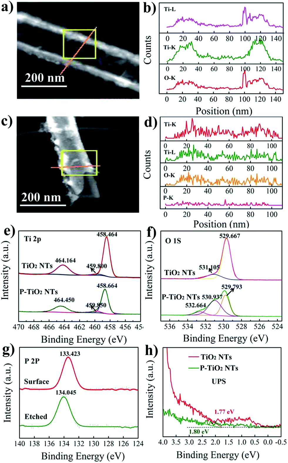 | ||
| Fig. 2 Linear X-ray mapping of pristine (a and b) and P-doped (c and d) TiO2 nanotube arrays; Ti 2p (e) and O 1s (f) XPS spectra of both pristine and P-doped TiO2 nanotube arrays, as well as P 2p XPS spectra of P-doped TiO2 nanotube arrays before and after surface etching by argon sputtering (g); UPS spectra of the samples (h). | ||
In previous studies, a blue or red shift of the absorption band edge is observed in P5+-doped TiO2. These ambivalent results have long been a debate and have not been completely clarified to date. Compared with P-containing organic precursors, PH3 is a cleaner P source and would not introduce other impurities. Thus, the valance band of P5+-doped TiO2 synthesized in this work is investigated by UPS (ultraviolet photoelectron spectroscopy) to gain insight into the effect of P5+ doping on the band structure. In the UPS spectra, the intercepts on the energy axis characterize the valance band energy with respect to the Fermi level. As can be seen in Fig. 2h, the valance band maxima for pristine and doped TiO2 are determined to be about 1.77 and 1.80 eV, respectively. The comparable value indicates that the valance band is not changed following the doping. Besides, P5+ is unlikely to be capable of downward shifting the conduction band minimum since the defect states induced by cations with oxidation states higher than +4 are located above the conduction band minimum of TiO2.26 These results show that the band structure of TiO2 nanotubes is not evidently influenced by doping, excluding the possibility of P5+ doping for narrowing the band gap. The previously observed visible light response of P5+-doped TiO2 (ref. 27–29) may be caused by other effects which accompanies the doping process.
The photoelectrochemical performance of the samples is evaluated under AM 1.5G (100 mW cm−2) illumination in 1.0 M NaOH. Fig. 3a and S3† show the photocurrent of 500 °C annealed TNTs with different anodization times, obtained at 1.23 V vs. the RHE. We note that the 7 h TNTs display the best photocurrent of 1.0 mA cm−2. An anodization time shorter or longer than that leads to a decrease of the photocurrent, probably due to the balance between the light penetration depth and electron diffusion length. Although high temperature annealing can be helpful to completely remove the organic residue and improve the crystallinity of TNTs, it may cause, we think, difficulty for the diffusion of P into the lattice of TiO2.30 On the basis of this understanding, the 7 h TNTs are optimized by annealing in air at variable temperature (from 300 to 700 °C). Subsequently, these samples are annealed in PH3 (generated by using 1.0 g NaH2PO2·H2O) at 300 °C to produce P5+-doped TNTs. As shown in Fig. 3b, S4 and S5,† the doped samples exhibit enhanced photocurrent within the entire temperature window relative to the undoped TNTs. The optimal photocurrent of about 2.5 mA cm−2 is achieved from P5+-doped 500 °C annealed 7 h TNTs. This result reveals that effective P5+ doping, at least in our study, highly relies on the crystallinity of the TiO2 precursor. The low crystalline TiO2 may facilitate the diffusion of doping ions, thus achieving a higher doping level, but low conductivity and a high recombination rate would be deleterious to getting a high photocurrent. When using high temperature (>500 °C) annealed TNTs as the doping precursor, the decreased photocurrent of P5+-doped TiO2 is evidently observed and may be explained by three reasons: (1) insufficient doping due to the high crystallinity of precursor TiO2; (2) phase transition from anatase to rutile, leading to interior photoactivity; (3) increased thickness of the oxide layer underlying the TNTs.
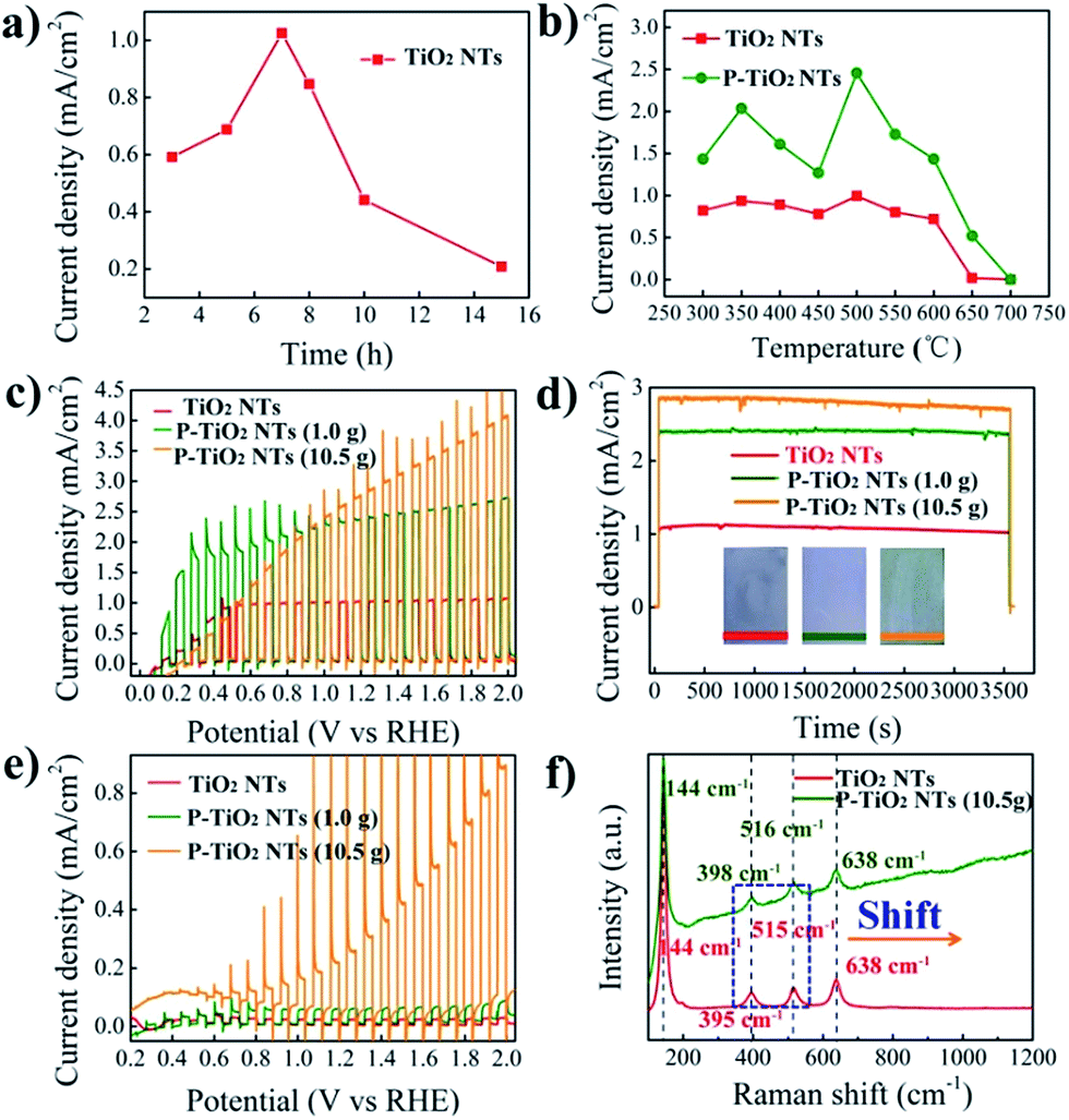 | ||
| Fig. 3 (a) Photocurrent of 500 °C annealed TiO2 nanotube arrays with different anodization times, as well as (b) photocurrent of 7 h TiO2 nanotube arrays with different annealing temperatures and that after PH3 annealing at 300 °C, recorded at 1.23 V vs. the RHE; (c) photocurrent of pristine and P-doped 500 °C annealed 7 h TiO2 nanotube arrays, and (d) corresponding long-term stability measurements under full light illumination (insets are the photographs of the samples); (e) photocurrent of pristine and P-doped 500 °C annealed 7 h TiO2 nanotube arrays under visible light; (f) Raman spectra of pristine and P-doped 500 °C 7 h annealed TiO2 nanotube arrays. | ||
To investigate the effect of the doping level on the performance of the samples, we have explored a higher concentration of PH3 by increasing the amount of NaH2PO2·H2O to 10.5 g. As can be seen in Fig. 3c, a further enhanced photocurrent of about 2.8 mA cm−2 at 1.23 V vs. the RHE is obtained, corresponding to a peak solar energy conversion efficiency of 1.1% (Fig. S6†). This photocurrent is among the highest values reported, such as those of cross-linked TiO2 nanowires (2.5 mA cm−2 at 1.23 V vs. the RHE),31 as well as hydrogenated-TiO2 (2.5 mA cm−2 at 0.23 V vs. Ag/AgCl)32 and Sn-doped TiO2 nanorods (2.0 mA cm−2 at 0 V vs. Ag/AgCl).6 Continuously increasing the concentration of PH3 or doping temperature (>300 °C) would not elevate the photocurrent. The long-term stability measurements shown in Fig. 3d indicate the high stability of the P5+-doped TNTs as a photoanode. This implies that P5+ can stably exist in TiO2 and is unlikely to be reduced to lower oxidation states by photogenerated electrons during photoelectrochemical reactions.
The visible light photoresponse is measured under chopped light illumination (>420 nm) and demonstrated in Fig. 3e. It can be seen that the undoped TNTs show a negligible photocurrent owing to their large band gap (3.2 eV). A slightly enhanced photocurrent of 50 μA cm−2 at 1.23 V vs. the RHE for the P5+-doped TNTs is obtained when using a low concentration of PH3 (1.0 g NaH2PO2·H2O). Surprisingly, largely increased photocurrents of 0.25 at 1.23 V vs. the RHE and 0.85 mA cm−2 before the onset of dark current are achieved at a high concentration of PH3 (10.5 g NaH2PO2·H2O). It is not uncommon that a high concentration of phosphorous source yields a high doping level of P5+, therefore notably enhancing the performance. The visible light photocurrent of 0.25 mA cm−2 at 1.23 V vs. the RHE is comparable to those of N3−-doped TiO2 nanorods with NH3 (ref. 33) or NH3–H2 (ref. 34) annealing, as well as S2−-doped TNTs with H2S annealing.35 Yet, it is still lower than that of N3−-doped TiO2 nanorods prepared by ion implantation.36 Note that P5+ is unable to modify the valance band position of TiO2, as evidenced by UPS measurements. We postulate that the visible light response may be caused by oxygen vacancies in the TiO2 structure created during PH3 annealing. This defect state has been found in the hydrogen or ammonia treated TiO2, with the energy level below the conduction band of pristine TiO2.33 As a result, transition from the TiO2 valance band to oxygen vacancy levels may lead to visible light responses (Fig. S7†). To check the existence of oxygen vacancies in P-doped TiO2, Raman spectra are acquired and shown in Fig. 3f and S8.† The four characteristic Raman peaks at 144, 395, 515 and 638 cm−1 in undoped TiO2 can be assigned to Eg, B1g, A1g and Eg modes of the anatase phase, respectively.37 Compared with undoped TiO2, the frequency of B1g and A1g modes in the P-doped sample shows blue shifts by 3 and 1 cm−1, respectively, being indicative of an increased concentration of oxygen vacancies, thus supporting our hypothesis.38
In order to further understand the enhanced photoelectrochemical performance of P5+-doped TiO2, electrochemical impedance spectroscopy (EIS) is conducted under illumination and the results are shown in Fig. 4a. The smaller semicircle of the doped sample in the Nyquist plots reveals superior charge transfer at the TiO2–electrolyte interface. This result is then supported by the improved charge injection efficiency evaluated by using H2O2 as the hole scavenger as shown in Fig. 4b, S9 and S10.† Additionally, we note from Fig. 4c that the charge separation efficiency in the bulk of the electrode is also largely enhanced after doping. To explain this phenomenon, Mott–Schottky plots are made and displayed in Fig. 4d. The positive slope of doped TiO2 indicates n-type electronic conduction features,39 consistent with the observed anodic photocurrent. Furthermore, as compared with undoped TiO2, the substantially smaller slope of the doped sample implies a higher concentration of carriers. Through analysis of the Mott–Schottky plots, a three order of magnitude increase in the carrier density, from 5.92× 1019 cm−3 for undoped to 2.33 × 1022 cm−3 for doped TiO2, is indeed observed. The increased carrier density may be attributed to the P5+ dopant and introduced oxygen vacancies, both of which are reported to be electron donors for TiO2.13,40 Following the increase of the carrier density, the conductivity of TiO2 can be undoubtedly improved. Meanwhile, the band bending would increase as well by upshifting the Fermi level and reducing the thickness of the depletion layer. Thus, the charge separation is accelerated.
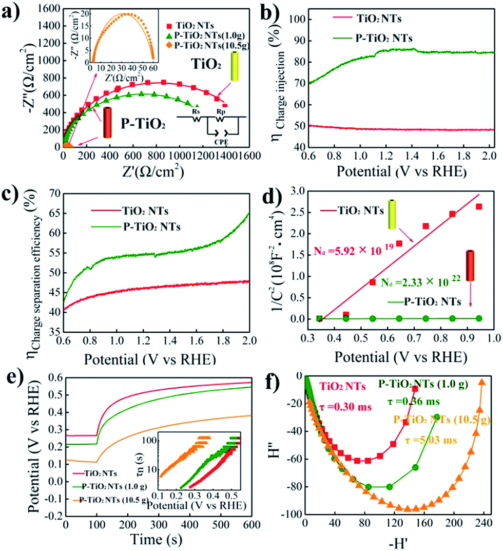 | ||
| Fig. 4 Electrochemical impedance spectra (EIS) (a), charge injection (b) and separation (c) efficiencies, Mott–Schottky plots (d), open circuit voltage (Voc) decay (e) and intensity modulated photocurrent spectroscopy (IMPS) (f) of the pristine and P-doped TiO2 nanotube arrays with different doping levels. | ||
The electron recombination kinetics of the samples are monitored by using open circuit voltage (Voc) decay. As seen in Fig. 4e, the positive decay of the open circuit voltage further confirms the n-type semiconductor characteristic of P5+-doped TiO2.41 Importantly, heavily P5+-doped TiO2 (10.5 g NaH2PO2·H2O) shows the lowest Voc decay rate among the samples tested, implying the longest lifetime of photogenerated electrons. To confirm this, the average lifetime of electrons is estimated by conversion of Voc decay using the methodology developed by Bisquert et al.42 We see in the inset that the electron lifetime of heavily P5+-doped TiO2 is apparently longer than that of undoped as well as lightly doped TiO2, consistent with the lowest Voc decay rate. In general, a longer electron lifetime should enhance the performance of the photoanode since the prolonged lifetime increases the probability for the photoexcited carriers to be used for photochemical reactions.43,44
Finally, intensity modulated photocurrent spectroscopy (IMPS) is employed to investigate the charge transport properties of the samples.45 The average lifetime for photoexcited electrons to diffuse to an electrode can be estimated by the equation of τD= (2πfIMPs)−1, where τD is the transit time and fIMPs is the frequency at which the minimum in the IMPS plot occurs. As illustrated in Fig. 4f, the heavily P5+-doped TiO2 shows a relatively longer transport time of 5.03 ms, as compared with 0.30 and 0.36 ms for undoped and lightly doped TiO2, respectively. Broadly speaking, a longer transport time may increase the possibility of charge recombination and, hence, decrease the photoelectrochemical performance. Yet, the highest photocurrent observed in the heavily doped sample demonstrates the efficient electron transport.46 Another possibility for a longer transport time in the samples with a higher photocurrent is that, we assume, a high electron concentration in semiconductors may increase the repulsion effect between electrons and thus lead to delayed travel of electrons to the electrode. It is possible that although more time is needed for electron transport to the electrode, the number of electrons collected in the electrode could be high. As a result, a high photocurrent is obtained.47
Conclusions
Doping TiO2 with impurity elements has been a classical approach to extend the working spectrum of TiO2 to the visible light region for application in photoelectrochemical devices. However, for nonmetal doping, this concept mainly focuses on N3− and S2−. We have demonstrated that P5+ doping via PH3 annealing can greatly improve the photoelectrochemical performance of TiO2 nanotube photoanodes and achieve an outstanding visible photocurrent. The heavily doped TiO2 without cocatalyst modification yields a visible photocurrent of 0.25 mA cm−2 at 1.23 V and 0.85 mA cm−2 at 2.0 V vs. the RHE, which are the best reported values for P-doped TiO2 to date. The enhanced performance can be mainly ascribed to the oxygen vacancies as well as improved charge injection and separation efficiencies. Due to the reducing ability of PH3 and variable chemical states of P, the PH3 annealing strategy may be extended to other semiconductors for improving visible light photoactivity via multi-doping effects.Acknowledgements
This work is supported financially by the National Natural Science Foundation of China for Young Scholars (No. 21401150 and 21501083), the National Natural Science Foundation of China (No. 51562034, 21327005, and 21575115), the Gansu Province Science Foundation for Distinguished Young Scientist (No. 1606RJDA315) and the Program for Chang Jiang Scholars and Innovative Research Team, Ministry of Education of China (No. IRT1283).Notes and references
- J. Schneider, M. Matsuoka, M. Takeuchi, J. L. Zhang, Y. Horiuchi, M. Anpo and D. W. Bahnemann, Chem. Rev., 2014, 114, 9346 CrossRef PubMed.
- X. D. Wang, Z. D. Li, J. Shi and Y. H. Yu, Chem. Rev., 2014, 114, 9346 CrossRef CAS PubMed.
- B. Liu and E. S. Aydil, J. Am. Chem. Soc., 2009, 131, 3985 CrossRef CAS PubMed.
- X. J. Feng, K. Zhu, A. J. Frank, C. A. Grimes and T. E. Mallouk, Angew. Chem., Int. Ed., 2012, 124, 2781 CrossRef.
- S. Hoang, S. P. Berglund, N. T. Hahn, A. J. Bard and C. B. Mullins, J. Am. Chem. Soc., 2012, 134, 3659 CrossRef CAS PubMed.
- M. Xu, P. M. Da, H. Y. Wu, D. Y. Zhao and G. F. Zheng, Nano Lett., 2012, 12, 1503 CrossRef CAS PubMed.
- Z. F. Tong, T. Peng, W. W. Sun, W. Liu, S. S. Guo and X. Z. Zhao, J. Phys. Chem. C, 2014, 118, 16892 CAS.
- X. J. Feng, K. Shankar, M. Paulose and C. A. Grimes, Angew. Chem., Int. Ed., 2009, 121, 8239 CrossRef.
- C. Blackman, C. J. Carmalt, I. P. Parkin and S. O'Neill, Chem. Mater., 2002, 14, 3167 CrossRef CAS.
- F. Zuo, L. Wang, T. Wu, Z. Y. Zhang, D. Borchardt and P. Y. Feng, J. Am. Chem. Soc., 2010, 132, 11856 CrossRef CAS PubMed.
- X. B. Chen, L. Liu, P. Y. Yu and S. S. Mao, Science, 2011, 331, 746 CrossRef CAS PubMed.
- Y. Q. Gai, J. B. Li, S. S. Li, J. B. Xia and S. H. Wei, Phys. Rev. Lett., 2009, 102, 036402 CrossRef PubMed.
- C. Sotelo-Vazquez, N. Noor, A. Kafizas, R. Quesada-Cabrera, D. O. Scanlon, A. Taylor, J. R. Durrant and I. P. Parkin, Chem. Mater., 2015, 27, 3234 CrossRef CAS.
- D. D. Qin, X. H. Wang, Y. Li, J. Gu, X. M. Ning, J. Chen, X. Q. Lu and C. L. Tao, J. Phys. Chem. C, 2016, 120, 22195 CAS.
- S. A. Ansari and M. H. Cho, Sci. Rep., 2016, 6, 25405 CrossRef CAS PubMed.
- Y. H. Peng, J. F. He, Q. H. Liu, Z. H. Sun, W. S. Yan, Z. Y. Pan, S. Z. Liang, W. R. Cheng and S. Q. Wei, J. Phys. Chem. C, 2011, 115, 8184 CAS.
- R. Long and N. J. English, ChemPhysChem, 2011, 12, 2604 CrossRef CAS PubMed.
- Z. F. Hu, Z. R. Shen and J. C. Yu, Chem. Mater., 2016, 28, 564 CrossRef CAS.
- J. G. Yu, J. J. Fan and K. L. Lv, Nanoscale, 2010, 2, 2144 RSC.
- A. Razzaq, C. A. Grimes and S. I. In, Carbon, 2016, 98, 537 CrossRef CAS.
- J. Li, Z. Q. Wang, J. Wang and T. K. Sham, J. Phys. Chem. C, 2016, 120, 22079 CAS.
- T. K. Sham and M. S. Lazarus, Chem. Phys. Lett., 1979, 68, 426 CrossRef CAS.
- A. Fujishima, X. T. Zhang and D. A. Tryk, Surf. Sci. Rep., 2008, 63, 515 CrossRef CAS.
- Y. B. Wang, Y. S. Wang, R. R. Jiang and R. Xu, Ind. Eng. Chem. Res., 2012, 51, 9945 CrossRef CAS.
- C. Sotelo-Vazquez, N. Noor, A. Kafizas, R. Quesada-Cabrera, D. O. Scanlon, A. Taylor, J. R. Durrant and I. P. Parkin, Chem. Mater., 2015, 27, 3234 CrossRef CAS.
- D. S. Bhachu, S. J. Y. Sathasivam, G. Sankar, D. O. Scanlon, G. Cibin, C. J. Carmalt, I. P. Parkin, G. W. Watson, S. M. Bawaked, A. Y. Obaid, S. Al-Thabaiti and S. N. Basahel, Adv. Funct. Mater., 2014, 24, 5075 CrossRef CAS.
- O. G. Neeruganti, H. L. Hsin, F. K. Tzu, C. H. Lee, C. C. Chang, J. D. Wu, C. S. Shiann and C. K. Shyue, J. Phys. Chem. C, 2012, 116, 16191 Search PubMed.
- Y. Z. Ren, L. Li, L. X. Jing, X. Z. Yue and C. X. You, J. Phys. Chem. C, 2008, 112, 15502 Search PubMed.
- K. D. Wang, J. Yu, L. J. Liu, L. Hou and F. Y. Jin, Ceram. Int., 2016, 42, 16405 CrossRef CAS.
- D. D. Qin, C. L. Tao, S. I. In, Z. Y. Yang, T. E. Mallouk, N. Z. Bao and C. A. Grimes, Energy Fuels, 2011, 25, 5257 CrossRef.
- M. Z. Liu, N. D. L. Snapp and H. K. Park, Chem. Sci., 2011, 2, 80 RSC.
- G. M. Wang, H. Y. Wang, Y. C. Ling, Y. C. Tang, X. Y. Yang, R. C. Fitzmorris, C. C. Wang, J. Z. Zhang and Y. Li, Nano Lett., 2011, 11, 3026 CrossRef CAS PubMed.
- W. J. Yuan, J. C. Li, L. K. Wang, P. Chen, A. J. Xie and Y. H. Shen, ACS Appl. Mater. Interfaces, 2014, 6, 21978 CAS.
- S. Hoang, S. P. Berglund, N. T. Hahn, A. J. Bard and C. B. Mullins, J. Am. Chem. Soc., 2012, 134, 3659 CrossRef CAS PubMed.
- S. W. Shin, J. Y. Lee, K.-S. Ahn, S. H. Kang and J. H. Kim, J. Phys. Chem. C, 2015, 119, 13375 CAS.
- G. M. Wang, X. H. Xiao, W. Q. Li, Z. Y. Lin, Z. P. Zhao, C. Chen, C. Wang, Y. J. Li, X. Q. Huang, L. Miao, C. Z. Jiang, Y. Huang and X. F. Duan, Nano Lett., 2015, 15, 4692 CrossRef CAS PubMed.
- X. L. Tong, P. Yang, Y. W. Wang, Y. Qin and X. Y. Guo, Nanoscale, 2014, 6, 6692 RSC.
- H. L. Cui, W. Zhao, C. Y. Yang, H. Yin, T. Q. Lin, Y. F. Shan, Y. Xie, H. Gua and F. Q. Huang, J. Mater. Chem. A, 2014, 2, 8612 CAS.
- R. O'Hayre, M. Nanu, J. Schoonman and A. Goossens, J. Phys. Chem. C, 2007, 111, 4809 Search PubMed.
- A. Janotti, J. B. Varley, P. Rinke, N. Umezawa, G. Kresse and C. G. V. Walle, Phys. Rev. B: Condens. Matter Mater. Phys., 2010, 81, 085212 CrossRef.
- Y. J. Lin, Y. Xu, M. T. Mayer, Z. I. Simpson, G. McMahon, S. Zhou and D. W. Wang, J. Am. Chem. Soc., 2012, 134, 5508 CrossRef CAS PubMed.
- A. Zaban, M. Greenshtein and J. Bisquert, ChemPhysChem, 2003, 4, 859 CrossRef CAS PubMed.
- J. S. D. Chene, B. C. Sweeny, A. C. J. Peck, D. Su, E. A. Stach and W. D. Wei, Angew. Chem., Int. Ed., 2014, 53, 7887 CrossRef PubMed.
- M. K. Wang, J. Bai, F. L. Formal, S. J. Moon, L. C. Ha, R. H. Baker, C. Grätzel, S. M. Zakeeruddin and M. Grätzel, J. Phys. Chem. C, 2012, 116, 3266 CAS.
- D. Vaccarello, J. Hedges, A. Tapley, D. A. Love and Z. F. Ding, J. Electroanal. Chem., 2015, 738, 35 CrossRef CAS.
- J. Z. Su, L. J. Guo, N. Z. Bao and C. A. Grimes, Nano Lett., 2011, 11, 1928 CrossRef CAS PubMed.
- D. D. Qin, Y. Li, X. M. Ning, Q. H. Wang, C. H. He, J. J. Quan, J. Chen, Y. T. Li, X. Q. Lu and C. L. Tao, Dalton Trans., 2016, 45, 16221 RSC.
Footnote |
| † Electronic supplementary information (ESI) available: Experimental procedures, characterization, equipment, photocurrent response, XRD, XPS wide spectra, conversion efficiencies, optical spectra and Raman spectra. See DOI: 10.1039/c6se00045b |
| This journal is © The Royal Society of Chemistry 2017 |