
Scalably synthesized environmentally benign, aqueous-based binary nanoparticle inks for Cu2ZnSn(S,Se)4 photovoltaic cells achieving over 9% efficiency†
Ki-Joong
Kim
abef,
Changqing
Pan
ab,
Shalu
Bansal
 c,
Rajiv
Malhotra
c,
Dae-Hwan
Kim
d and
Chih-Hung
Chang
*ab
c,
Rajiv
Malhotra
c,
Dae-Hwan
Kim
d and
Chih-Hung
Chang
*ab
aSchool of Chemical, Biological & Environmental Engineering, Oregon State University, Corvallis, Oregon 97331, USA. E-mail: chih-hung.chang@oregonstate.edu
bOregon Process Innovation Center, Advanced Technology and Manufacturing Institute, Corvallis, Oregon 97330, USA
cDepartment of Mechanical Engineering, Oregon State University, Corvallis, Oregon 97331, USA
dConvergence Research Center for Solar Energy, Daegu Gyeongbuk Institute of Science & Technology (DGIST), Daegu 42988, South Korea
eNational Energy Technology Laboratory (NETL), U.S. Department of Energy, 626 Cochrans Mill Road, Pittsburgh, Pennsylvania 15236, USA
fAECOM, P.O. Box 618, South Park, Pennsylvania 15216, USA
First published on 4th January 2017
Abstract
Low-cost materials, scalable manufacturing, and high power conversion efficiency are critical enablers for large-scale applications of photovoltaic (PV) cells. Cu2ZnSn(S,Se)4 (CZTSSe) has emerged as a promising PV material due to its low-cost earth-abundant nature and the low toxicity of its constituents. We present a compact and environmentally friendly route for preparing metal sulfide (metals are Cu, Zn, and Sn) nanoparticles (NPs) and optimize their annealing conditions to obtain uniform carbon-free CZTSSe thin films with large grain sizes. Further, the solution-stable binary NP inks synthesized in an aqueous solution with additives are shown to inhibit the formation of secondary phases during annealing. A laboratory-scale PV cell with a Al/AZO/ZnO/CdS/CZTSSe/Mo-glass structure is fabricated without anti-reflective coatings, and a 9.08% efficiency under AM1.5G illumination is demonstrated for the first time. The developed scalable, energy-efficient, and environmentally sustainable NP synthesis approach can enable integration of NP synthesis with emerging large-area deposition and annealing methods for scalable fabrication of CZTSSe PV cells.
Introduction
The development and large-scale commercial applications of photovoltaic (PV) cells have attracted worldwide attention due to increasing energy consumption and a rising need for renewable energy sources. As a result, there are ongoing efforts towards the development of scalable PV manufacturing methods.1,2 The development of scalable and sustainable methods for the synthesis of low-cost PV materials is a necessary component of scalable PV manufacturing, in order to achieve the targeted terawatt-scale adoption of solar energy. Thin-film chalcogenide-based PV cells offer the benefits of an absorber with a direct energy band gap, facile band gap tuning, reduced sensitivity to recombination at grain boundaries, and the possibility of depositing on flexible substrates.3–5 In particular, the kesterite Cu2ZnSn(S,Se)4 (CZTSSe) is regarded as a promising photovoltaic (PV) material due to the earth-abundant and low toxicity nature of its constituents.6The most efficient CZTSSe thin film PV cell to date, prepared by a hydrazine-based solution process, has demonstrated a device efficiency of over 12%.7,8 However, the high toxicity and potentially explosive nature of hydrazine limit the scalability of this approach.9 An alternative route is to employ solution-based nanoparticles (NPs). Achieving a promising PV efficiency with quaternary CZTS NPs10–17 is difficult due to the limited control of the bulk composition of the thin film. An alternative NP-based approach is selenization (i.e., annealing in the presence of selenium) of binary or ternary metal sulfide NPs, such as Cu2SnS3, Cu2−xS, ZnS, and SnSx, in different stoichiometric ratios.18,19 These NPs are typically synthesized by the hot-injection technique, which is well suited to the production of small amounts of NPs in a batch reactor (typically a few tens of milligrams) but has insufficient yield for most practical applications. Microfluidic flow reactors have been developed for continuous NP production,20–22 and can potentially produce a higher NP yield per unit spatial volume of equipment than larger batch reactors within a relatively smaller volume. However, most work on such reactors has focused on controlling NP properties and the potential for scalable NP synthesis has not been fully exploited.
Another common issue with the NP-based approach is the residual carbon produced in selenization, due to the long organic chains used to chemically bond the as-synthesized NPs.15,18,19 This carbon blocks crystallization and produces multi-layered structures with both large-grain and small-grain layers. This phenomenon significantly deteriorates the film's electronic properties, e.g. resulting in a high series resistance.10,11,23 To improve the device performance by reducing the series resistance and enhancing the absorption of long wavelength photons, it is desirable to eliminate these small-grain layers. It is worth noting that starting with binary NPs which transition through an intermediate liquid phase provides a pathway for rapid mass transport during selenization, which favours the formation of large crystals through Oswald ripening.24–26 This approach assists grain growth at low temperatures and is adopted here.
Here we report a 9.08% power conversion efficiency (PCE) CZTSSe thin-film PV cell fabricated via a precursor mixture of binary NPs, prepared at room temperature in a high-throughput continuous microreactor system (Fig. 1A). Briefly, binary NPs were synthesized by continuously pumping metal precursors and the reducing agent dissolved in water into a micro-mixer at room temperature. A gas–liquid segmented flow system was used by introducing air in order to prevent clogging inside the microchannels of the micromixer. Enabled by the facileness of this continuous aqueous route and the compactness of micromixers, a high NP yield was obtained by simply using multiple micromixers in parallel, e.g., each binary NP was obtained at a rate of over ∼320 g h−1. This ability to increase the NP yield with a relatively smaller increase in the equipment size, as compared to batch reactors, has the potential for direct integration of micromixer-based NP synthesis with large-area NP deposition (e.g., roll-to-roll printing) and annealing methods (e.g., photonic and plasma annealing) without compromising on the speed of the process chain. 5 g of CZTS is needed to fabricate 1 m2 of CZTS thin film solar cells based on a rough estimation. Our three continuous-flow reactors (CuS, SnS and ZnS) combined (i.e. unit) could produce ∼1000 g h−1. Thus, one NP production unit could potentially support a 200 m2 h−1 cell manufacturing throughput. In addition, our reactors could simply be scaled up to match higher cell production throughputs by the combination of channel-up and number-up approaches.
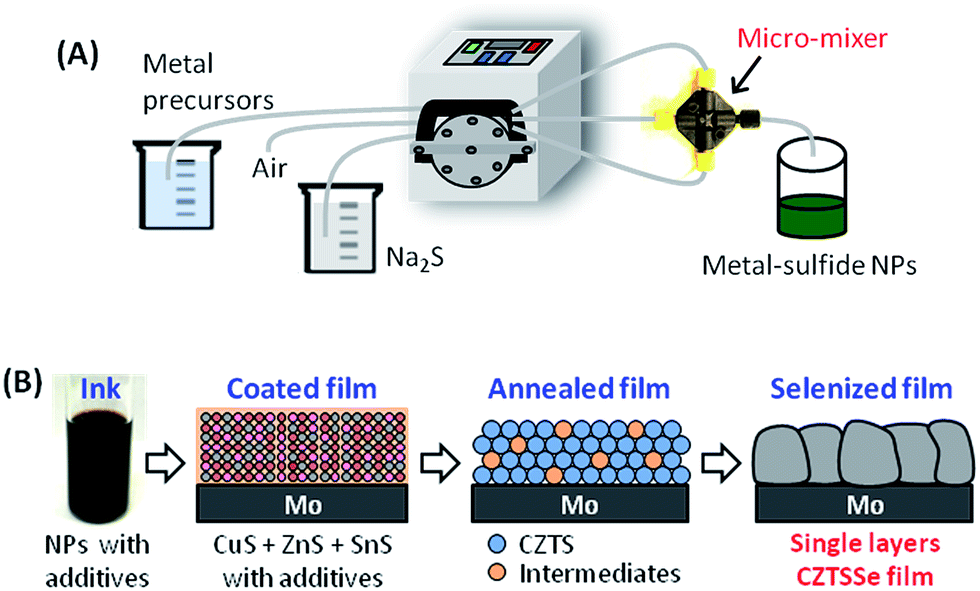 | ||
| Fig. 1 (A) Schematic diagram of the continuous flow precipitation system designed in this study for synthesizing binary NPs in aqueous solution. (B) Schematic process for large crystalline single layer CZTSSe film preparation using a solution stable binary NP-based ink. | ||
The as-prepared binary NPs were easily aggregated and precipitated due to their poor protection, leading to an unstable solution (Fig. S1 and S2, ESI†). Organic additives including monoethanolamine (MEA) and/or polyvinylpyrrolidone (PVP) were therefore introduced into the precursor solution to create a stable NP solution from the as-synthesized binary NPs. Further, MEA27–29 and/or PVP30 also reduce carbon in the absorber layer and mitigate the residual carbon induced retardation of crystallization mentioned above. The Cu/(Zn + Sn) and Zn/Sn ratios in the precursor ink were targeted at a Cu-poor and Zn-rich stoichiometry (Cu/(Zn + Sn) = 0.85 and Zn/Sn = 1.15) and were determined via elemental analysis (Fig. S3, ESI†). The solutions of binary NPs were mixed with PVP, MEA, and thiourea (TU) in 2-methoxyethanol to form the ink precursor (see the Experimental section in the ESI†). Transmission electron microscopy (TEM) and atomic resolution high-angle annular dark-field (HAADF)-scanning TEM (STEM) analyses show a homogeneous distribution of the four elements Cu, Zn, Sn and S (Fig. S4, ESI†). These precursor inks were spin-coated onto Mo/glass substrates and pre-annealed in air, followed by selenization, to form CZTSSe films (Fig. 1B). The process variables such as the additives, pre-annealing temperature, selenization temperature and time were optimized to obtain single-layer, crystalline, and carbon-free CZTSSe thin films with large grains. This CZTSSe thin film was used to fabricate a PV device consisting of Al/AZO/ZnO/CdS/CZTSSe/Mo-glass, and the device performance was characterized.
Results and discussion
We investigated the effect of additives on the formation of CZTSSe thin films. Defects, small grains, and poor adhesion were observed in pure binary NP solution without additives (Fig. S8A, ESI†). When combined with only pure MEA or pure PVP in a solution of binary NPs, the CZTSSe layer was comprised of highly crystalline large grain (top) and sparsely packed small grain layers (bottom) that are rich in carbon (Fig. S5B and C, ESI†), and thus reduce the PCE (Fig. S6, ESI†). The effect of spin-coating/annealing cycles without MEA and with MEA on the formation of CZTSSe films was also examined. Without MEA (Fig. S7, ESI†), CZTSSe films exhibited more densely packed small-grain layers and the thickness of the precursor layer increased proportionally to the number of spin-coating/annealing cycles. Initial attempts to increase the large grain layer using a thicker precursor layer resulted in a similar thickness of large grains on the top layer. At the same time, a thicker small grain layer was formed and it remains unchanged in spite of longer selenization times. Poor adhesion of CZTSSe layer was observed with increasing the MEA content over 0.7 mL in a solution of binary NPs (Fig. S8, ESI†). The MEA content has apparently influenced the formation of CZTSSe films; small grain bottom layers gradually decrease as the MEA content increases. Carbon-free CZTSSe films were obtained (Fig. S5D, ESI†) by combining MEA and PVP; however this approach results in porous CZTSSe layers, which can be optimized by controlling the selenization conditions (see Fig. 3).Organics such as binders and/or surfactants need to be removed from the precursor films before selenization via pre-annealing in air, to prevent the formation of a residual carbon-rich layer. However, common metal sulfide NPs easily react during pre-annealing resulting in oxygen inclusion into the final film. Therefore, the pre-annealing temperature must be suitably set to achieve carbon-free precursor films without too much oxidation. We examined the effect of pre-annealing temperatures in the range of 250–400 °C in air on the formation of precursor films (e.g. CZTS). Elemental analysis showed that Cu, Zn and Sn contents in the pre-annealed films remained fairly constant when compared to those in the precursor ink. However, there was a slight loss in S due to the formation of metal oxides. To reduce the oxidation of binary metal sulfide NPs at high temperatures, TU was added into the precursor ink as an additional sulfur source to act as a reducing agent. XRD patterns of pre-annealed precursor films showed kesterite CZTS (JCPDS 26-0575) as the majority phase, and minimal phases of metal oxides/sulfides (CuO, SnO2, SnS, and SnS2) at high pre-annealing temperatures (Fig. 2A). The peaks of SnS2 and SnO2 became more dominant, and the CuO phase disappeared at 400 °C. Note that the formation of intermediate phases, related to the Cu, Zn or S-containing compounds e.g. Cu2−xS, ZnS, Cu2SnS3 or even the ZnO phase, was not detected under all reaction conditions in the XRD patterns. For reference, Fig. 2C shows the XRD patterns of each binary NP type synthesized by a continuous flow precipitation method. However, it should be noted that the characteristic peaks of the Cu2SnS3 and the ZnS phase in the XRD pattern overlap with that of the pure CZTS phase,30 and therefore Raman analysis was utilized to assist with the phase identification of the precursor film annealed at 350 °C in air (Fig. 2E). The formation of CZTS was confirmed by the presence of peaks at 288, 338, and 368 cm−1.31 The Raman data also showed the characteristic peaks of the intermediates such as SnS (220 cm−1),32 CuO (295 cm−1),33 SnS2 (315 cm−1),32 Cu3SnS4 (or ZnS, 350 cm−1),34 SnO2 (438 and 601 cm−1),35 and Cu2−xS (473 cm−1).36 This result indicates the formation of CZTS together with Cu3SnS4 (or ZnS) and metal oxides as minor phases and is in good agreement with the XRD result. Therefore, we deduce that with increasing pre-annealing temperature a small amount of binary NPs react through the following oxidation reactions: (1) 2Cu2−xS + 3O2 → 2Cu2−xO + 2SO2 and (2) 2SnS + O2 → SnS2 + SnO2. The chemical conversion of SnS under heating in air is thermodynamically favorable because the enthalpy of formation of SnS is −100 kJ mol−1, while that of SnS2 and SnO2 is −167 kJ mol−1 and −581 kJ mol−1, respectively. Therefore, the SnS2 component persists and the SnO2 component becomes more dominant with an increase in the pre-annealing temperature in air. In addition, a MoS2 phase was formed at 400 °C by reaction with TU in the precursor ink. Thus, the pre-annealing temperature in air should be lower than 400 °C because MoS2 layers may reduce the ohmic contact between CZTSSe and Mo.37
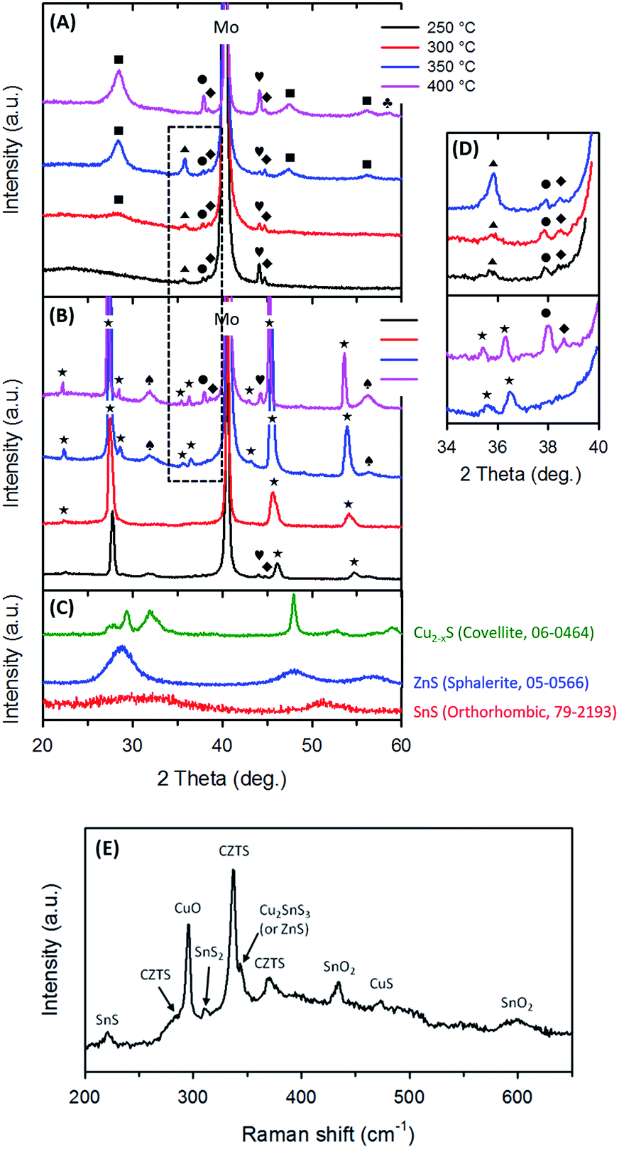 | ||
| Fig. 2 XRD patterns of (A) the pre-annealed precursor films in air and (B) the CZTSSe films after selenization at 530 °C for 30 min as a function of pre-annealing temperatures in air. (C) XRD patterns of binary NPs synthesized by a continuous flow precipitation method. (D) Enlarged XRD patterns of the pre- and the post-selenized precursor films indicated by the dotted square line in (A) and (B). Peaks are marked with (■) for CZTS, (●) for SnO2, (◆) for SnS, (▲) for CuO, (♥) for SnS2, (★) for CZTSSe, (♣) for MoS2 and (♠) for Mo(S,Se)2. (E) Raman spectrum of the precursor film annealed at 350 °C in air. | ||
Furthermore, metal oxides and tin sulfides in the precursor film pre-annealed at 350 °C in air disappeared after selenization (Fig. 2B and D) without forming any intermediates, suggesting the successful intercalation of Se ions to form CZTSSe films. CZTSSe films on Mo/glass substrates show a kesterite structure (JCPDF 52-0868) with sharpened peaks, indicating a large degree of growth in the crystal grain size and potential for high-quality PV cells. No Se-containing intermediates such as CuSe, ZnSe and SnSe2 were observed in any of the tested samples, suggesting that the formation of intermediates might be bypassed and the solid reaction pathway is fairly simple. In contrast, CZTSSe films from the precursor film pre-annealed at 400 °C in air still contained SnO2 and SnS2 components, which remained even when more aggressive selenization conditions were used. This high temperature led to an increased Mo(S,Se)2 layer (Fig. S9, ESI†). In addition to this, a poor grain growth of CZTSSe films with weak adhesion was obtained at pre-annealing temperatures below 300 °C in air (Fig. S10, ESI†). Therefore, the precursor films pre-annealed at 350 °C in air were subjected to further investigation on the formation of CZTSSe films after selenization.
Typically, device performance improves as the grain size of CZTSSe layers increases and the thickness of the Mo(S,Se)2 layers reduces,37 both being controlled by selenization conditions. The surface topography and cross-sectional scanning electron microscope (SEM) images of the CZTSSe films selenized at different temperatures and times are shown in Fig. 3. It is obvious that the precursor film pre-annealed at 350 °C in air formed a densely packed uniform layer via consecutive spin-coating. The size of grains gradually increased as the temperature increased; however, heating above 580 °C led to stress-induced cracks. The samples selenized at relatively low temperatures (500 °C and 530 °C) and at short times (10 min and 20 min) exhibited a typical bilayer structure formed by a bottom layer with small grains and a top layer with large grains, along with holes in the film. The films formed at 550 °C for 30 min produced dense, crack-free and pinhole-free single CZTSSe layers (∼1.6 μm) with micrometer-sized grains. Both the XRD and Raman data confirmed that no major crystalline secondary phases were generated under our optimized selenization conditions, at 550 °C for 30 min (Fig. 4). The composition of the CZTSSe films was Cu1.80Zn1.13Sn1(S,Se)4.13, with the concentration ratios of Cu/(Zn + Sn) = 0.85, Zn/Sn = 1.13, and Se/(S + Se) = 0.85. The ratios of Cu/(Zn + Sn) and Zn/Sn in all the CZTSSe samples are almost the same independent of selenization temperatures and times (Fig. S11, ESI†). It was also found that a longer selenization time (50 min) resulted in a higher % Se (96%) in CZTSSe films (Fig. S12, ESI†).
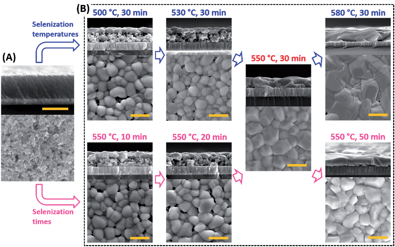 | ||
| Fig. 3 Top and cross-sectional SEM images of the (A) precursor film pre-annealed at 350 °C in air and (B) CZTSSe films selenized at different temperatures (500–580 °C) and times (10–50 min). Scale bar is 2 μm. | ||
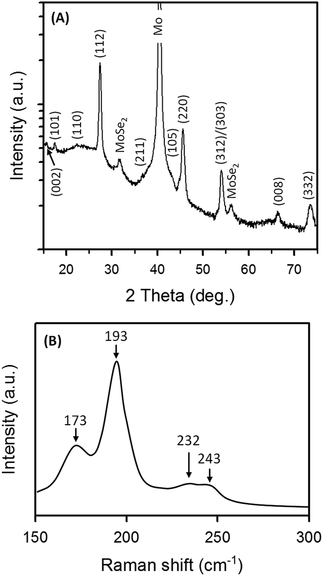 | ||
| Fig. 4 (A) Logarithmic XRD pattern and (B) Raman spectrum of the optimized CZTSSe film selenized at 550 °C for 30 min. CZTSSe film on a Mo/glass substrate can be identified as kesterite Cu2ZnSnSe4 (JCPDF 52-0868) with the tetragonal lattice constants a = b = 5.6930 Å and c = 11.3330 Å. Peaks arising from the Mo substrate and the Mo(S,Se)2 interlayer are also noted. The main peaks at 173, 193, and 232 cm−1 in the Raman spectrum confirms that CZTSe is the major phase in the sample. The peak at 243 cm−1 is possibly due to the known Mo(S,Se)2.38 In addition, within the resolution of the Raman measurement, no noticeable peaks corresponding to Cu2Se, ZnSe or Cu2SnSe3 were observed,39 which excludes the existence of possible impurity phases after selenization. | ||
The CZTSSe PV device consisted of Al/AZO/ZnO/CdS/CZTSSe/Mo-glass (see fabrication details in the Experimental section). Cross-sectional SEM images of the device showed dense, uniform films (Fig. 5A). There were also few voids at the CZTSSe/Mo(S,Se)2 interface, which could increase the series resistance. These voids could be effectively prevented by rapid heating in the selenization process.40,41 Atomic resolution HAADF-STEM, energy dispersive X-ray spectroscopy (EDS) line scanning (Fig. 5B) and mappings prepared by using a focused ion beam (FIB) (Fig. 6) confirmed the compositional uniformity of Cu, Zn, Sn, S, and Se, and a single layer CZTSSe film. The CdS buffer layer (∼50 nm) was visible in the S map as well. A slight amount of S was observed in the bulk CZTSSe film, indicating the replacement of S by Se during selenization of the precursor film. Trace amounts of Sn were detected in the Mo(S,Se)2 layer, indicating that the Sn was diffused into the Mo(S,Se)2 layer; however, no evidence was found for the presence of Sn(S,Se)x phases within the detection limit of Raman and XRD (Fig. 4). One hypothesis behind this observation is that the reaction of Sn(S,Se)x phases with Mo is thermodynamically favorable,42 yielding Sn–Mo(S,Se)2. This could be the dominant reaction because it is consistent with the no observation of Cu2−x(S,Se) and/or Zn(S,Se) phases. A 210 nm thick Mo(S,Se)2 layer was formed at the interface of the CZTSSe layer during selenization at 550 °C for 30 min. Detailed EDS compositional profiling across the CZTSSe film thickness also indicated uniform and almost identical ∼30 nm thick atomic % Cu rich layers at both the top and bottom of the CZTSSe film (Fig. S13 and S14, ESI†). While this might be thought to cause secondary phase formation such as Cu2−x(S,Se) which can reduce the performance of the PV cell, the absence of S and/or Se elements suggests a pure Cu layer.43 The X-ray photoelectron spectroscopy (XPS) depth profiles of the CZTSSe PV cell confirmed that Cu is in fact not present at the interface of the CZTSSe layer (Fig. S15, ESI†). Therefore, Cu-rich layers are an artifact caused by Cu migration from CZTSSe produced during the FIB machining.44
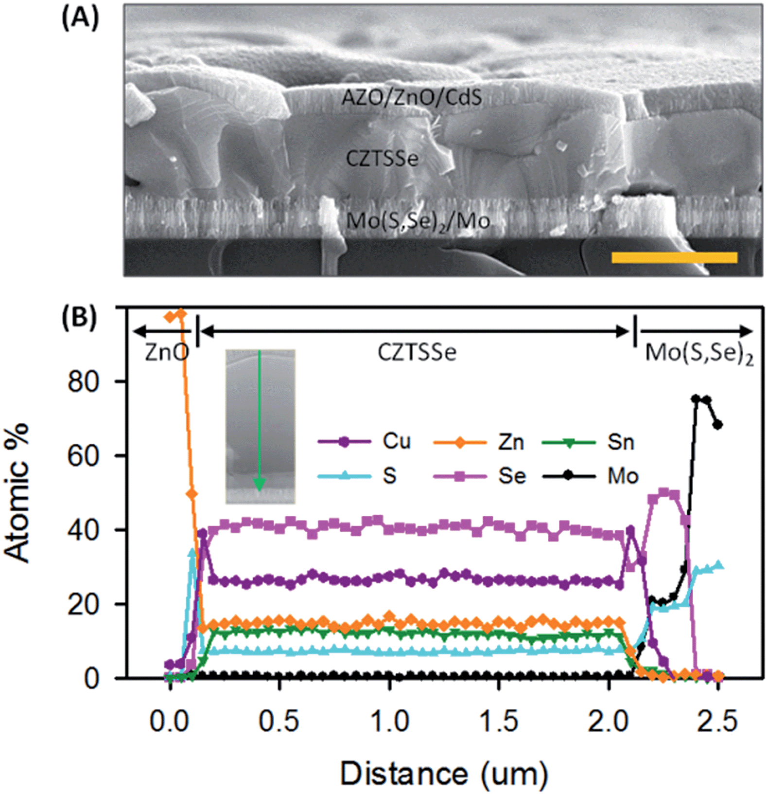 | ||
| Fig. 5 (A) Cross-sectional SEM image of the completed PV device from the CZTSSe film selenized at 550 °C for 30 min, and chemical bath deposition of CdS, sputtering of ZnO and AZO, and evaporation of Al top contacts (scale bar is 2 μm). (B) Elemental distributions (Cu, Zn, Sn, Zn, and Se) determined by EDS line scanning from the arrow in (B) (inset of the HAADF-STEM image). | ||
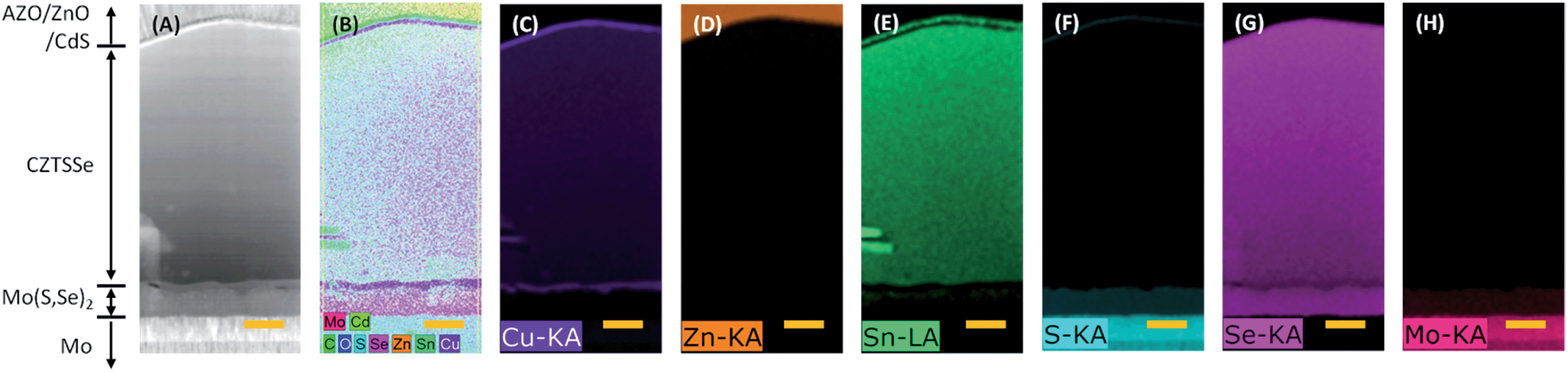 | ||
| Fig. 6 (A) Cross-sectional HAADF-STEM image of the integrated film (AZO/ZnO/CdS/CZTSSe/Mo(S,Se)2/Mo) milled by a FIB technique and (B–H) EDS mappings for the compositional distribution of the CZTSSe film. Note that S element in Mo layer (Fig. 6F) is not reliable due to emission of S spectrum overlap with Mo element. Scale bar is 300 nm. | ||
Fig. 7A shows the current–voltage (I–V) characteristics of the fabricated PV device. The device exhibited a PCE of over 9% with an open-circuit voltage (VOC) of 447.8 mV, a short-circuit current density (JSC) of 31.5 mA cm−2, and a fill factor (FF) of 0.644 (an active area of 0.09 cm2) under AM1.5 illumination, representing the highest performance efficiency (9.08% PCE) reported to date for NP-based CZTSSe PV cells without an anti-reflective coating. A small difference in JSC between EQE measurements (32.7 mA cm−2) and I–V data (31.5 mA cm−2) was observed. This is attributed to the shadowing induced by the Al top contact, which covers about 3.1% of the unit cell surface. The device showed an external quantum efficiency up to 93% and yielded an estimated CZTSSe band gap of 1.06 eV (Fig. 7B and S16, ESI†). Since the band gap for pure CZTSe and CZTS is commonly reported to be 1.0 and 1.5 eV,45 respectively, this indicates 84% of the Se content in the CZTSSe film after selenization, which is in good agreement with the XRD result (Fig. S12, ESI†). A possible cause for low VOC values compared to those of the record CZTSSe PV cells with a PCE of over 12% (ref. 7 and 8) may be the presence of SnS2 in the Mo(S,Se)2 layer, leading to an increase in the series resistance of the device because of its high band gap (2.2–2.4 eV).46 The effect of this on the contact resistance is not understood at the present time, but it may depend on how the Fermi levels of Sn–Mo(S,Se)2 line up at the junction. There are several factors that affect the PV performance related to the absorber-back contact interface: (1) the partial delamination of the absorber on the Mo substrate does lower the contact area which increases the series resistance, (2) the delamination further creates small grain-size crystals at the interface which increase the chance of carrier recombination, and the device behaves with a low shunt resistance, and (3) voids above the Mo layer could locally increase during selenization which harms the ohmic contact at the interface. The reason for the slightly low JSC value is either a fairly thick AZO window layer (∼435 nm), which partially absorbs incident light, or Al2O3 formation at the interface between the Al top contact and AZO window layer. Therefore, future work will improve the JSC and lower the series resistance of the CZTSSe device.
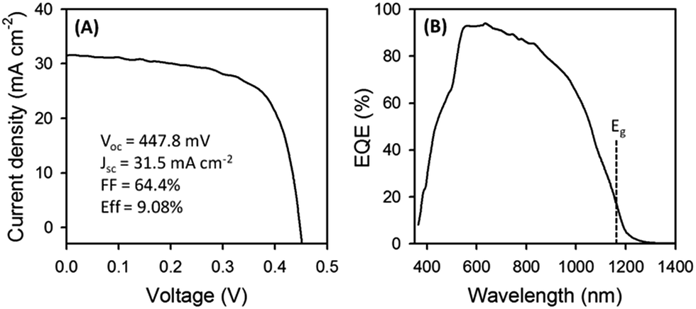 | ||
Fig. 7 (A) The current–voltage (I–V) characteristics under AM1.5 illumination and (B) external quantum efficiency curve of the 9.08% CZTSSe PV device. The dashed line in (B) marks the band gap estimated using [hν![[thin space (1/6-em)]](https://www.rsc.org/images/entities/char_2009.gif) ln(1 − EQE)]2versus the photon energy (eV) (Fig. S16, ESI†). ln(1 − EQE)]2versus the photon energy (eV) (Fig. S16, ESI†). | ||
Experimental
Materials
ACS grade copper acetate (Cu(OAc)2), zinc acetate (Zn(OAc)2), tin chloride (SnCl2), sodium sulphide, selenium powder, and monoethanolamine (MEA) were purchased from Sigma Aldrich. Polyvinylpyrrolidone (PVP, MW = 8000) from TCI America, 2-methoxyethanol (2-MTE) from Fisher Scientific, and thiourea (TU) and cadmium sulfate (CdSO4) from Alfa Aesar were bought. Double distilled water was used for the synthesis of binary NPs. All chemicals were used as purchased without further purification.Synthesis of binary NPs and ink preparation
We started the synthesis of binary CuS, ZnS, and SnS NPs, and then mixed them with PVP and MEA in 2-MTE to form ink precursors. Each binary NP type was synthesized by a simple continuous flow precipitation method without using organic surfactants as shown in Fig. 1A. In a typical synthesis, each precursor, Cu(OAc)2 (500 mmol) in 1000 mL-H2O, or Zn(OAc)2 (500 mmol) in 1000 mL-H2O, or SnCl2 (500 mmol) in 1000 mL-H2O (50 mL-HCl was added to the precursor solution of SnCl2) was mixed with Na2S (500 mmol) in 1000 mL-H2O in a micro-cross mixer (0.5 mm ID) at room temperature. PTFE tubing (0.79 mm ID) was utilized for the system resulting in a residence time below one second. A gas–liquid segmented flow system was also generated by introducing air in order to prevent the clogging problem inside the channel in a micro-cross mixer. Each flow rate was maintained at 35 mL min−1. The reaction product was collected, centrifuged, and then washed with H2O and ethanol several times. The final product was kept in EtOH or dried under vacuum at 70 °C for 12 h for further characterization.The Cu/(Zn + Sn) and Zn/Sn ratios in the precursor ink were targeted at a Cu-poor and Zn-rich stoichiometry (Cu/(Zn + Sn) = 0.85 and Zn/Sn = 1.15), as determined by the EDS analysis (Fig. S3, ESI†). Each of the three NP types were mixed with TU, MEA, and PVP in 4 mL of 2-MTE solution and then ultra-sonicated for 30 min to form a well-dispersed precursor ink, followed by another 12 h of stirring at room temperature, and then 0.5 mL of MEA was added and stirred.
CZTSSe thin film PV fabrication
Binary NP based ink was deposited on a Mo-coated glass substrate by spin coating. The samples were then pre-annealed at 250–400 °C for 1 minute in air on a hot plate. The deposition, spin coating, and annealing procedures were repeated to yield desired thickness. Next, the selenization process was performed in a quartz tube furnace with a N2 flow at 500–580 °C (ramping rate of 20 °C min−1) for 15–60 minutes. After selenization, a CdS buffer layer was coated by chemical bath deposition on the sample. Then, i-ZnO and Al doped n-ZnO window layers were deposited by RF magnetron sputtering on top of the CdS layer. Al top contacts were deposited as a current collector using a thermal evaporator. The finished devices were mechanically scribed into 3 mm by 3 mm small cells for efficiency measurements.Characterization
Crystalline phases were identified by using a X-ray diffractometer (XRD) (D8 Discover, Bruker) operating at 40 kV and a current of 40 mA with Cu Kα1 radiation (0.154 nm). The Raman spectrum was recorded using a WITec confocal Raman microscope at a 532.4 nm wavelength and with a CCD detector. X-ray photoelectron spectroscopy (XPS, ESCALAB 250, Thermo-Scientific) was performed with a monochromatized Al Kα (1486.6 eV) X-ray source. Scanning electron microscope (SEM) analysis was conducted with an FEI Quanta 600 and FEI Nova NanoSEM 230, using 5–10 kV accelerating voltage. High resolution transmission electron microscopy (HR-TEM) images and atomic resolution high-angle annular dark-field (HAADF) scanning TEM (STEM) images were obtained using an FEI Titan 80–300 operating at 300 kV. Cross sections of the sample were prepared by a focused ion beam (FIB) technique on a FEI Helios 650 dual beam SEM. TEM and STEM-EDS were carried out on an XFEG Titan TEM equipped with 4 Bruker SDDs, and a Gatan Tridiem energy filter. The PV device performance was measured using an Oriel 96000 Full spectrum solar simulator calibrated with a standard Si solar cell, a Newport radiant power meter and a PVIV-200 test station. The quantum efficiency was measured by using a Tau Science FlashQE system.Conclusions
In summary, low-cost and earth-abundant metal sulphide NPs were synthesized in an aqueous solution at room temperature via a precipitation method implemented in a compact micromixer. Solution-stable NP inks were created, and their annealing conditions were optimized, to obtain carbon-free CZTSSe films with a single layer consisting of large-crystal domains. These CZTSSe films were used to fabricate PV cells that showed the highest performance efficiency (∼9.08%) reported to date for NP-based CZTSSe PV cells without an anti-reflective coating. The compactness and high throughput (upto 320 g h−1 for each binary NP) of this micromixer-based approach can enable an increased NP yield per unit spatial volume than is typically possible with larger batch reactors, since a number of micromixers can be used in parallel within a relatively smaller spatial volume. This creates the potential for direct integration of this micromixer-based NP synthesis approach with methods for large-area NP deposition such as roll-to-roll printing, and methods for large-area NP annealing such as photonic and plasma annealing, without compromising on the speed of the entire process chain. The key to additional improvements in the device performance is further reduction of the VOC deficit. Further investigations of PV device fabrication through modifying the precursor components and optimizing the thickness of the window layer should lead to a significant increase in the efficiency using NP inks.Acknowledgements
This work was supported by the DGIST R&D Programs of the Ministry of Science, ICT & Future Planning of Korea (16-BD-05) and by the National Science Foundation grant number CMMI#1537196 and Scalable Nanomanufacturing program under Grant No. CBET-1449383. This work was also performed at the Oregon Process Innovation Center (OPIC) for Sustainable Solar Cell Manufacturing, an Oregon BEST signature research facility. We would like to thank Peter Eschbach, Guoheng Ma, and Yujuan He for their valuable assistance in obtaining and analyzing data for experimental assistance. Special thanks to McKenzie Kimball for his valuable comments and suggestions.Notes and references
- B. W. Lavery, S. Kumari, H. Konermann, G. L. Draper, J. Spurgeon and T. Druffel, ACS Appl. Mater. Interfaces, 2016, 8, 8419–8426 CAS.
- N. Rajamanickam, S. Kumari, V. K. Vendra, B. W. Lavery, J. Spurgeon, T. Druffel and M. K. Sunkara, Nanotechnology, 2016, 13, 235404 CrossRef PubMed.
- M. Kumar, A. Dubey, N. Adhikari, S. Venkatesan and Q. Qiao, Energy Environ. Sci., 2015, 8, 3134–3159 CAS.
- H. Azimi, Y. Hou and C. J. Brabec, Energy Environ. Sci., 2014, 7, 1829–1849 CAS.
- A. Polizzotti, I. L. Repins, R. Noufi, S.-H. Wei and D. B. Mitzi, Energy Environ. Sci., 2013, 6, 3171–3182 CAS.
- S. Das, K. C. Mandal and R. N. Bhattacharya, in Semiconductor Materials for Solar Photovoltaic Cells, Springer Series in Materials Science, ed. M. P. Paranthaman, W. Wong-Ng and R. N. Bhattacharya, Springer International Publishing, Switzerland, 2016, vol. 218, pp. 25–74 Search PubMed.
- W. Wang, M. T. Winkler, O. Gunawan, T. Gokmen, T. K. Todorov, Y. Zhu and D. B. Mitzi, Adv. Energy Mater., 2014, 4, 1301465 CrossRef.
- J. Kim, H. Hiroi, T. K. Todorov, O. Gunawan, M. Kuwahara, T. Gokmen, D. Nair, M. Hopstaken, B. Shin, Y. S. Lee, W. Wang, H. Sugimoto and D. B. Mitzi, Adv. Mater., 2014, 26, 7427–7431 CrossRef CAS PubMed.
- H. Zhou, W.-C. Hsu, H.-S. Duan, B. Bob, W. Yang, T.-B. Song, C.-J. Hsu and Y. Yang, Energy Environ. Sci., 2013, 6, 2822–2838 CAS.
- C. Steinhagen, M. G. Panthani, V. Akhavan, B. Goodfellow, B. Koo and B. A. Korgel, J. Am. Chem. Soc., 2009, 131, 12554–12555 CrossRef CAS PubMed.
- Q. Guo, H. W. Hillhouse and R. Agrawal, J. Am. Chem. Soc., 2009, 131, 11672–11673 CrossRef CAS PubMed.
- Q. Guo, G. M. Ford, W.-C. Yang, B. C. Walker, E. A. Stach, H. W. Hillhouse and R. Agrawal, J. Am. Chem. Soc., 2010, 132, 17384–17386 CrossRef CAS PubMed.
- A. Carrete, A. Shavel, X. Fontané, J. Montserrat, J. Fan, M. Ibáñez, E. Saucedo, A. Pérez-Rodríguez and A. Cabot, J. Am. Chem. Soc., 2013, 135, 15982–15985 CrossRef CAS PubMed.
- J. van Embden, A. S. R. Chesman, E. D. Gaspera, N. W. Duffy, S. E. Watkins and J. J. Jasieniak, J. Am. Chem. Soc., 2014, 136, 5237–5240 CrossRef CAS PubMed.
- W.-C. Hsu, H. Zhou, S. Luo, T.-B. Song, Y.-T. Hsieh, H.-S. Duan, S. Ye, W. Yang, C.-J. Hsu, C. Jiang, B. Bob and Y. Yang, ACS Nano, 2014, 8, 9164–9172 CrossRef CAS PubMed.
- J. Zhong, Z. Xia, C. Zhang, B. Li, X. Liu, Y.-B. Cheng and J. Tang, Chem. Mater., 2014, 26, 3573–3578 CrossRef CAS.
- C. K. Miskin, W.-C. Yang, C. J. Hages, N. J. Carter, C. S. Joglekar, E. A. Stach and R. Agrawal, Prog. Photovolt: Res. Appl., 2015, 23, 654–659 CrossRef CAS.
- Y. Cao, M. S. Denny, J. V. Caspar, W. E. Farneth, Q. Guo, A. S. Ionkin, L. K. Johnson, M. Lu, I. Malajovich, D. Radu, D. Rosenfeld, K. R. Choudhury and W. Wu, J. Am. Chem. Soc., 2012, 134, 15644–15647 CrossRef CAS PubMed.
- X. Lin, J. Kavalakkatt, A. Ennaoui and M. C. Lux-Steiner, Sol. Energy Mater. Sol. Cells, 2015, 132, 221–229 CrossRef CAS.
- A. M. Nightingale and J. C. de Mello, J. Mater. Chem., 2010, 20, 8454–8463 RSC.
- S. Marre and K. F. Jensen, Chem. Soc. Rev., 2010, 39, 1183–1202 RSC.
- Y. Song, J. Hormes and C. S. S. R. Kumar, Small, 2008, 4, 698–711 CrossRef CAS PubMed.
- R. Mainz, B. C. Walker, S. S. Schmidt, O. Zander, A. Weber, H. Rodriguez-Alvarez, J. Just, M. Klaus, R. Agrawal and T. Unold, Phys. Chem. Chem. Phys., 2013, 15, 18281–18289 RSC.
- C. H. Chang, B. J. Stabbery, A. Morrone, A. Davydov and T. J. Anderson, MRS Symp. Proc., 1997, 485, 163–168 CrossRef.
- B. J. Stanbery, A. Davydov, C. H. Chang and T. J. Anderson, AIP Conf. Proc., 1997, 394, 579–588 CrossRef CAS.
- B. J. Stanbery, C.-H. Chang and T. J. Anderson, Inst. Phys. Conf. Ser., 1998, 152, 915–922 CAS.
- W. Wang, Y.-W. Su and C.-H. Chang, Sol. Energy Mater. Sol. Cells, 2011, 95, 2616–2620 CrossRef CAS.
- G. M. Ilari, C. M. Fella, C. Ziegler, A. R. Uhl, Y. E. Romanyuk and A. N. Tiwari, Sol. Energy Mater. Sol. Cells, 2012, 104, 125–130 CrossRef CAS.
- Z. Su, K. Sun, Z. Han, H. Cui, F. Liu, Y. Lai, J. Li, X. Hao, Y. Liu and M. A. Green, J. Mater. Chem. A, 2014, 2, 500–509 CAS.
- K. Kim, I. Kim, Y. Oh, D. Lee, K. Woo, S. Jeong and J. Moon, Green Chem., 2014, 16, 4323–4332 RSC.
- J. Ge, J. Jiang, P. Yang, C. Peng, Z. Huang, S. Zuo, L. Yang and J. Chu, Sol. Energy Mater. Sol. Cells, 2014, 125, 20–26 CrossRef CAS.
- Y. Jayasree, U. Chalapathi and V. Sundara Raja, Thin Solid Films, 2013, 537, 149–155 CrossRef CAS.
- F. A. Akgul, G. Akgul, N. Yildirim, H. E. Unalan and R. Turan, Mater. Chem. Phys., 2014, 147, 987–995 CrossRef CAS.
- J. Li, C. Xue, Y. Wang, G. Jiang, W. Liu and C. Zhu, Sol. Energy Mater. Sol. Cells, 2016, 144, 281–288 CrossRef CAS.
- X. Li, Z. Zhang, L. Chen, Z. Liu, J. Cheng, W. Ni, E. Xie and B. Wang, J. Power Sources, 2014, 269, 866–872 CrossRef CAS.
- P. Vas-Umnuay, K.-J. Kim, D.-H. Kim and C.-H. Chang, CrystEngComm, 2015, 17, 2827–2836 RSC.
- B. Shin, Y. Zhu, N. A. Bojarczuk, S. J. Chey and S. Guha, Appl. Phys. Lett., 2012, 101, 053903 CrossRef.
- A. Redinger, K. Hönes, X. Fontané, V. Izquierdo-Roca, E. Saucedo, N. Valle, A. Pérez-Rodríguez and S. Siebentritt, Appl. Phys. Lett., 2011, 98, 101907 CrossRef.
- P. M. P. Salomé, P. A. Fernandes, J. P. Leitão, M. G. Sousa, J. P. Teixeira and A. F. da Cunha, J. Mater. Sci., 2014, 49, 7425–7436 CrossRef.
- K. Woo, K. Kim, Z. Zhong, I. Kim, Y. Oh, S. Jeong and J. Moon, Sol. Energy Mater. Sol. Cells, 2014, 128, 362–368 CrossRef CAS.
- X. Liu, H. Cui, C. Kong, X. Hao, Y. Huang, F. Liu, N. Song, G. Conibeer and M. Green, Appl. Phys. Lett., 2015, 106, 131110 CrossRef.
- J. J. Scragg, P. J. Dale, D. Colombara and L. M. Peter, ChemPhysChem, 2012, 13, 3035–3046 CrossRef CAS PubMed.
- K. Sardashti, R. Haight, T. Gokmen, W. Wang, L.-Y. Chang, D. B. Mitzi and A. C. Kummel, Adv. Energy Mater., 2015, 5, 1402180 CrossRef.
- J. T. Watjen, J. J. Scragg, M. Edoff, S. Rubino and C. Platzer-Bjorkman, Appl. Phys. Lett., 2013, 102, 051902 CrossRef.
- S. Chen, A. Walsh, J.-H. Yang, X. G. Gong, L. Sun, P.-X. Yang, J.-H. Chu and S.-H. Wei, Phys. Rev. B: Condens. Matter Mater. Phys., 2011, 83, 125201 CrossRef.
- G. Ham, S. Shin, J. Park, H. Choi, J. Kim, Y.-A. Lee, H. Seo and H. Jeon, ACS Appl. Mater. Interfaces, 2013, 5, 8889–8896 CAS.
Footnote |
| † Electronic supplementary information (ESI) available: Characterization results (TEM, XRD, UV-Vis, SEM, EDS, TGA-DSC, HADDF-STEM-EDS mappings, XPS, I–V characteristic and band gap measurement) are contained. See DOI: 10.1039/c6se00035e |
| This journal is © The Royal Society of Chemistry 2017 |