
 Open Access Article
 This Open Access Article is licensed under a Creative Commons Attribution-Non Commercial 3.0 Unported Licence
Electrochromic WO3 thin films attain unprecedented durability by potentiostatic pretreatment†
Miguel A.
Arvizu‡
 a,
Hui-Ying
Qu‡
ab,
Umut
Cindemir
a,
Zhen
Qiu
a,
Edgar A.
Rojas-González
a,
Daniel
Primetzhofer
c,
Claes G.
Granqvist
a,
Lars
Österlund
a and
Gunnar A.
Niklasson
*a
a,
Hui-Ying
Qu‡
ab,
Umut
Cindemir
a,
Zhen
Qiu
a,
Edgar A.
Rojas-González
a,
Daniel
Primetzhofer
c,
Claes G.
Granqvist
a,
Lars
Österlund
a and
Gunnar A.
Niklasson
*a
aDepartment of Engineering Sciences, The Ångström Laboratory, Uppsala University, P.O. Box 534, SE-751 21 Uppsala, Sweden. E-mail: gunnar.niklasson@angstrom.uu.se
bMIIT Key Laboratory of Critical Materials Technology for New Energy Conversion and Storage, School of Chemistry and Chemical Engineering, Harbin Institute of Technology, 150001 Harbin, China
cDepartment of Physics and Astronomy, The Ångström Laboratory, Uppsala University, P.O. Box 516, SE-751 20 Uppsala, Sweden
First published on 10th January 2019
Abstract
Electrochromic windows and glass facades are able to impart energy efficiency jointly with indoor comfort and convenience. Long-term durability is essential for practical implementation of this technology and has recently attracted broad interest. Here we show that a simple potentiostatic pretreatment of sputter-deposited thin films of amorphous WO3—the most widely studied electrochromic material—can yield unprecedented durability for charge exchange and optical modulation under harsh electrochemical cycling in a Li-ion-conducting electrolyte and effectively evades harmful trapping of Li. The pretreatment consisted of applying a voltage of 6.0 V vs. Li/Li+ for several hours to a film backed by a transparent conducting In2O3:Sn layer. Associated compositional and structural modifications were probed by several techniques, and improved durability was associated with elemental intermixing at the WO3/ITO and ITO/glass boundaries as well as with carbonaceous solid-electrolyte interfacial layers on the WO3 films. Our work provides important new insights into long-term durability of ion-exchange-based devices.
Introduction
Access to clean energy is a cornerstone for giving good living conditions to people of today as well as to future generations,1 and it has been underscored that the required decarbonization of the energy system is compatible with economic growth.2,3 Energy conservation is an essential component in the global energy system,4 which points at the critical importance of technologies impacting energy consumption in the built environment. Buildings currently account for 30–40% of the world's use of primary energy5 and their share tends to increase.6 Smart windows and glass facades with tunable throughput of visible light and solar energy are essential in this context and are able to lower the need for energy guzzling air conditioning7,8 and the concomitant variation of luminous transmittance can prevent glare and yield benign and work-conducive indoor environments.9Electrochromics10–12 is the technology of choice for smart windows13–15 and offers possibilities to electrically regulate the optical transmittance, reversibly and persistently, between widely separated limits. By far the most widely used and studied electrochromic device for this purpose embodies a five-layer construction with a W-oxide-based thin film separated from a Ni-oxide-based thin film by a transparent inorganic or polymeric ion conductor; this three-layer stack is positioned between transparent electrically conducting thin layers.13 Optical modulation is accomplished when voltage is applied between the transparent conductors; darkening takes place when charge is shuttled from Ni oxide to W oxide while bleaching occurs when charge is moved in the opposite direction.16 Obviously, an electrochromic smart window must be cheap, robust and permit practical operation for decades without essential performance loss. It is therefore not surprising that recent work has focused on increased durability of W-oxide-based and Ni-oxide-based thin films, which has been accomplished for example by adding titanium to W oxide17–22 and nitrogen,23 cobalt24 or iridium25 to Ni oxide. Other efforts to increase durability have included the use of blocking layers,26 controlled crystallization,27,28 core–shell structures29 as well as avoiding high current transients during the coloration/bleaching processes. Parallel work has demonstrated that WO3 films that have undergone severe degradation by harsh electrochemical cycling in a Li-ion-conducting electrolyte can be rejuvenated repeatedly by galvanostatic30,31 or potentiostatic32 treatments, and similar results have been obtained for electrochromic TiO2,33 MoO3,34 and NiO.35 Degradation is due to irreversible incorporation of Li ions in the W oxide film, and rejuvenation can be unambiguously related to electrochemically induced removal of these ions.36,37 Here we analyze another recently discovered approach towards stable electrochromic devices38 and demonstrate that W oxide films can attain unprecedented durability via a simple and straight-forward potentiostatic pretreatment in a Li-ion-conducting electrolyte. Several analytical techniques were used to probe changes of the film and its backing during the potentiostatic treatment and provided compelling information on the origins of the improved durability.
Experimental section
Thin film deposition
Thin films of WO3 were prepared by reactive DC magnetron sputtering in a deposition system based on a Balzers UTT 400 unit. The target was a 5 cm-diameter plate of tungsten (Plasmaterials) with 99.99% purity. The sputter system was evacuated to 6 × 10⁻⁵ Pa before starting the deposition process, and the target was pre-sputtered in pure argon with a discharge power of 150 W for 3 min prior to sample preparation. Argon and oxygen, both of 99.997% purity, were then introduced through mass-flow controlled gas inlets. The O2/Ar ratio was set to 0.15 and the working pressure was ∼4 Pa. Substrates were unheated 1 × 5 cm2 glass plates coated with transparent and electrically conducting layers of In2O3:Sn (ITO) having a resistance of 60 Ω per square. The target–substrate separation was 13 cm. The substrate holder was rotated at 20 rpm to ensure film uniformity. The discharge power during sample preparation was set to 230 W, which yielded a deposition rate of ∼47 nm min−1. Film thicknesses were 300 ± 20 nm as determined ex situ by surface profilometry using a Bruker DektakXT instrument.Electrochemical measurements and treatments
Cyclic voltammetry and potentiostatic treatments were performed in an argon-filled glovebox, whose water content was below ∼0.5 ppm, by use of a Solartron 1286 Electrochemical Interface. Electrochemical impedance spectroscopy measurements were carried out by use of a BioLogic SP-200 potentiostat in the frequency range of 0.1 Hz to 10 kHz with a 10 mV-amplitude AC signal. The electrochemical cell contained three electrodes with the W oxide film serving as working electrode and Li foils being counter and reference electrodes. The electrolyte was 1 M lithium perchlorate (LiClO4) dissolved in propylene carbonate (C4H6O, PC). In situ optical properties were recorded, together with the electrochemical measurements, at a mid-luminous wavelength of 550 nm as well as in the 400–800 nm wavelength range with an Ocean Optics fiber-optic set-up. The transmittance of the electrochemical cell filled with electrolyte was put to unity and used as reference.As-deposited films were potentiostatically pretreated by immersing them in the electrolyte and applying a potential, with polarity such that positive ions were expelled from the sample, for several hours. Fig. 1 reports data on current density evolution and mid-luminous optical transmittance when a constant potential of 6.0 V vs. Li/Li+ was applied during 24 h. The current density exhibits a rapid initial decline followed by a distinctive broad feature, occurring in the time span of 1–6 h and peaked at ∼4.23 h, with a final asymptotic approach towards zero. The peak is conspicuously similar to current responses found in prior work of ours on potentiostatic rejuvenation and Li-ion-detrapping of degraded WO3 films at voltages in the range of 5.25–5.75 V vs. Li/Li+,32 albeit the magnitude of the peak is larger in Fig. 1 than in the rejuvenation experiment. Clear similarities among data taken during potentiostatic pretreatment and film rejuvenation are apparent also from a “Cottrell plot” of current density multiplied by t1/2vs. log(t), where t is time (ESI, Fig. S1†).39 This plot displays not only a main peak after ∼4.57 h but also a broad feature centered at ∼5 min. Such a two-peaked structure is consistent with our prior data32 and deviations from a horizontal line highlight departures from purely diffusion-limited processes. The in situ optical transmittance at 550 nm, also shown in Fig. 1, is almost featureless and a very shallow broad minimum after ∼10 h is probably not significant. Optical data for as-deposited and potentiostatically pretreated WO3 films will be discussed in more detail below.
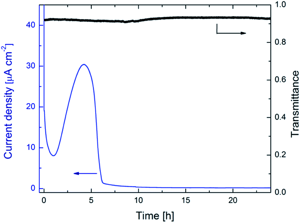 | ||
| Fig. 1 Evolution of current density (left-hand scale) and optical transmittance at a wavelength of 550 nm (right-hand scale) for a ∼300 nm-thick WO3 film immersed in LiClO4–PC and subjected to potentiostatic treatment at 6.0 V vs. Li/Li+. Arrows indicate applicable vertical scale. | ||
Materials analysis
For all ex situ measurements, the films were removed from the glove box, rinsed in 2-propanol and dried with nitrogen to eliminate electrolyte residues. Structural characterization of W oxide films was performed with X-ray diffraction (XRD) using a Siemens D5000 instrument working with Cu Kα radiation. Surface structures were investigated by scanning electron microscopy (SEM) employing a Zeiss 1550 FEG Gemini instrument with an acceleration voltage of 5 kV.X-ray photoemission spectroscopy (XPS) was conducted with a PHI Quantum 2000 Scanning ESCA Microprobe operating with monochromatic Al Kα1 radiation and having a beam diameter of 200 μm. Survey scans were taken for 0–1100 eV with pass energy of 117.4 eV and 1 eV resolution. High-resolution scans were obtained with pass energy of 23.50 eV and 0.025 eV resolution. Sample charging was avoided via a neutralizer filament. Adventitious carbon, with its 1 s peak at 248.8 eV, was used to calibrate spectra and correct for peak shifts due to charging. Elemental depth profiles during sputter etching were obtained with pass energy of 224.00 eV and 0.50 eV resolution.
Additional elemental depth profiles were obtained with time-of-flight elastic recoil detection analysis (ToF-ERDA), using 36 MeV 127I8+ primary ions, at the Tandem Accelerator Laboratory of Uppsala University. Technical details pertinent to the set-up are given in the literature.40 Time-of-flight/energy coincidence data were transformed to concentration profiles by use of the software CONTES.41 Elemental contents were also determined by Rutherford backscattering spectrometry (RBS) at the Uppsala Tandem Laboratory, using 2 MeV 4He ions backscattered at an angle of 170°. RBS spectra were fitted to a model for the film–substrate system via the SIMNRA program.42
Raman spectra were recorded with an inVia Reflex confocal Raman microscope (Renishaw, Gloucestershire, UK), using a 100× objective lens and 532 nm-wavelength laser and 2400 l mm−1 grating, in the wavenumber range of 100–2000 cm−1. Attenuated total reflectance Fourier transform infrared (ATR-FTIR) spectra were taken with a Bruker IFS 66v/S FTIR spectrometer equipped with a PIKE WeeMax III single reflection electro-ATR and a liquid-nitrogen-cooled HgCdTe detector. The spectroscopic measurements were performed in air with 4 cm−1 resolution.
Further details on thin-film preparation, experimental procedures and sample analysis can be found in earlier papers of ours.30,33,36
Results
Cyclic charge exchange and electrochromism
Fig. 2 presents our key electrochemical results and demonstrates that potentiostatic pretreatment of WO3 thin films gives a striking improvement of the cyclic charge exchange. Fig. 2a and a′ show cyclic voltammetry (CV) data for a potential window as wide as 1.5–4.0 V vs. Li/Li+ and at a sweep rate of 20 mV s−1 for, respectively, a film in as-deposited state and after potentiostatic pretreatment at 6.0 V vs. Li/Li+. Considering first the as-deposited film (Fig. 2a), it is apparent that rapid degradation occurs during 40 harsh CV cycles, which is consistent with earlier results.30,36 The potentiostatically pretreated film shows much better durability, and the CV data are almost cycle-independent (Fig. 2a′). The CV data are further analyzed in Fig. 2b and b′ which show data on inserted (Qinserted < 0) and extracted (Qextracted > 0) charge density as well as on charge imbalance δQ between successive insertion and extraction cycles, given by δQ = |Qinserted + Qextracted|. Initially, the as-deposited film has larger values of Qinserted and Qextracted than the potentiostatically pretreated one. However, the as-deposited film shows rapid declines in Qinserted and Qextracted upon CV cycling and the change is most pronounced around the 15th cycle (Fig. 2b). The potentiostatically pretreated film, on the other hand, displays much slower drops of Qinserted and Qextracted and the charge exchange (i.e., the average of Qinserted and Qextracted) becomes larger than for the as-deposited film after ∼15 CV cycles. Furthermore, there is no clear peak in δQ for the pretreated film (Fig. 2b′).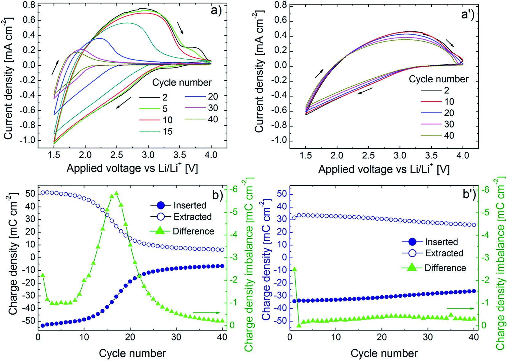 | ||
| Fig. 2 Electrochemical data for ∼300 nm-thick WO3 films immersed in LiClO4–PC. Panels (a) and (b) refer to as-deposited films and panels (a′) and (b′) to films that have been potentiostatically pretreated at 6.0 V vs. Li/Li+ for 24 h. Cyclic voltammograms in panels (a) and (a′) were recorded in LiClO4–PC after the indicated numbers of cycles at a sweep rate of 20 mV s−1; arrows indicate sweep direction. Inserted and extracted charge density, shown in panels (b) and (b′), were obtained from the data in panels (a) and (a′); panels (b) and (b′) also display difference in absolute value of charge density for successive charge insertions and extractions (individual data points are joined by straight lines for clarity). | ||
Electrochromism is intimately connected with charge insertion/extraction, and optical transmittance modulation mirrors charge exchange. Fig. 3a and a′ show mid-luminous transmittance for a WO3 film in as-deposited state and after potentiostatic pretreatment. The difference between the two sets of data is striking: the as-deposited film loses its transmittance modulation during the initial CV cycling in a fashion consistent with the earlier shown decline of charge exchange (Fig. 3a) whereas the potentiostatically pretreated film retains its electrochromism with only a minor deterioration of the optical modulation (Fig. 3a′). The effect of the potentiostatic pretreatment is manifested also in spectral optical data for the 400–780 nm wavelength range as seen in Fig. 3b and b′. Once again, it is evident that the electrochromism is rapidly lost upon CV cycling of the as-deposited film whereas the potentiostatically pretreated film has essentially cycling-independent optical performance. The optical properties of the as-deposited films agree fully with our earlier results.25,30–32,36
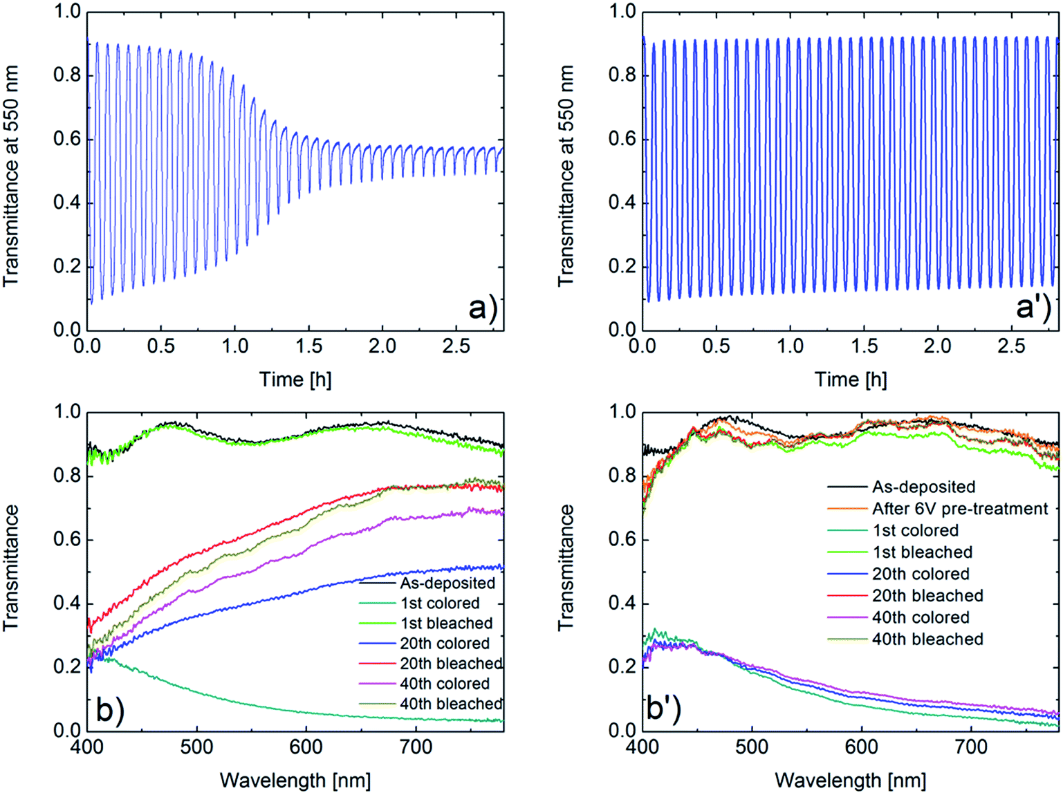 | ||
| Fig. 3 Optical data for ∼300 nm-thick WO3 films immersed in LiClO4–PC. Panels (a) and (b) refer to as-deposited films and panels (a′) and (b′) to films that have been potentiostatically pretreated in LiClO4–PC at 6.0 V vs. Li/Li+ for 24 h. Optical transmittance modulation at a wavelength of 550 nm is shown in panels (a) and (a′) and spectral optical transmittance after the stated number of ion insertion (coloring) and ion extraction (bleaching) cycles is shown in panels (b) and (b′); the optical data were taken in conjunction with the electrochemical measurements (some spectral data are partly overlapping). | ||
We also considered the role of potentiostatic pretreatment on the coloration efficiency (CE), which is a technically important property governing the efficiency of an electrochromic device and should be maximized for smart windows. The CE is given by ln(Tbleached/Tcolored)/ΔQ, where Tbleached and Tcolored are the transmittance of the film in its bleached and colored states, respectively, and ΔQ is the absolute value of Qinserted. As seen in Fig. S2,† the CE pertaining to a wavelength of 550 nm declines monotonically for the as-deposited film whereas it varies smoothly between 60 and 70 cm2 C−1 for the potentiostatically pretreated film and attains its largest values at the approach of 40 CV cycles.
Characterization of as-deposited and potentiostatically pretreated films
A wide range of characterization techniques was used in order to shed light on the crucial differences between as-deposited and potentiostatically pretreated samples. Structural characterization by XRD, reported in Fig. S3,† showed nothing but diffraction peaks due to the underlying ITO layer, implying that both types of WO3 films were amorphous. Morphological characterization was performed by SEM; Fig. S4† depicts micrographs of the surfaces of the two kinds of films and indicates that they are composed of aggregated ∼10 nm-size grains with interspersed cracks and crevices; no significant difference can be associated with the potentiostatic pretreatment. The images are consistent with those reported before for similarly prepared WO3 films.25XPS was used to determine elemental compositions for the films' surfaces, as well as depth profiles through the WO3 films down into the underlying ITO-coated glass substrate, in order to document differences between as-deposited and potentiostatically pretreated films. XPS survey scans are displayed in Fig. 4a and a′ for the surfaces of the two types of films and show features due to carbon, oxygen, tungsten and tin. Features due to indium on the surface were clearly seen only for the pretreated film. Corresponding atomic concentrations are reported in Table 1, which indicates that the WO3 film remains stoichiometric after the pretreatment. Moreover, it is found that the carbon concentration is decreased by about 20% as a result of the pretreatment and, interestingly, that the In concentration concurrently is more than doubled—from ∼0.3 to ∼0.7 at%—signaling that In diffusion through the WO3 film is promoted by the potentiostatic pretreatment.
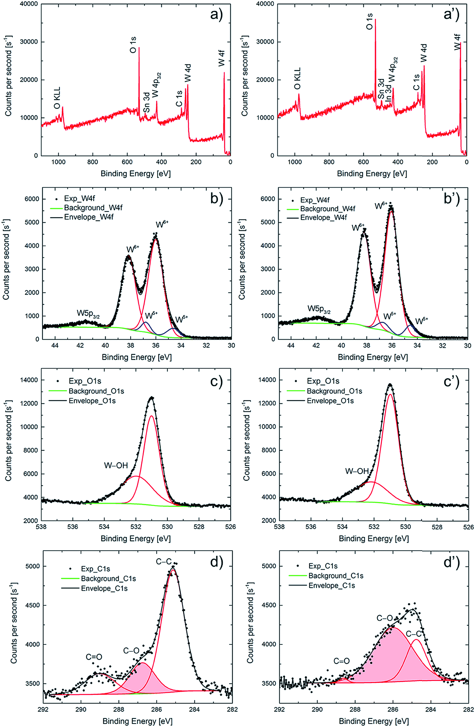 | ||
| Fig. 4 XPS count rate as a function of binding energy for ∼300 nm-thick WO3 films. Panels (a) and (a′) represent survey scans of a film in (a) as-deposited state and (a′) after potentiostatic pretreatment in LiClO4–PC at 6.0 V vs. Li/Li+ for 24 h. Panels (b) and (b′) are corresponding data specifically for the energy range pertaining to W 4f (and W 5p3/2 at ∼42 eV), panels (c) and (c′) refer to O 1s and panels (d) and (d′) refer to C 1s electrons. Electronic transitions are indicated in panels (a) and (a′), charge states are noted in panels (b) and (b′), and shaded bell-shaped areas in panels (d) and (d′) signify the stated chemical bonds. Dots represent measurements and curves are fittings, as described in the main text. Bottom curves in panels (b and b′), (c and c′) and (d and d′) mark backgrounds. | ||
| Atomic orbital | Binding energy (eV) | Atomic concentration (at%) | ||
|---|---|---|---|---|
| As-deposited | Potentiostatically pretreated | As-deposited | Potentiostatically pretreated | |
| C 1s | 284.8 | 284.8 | 29.6 | 23.2 |
| O 1s | 531.0 | 531.0 | 52.3 | 56.6 |
| W 4f | 17.1 | 18.5 | ||
| W5+ 4f5/2 | 36.8 | 36.7 | ||
| 4f7/2 | 34.6 | 34.5 | ||
| W6+ 4f5/2 | 38.2 | 38.1 | ||
| 4f7/2 | 36.1 | 36.0 | ||
| In 3d | 0.3 | 0.7 | ||
| In 3d3/2 | — | 452.5 | ||
| 3d5/2 | — | 445.2 | ||
| Sn 3d | 1.0 | 0.7 | ||
| Sn 3d3/2 | 494.0 | 494.4 | ||
| 3d5/2 | — | — | ||
High-resolution XPS spectra pertaining to spin–orbit split W 4f electrons are reported in Fig. 4b and b′. The binding energies of the W 4f5/2 and W 4f7/2 peak doublet are close to the values reported for WO3.43–45 Further quantification of the charge states of the tungsten atoms was accomplished by peak deconvolution (Fig. 4b and b′). Constraining the relative 4f5/2 and 4f7/2 peak areas to 3/4 and fitting the experimental data to Gaussian–Lorentzian peaks, the W5+/W6+ ratio was found to be 8% and 7% for as-deposited and potentiostatically pretreated films, respectively, showing that both films were predominantly comprised of stoichiometric WO3. The small feature at a binding energy of ∼42 eV is the 5p3/2 peak characteristic of WO3.44 The O 1s peak occurs at 531.0 eV (Fig. 4c and c′) as expected for WO3 and exhibits a small shoulder at 532.1 eV due to hydroxylation (W–OH).45
Importantly, it was possible to document a significant difference in the energy-resolved XPS spectra pertaining to C 1s electrons (Fig. 4d and d′) for as-deposited and potentiostatically pretreated films. There is general agreement in the literature on the assignment of the peaks in the C 1s region,46–48 and the C 1s spectra of both films could be deconvoluted into contributions from C![[double bond, length as m-dash]](https://www.rsc.org/images/entities/char_e001.gif) O at 288.7 eV, C–O at 286.0 eV and C–C at 284.8 eV. The C 1s signal from the as-deposited film is due mainly to adventitious aliphatic carbon contaminants with characteristic binding energy of 284.8 eV (used for internal energy calibration) due to C–C bonds (67% of the total integrated O 1s peak area). However, after the potentiostatic pretreatment, the relative magnitudes of the three bands were markedly different. Thus the C–O-derived peak at 286.0 eV became dominant (69% of the total integrated O 1s peak area) whereas the CO-derived peak at 288.7 eV shrank (peak area decreased from 15% to less than 3%). These results are consistent with the formation of a carbon-containing solid-electrolyte interfacial layer on the surface of the WO3 film comprising C–O species due to reactions with the electrolyte.
O at 288.7 eV, C–O at 286.0 eV and C–C at 284.8 eV. The C 1s signal from the as-deposited film is due mainly to adventitious aliphatic carbon contaminants with characteristic binding energy of 284.8 eV (used for internal energy calibration) due to C–C bonds (67% of the total integrated O 1s peak area). However, after the potentiostatic pretreatment, the relative magnitudes of the three bands were markedly different. Thus the C–O-derived peak at 286.0 eV became dominant (69% of the total integrated O 1s peak area) whereas the CO-derived peak at 288.7 eV shrank (peak area decreased from 15% to less than 3%). These results are consistent with the formation of a carbon-containing solid-electrolyte interfacial layer on the surface of the WO3 film comprising C–O species due to reactions with the electrolyte.
It should be noted that the carbonate-like layer existed only on the films' surfaces and XPS depth profile data, reported in the insets of Fig. 5, indicate that the C 1s atomic concentrations were low for as-deposited and potentiostatically pretreated WO3 films. The XPS data also showed clear signals due to W in WO3, In and Sn from ITO, Si from glass, and O from WO3, ITO and glass. Clear evidence for C was found only at sputter times less than 0.5 min and occurred along with increased O and decreased W signals. As shown in Fig. 5a, the WO3/ITO interface of the as-deposited film was quite distinct, and the signal due to W started to decrease at the same time as the In, Sn and O signals from ITO increased steeply after a sputter time of ∼73 min. The intensity due to In was very large and exhibited a maximum after ∼85 min, which was consistent with the location of the ITO/glass interface. Later, as the sputter-etch process continued, the signals from In and Sn decreased and the Si signal began to increase, as expected from ITO deposited onto glass. In contrast, after potentiostatic pretreatment (Fig. 5b), the intensities of the In and Sn signals were drastically reduced, indicating degradation of the ITO layer, and the WO3/ITO and ITO/glass interfaces became broadened. The In concentration profile shows that In penetrates into WO3 and also partly mixes with the glass along with W after pretreatment. The degradation of the ITO layer increases its resistance as clearly shown by electrochemical impedance spectroscopy (Fig. S5†). Specifically, the high-frequency resistance associated with ITO grows by almost a factor three after the pretreatment.
 | ||
| Fig. 5 XPS depth profiles for ∼300 nm-thick WO3 films, backed by ITO-coated glass, in (a) as-deposited state and (b) after potentiostatic pretreatment in LiClO4–PC at 6.0 V vs. Li/Li+ for 24 h. Insets show intensities due to the shown elements at the beginning of the sputter process. | ||
Complementary elemental depth profiling was carried out with ToF-ERDA and RBS, and Fig. S6† shows ERDA data for as-deposited and potentiostatically pretreated WO3 films. The atomic fractions for W and O are consistent with WO3 stoichiometry, the hydrogen content is ∼10 at% most likely emanating from OH− due to surface contamination, and there are trace amounts of nitrogen and carbon. A signal due to (In + Sn) was detected, although In and Sn could not be resolved individually; moreover the depth resolution of ERDA for these heavy subsurface species is poor. The composition profile of the WO3 layer for both samples is essentially depth-independent over the cross-sections as apparent from both ERDA data in Fig. S6† and the plateau exhibited by the signal due to W in the RBS spectra in Fig. 6. The latter figure shows experimental and simulated RBS data for as-deposited and potentiostatically pretreated WO3 films. The atomic masses of In and Sn are too close to allow separation of the signals from the individual elements. However, the data show clear evidence that the amount of (In + Sn) was reduced after potentiostatic pretreatment, which is consistent with the XPS depth profile data. Furthermore, the less deep minimum between the (In + Sn) and W areas, as well as the increased spread of the data points in the area associated with W, indicate that In atoms are able to penetrate into the WO3 layer during the pretreatment, as was also found from the XPS depth profile data.
 | ||
| Fig. 6 Experimental and simulated RBS spectra for a ∼300 nm-thick WO3 film in (a) as-deposited state and (b) after potentiostatic pretreatment in LiClO4–PC at 6.0 V vs. Li/Li+ for 24 h. Elemental compositions were determined by fitting experimental results (red dots) and simulated data (blue curves). | ||
SEM was used to acquire direct information on the films' cross-sections, and the data shown in Fig. 7 document structural modifications after the potentiostatic pretreatment. The as-deposited film exhibits two clearly visible layers: an upper porous film of WO3 with a thickness of ∼320 nm and a lower dense layer of ITO with a thickness of ∼50 nm. After the pretreatment, the WO3 layer became significantly thicker; the thickness was ∼380 nm, which may be due to a more porous structure developed during the In-intermixing process as well as to the carbonaceous interfacial layer formed on the surface of the WO3 film as indicated by the C 1s XPS spectra. Furthermore, the ITO layer became thinner and had a thickness of ∼37 nm.
 | ||
| Fig. 7 SEM cross-sectional images of a ∼300 nm-thick WO3 film, backed by ITO-coated glass, in (a) as-deposited state and (b) after potentiostatic pretreatment in LiClO4–PC at 6.0 V vs. Li/Li+ for 24 h. Scale bars are 100 nm. | ||
Vibrational spectroscopy was applied in order to further elucidate changes of the films during potentiostatic pretreatment and degradation, and complementary results were acquired for the ITO layer. Fig. 8a shows Raman spectra; the broad peak at a wavenumber of 770 cm−1 corresponds to symmetric and asymmetric ν(O–W–O) stretching modes, while the peak at 950 cm−1 can be assigned either to the ν(WO) stretching modes due to terminal oxygen atoms49–52 or to surface carbonates,53 or to combinations of these. After potentiostatic pretreatment of the uncycled film at 6.0 V vs. Li/Li+, the Raman spectrum was similar to the one for the as-deposited film. However, an up-shift and broadening of the band at 950 cm−1 indicate a higher carbonate content after pretreatment.53 Notably, the Raman spectrum of the pretreated film did not change significantly after 40 harsh CV cycles. Hence the data provide clear evidence that the O–W6+–O and W6+O bonds do not undergo significant alterations during the potentiostatic pretreatment and that deposited carboxylate/bicarbonate species are removed.
 | ||
| Fig. 8 (a) Raman and (b) ATR-FTIR spectra for ∼300 nm-thick WO3 films in the indicated states, for an ITO layer and for glass. CV denotes cyclic voltammetry, and diamonds in panel (a) refer to features due to ITO. Inset in panel (b) shows spectra confined to the 600–2000 cm−1 wavenumber range. The black line in (a) is drawn to show a small red-shift of the peak around 950 cm−1 after 6 V pretreatment. | ||
Analogous data taken by ATR-FTIR spectroscopy are reported in Fig. 8b with the aim to further establish carbonate formation at the electrolyte/film interface; it should be noted that ATR-FTIR spectroscopy is a more sensitive technique than Raman spectroscopy for these surface species. The as-deposited film showed a peak at ∼900 cm−1 corresponding to ν(WO) stretching vibrations and increased absorbance at wavenumbers below ∼800 cm−1 due to ν(O–W–O) vibrational modes.49,54 The ν(WO) peak became less distinct after electrochemical cycling. After the potentiostatic pretreatment, the absorbance of the film increased markedly and two peaks, associated with the glass substrate, emerged at 850 cm−1 and 750 cm−1. The appearance of these peaks may be attributed to a combination of decreased ITO thickness, deduced from SEM, and reduced extinction coefficient of the ITO layer due to lowered In concentration, as evidenced by In inter-diffusion into the WO3 film. The shoulder at ∼1050 cm−1 can be attributed to the TO phonon of the glass. Potentiostatic pretreatment at 6.0 V vs. Li/Li+ yields a peak at 1420 cm−1 which corresponds to C–O symmetric stretching vibrations of carbonates deposited on the WO3 surface.55 Water appears in the WO3 films as evidenced by the peaks at 1624 cm−1 due to δ(H–O–H) vibrations and the broad band between 3200 and 3500 cm−1 due to ν(O–H). Furthermore, after the pretreated film had undergone harsh electrochemical cycling it displayed almost the same ATR-FTIR spectrum as the one before the cycling thus indicating that there are no major changes of the film during the CV cycling after the pretreatment.
Discussion
This section attempts to consolidate our experimental results into a coherent picture describing the effects of the electrochemical pretreatment on the properties of the electrochromic films and especially on their durability. We first consider the influence of the pretreatment procedure. In preliminary measurements we applied high potentials, in an interval around 6.0 V vs. Li/Li+, to as-deposited WO3 films. The voltage window for achieving durability enhancement was found to be very narrow: 5.75 V vs. Li/Li+ was not sufficient whereas 6.25 V vs. Li/Li+ led to yellowish coloration of the electrolyte which indicated severe degradation. The origin of the current peak at ∼4.23 h in Fig. 1 is not entirely clear, although it is similar to a peak due to extraction of trapped Li ions during rejuvenation treatments, as mentioned above. Hence the peak seen in the present experiment is probably resulting from an ion-diffusion-related current, which could be due to In and Sn from the degradation of the ITO layer, as indicated in the XPS and RBS data. It is indeed known that ITO dissolves at high applied potentials in aqueous electrolytes,56 and a similar process is likely to occur in a LiClO4–PC electrolyte. In our case, however, the dissolution is partially hindered by the overlying WO3 layer so that inter-diffusion takes place among In, Sn and W species. Another contribution to the current observed during the potentiostatic pretreatment could ensue from side reactions in the electrolyte. It is known that the oxidation of propylene carbonate starts already at 4.5 V vs. Li/Li+ and is expected to be significant at 6.0 V vs. Li/Li+.57 Electrolyte degradation could also be the cause of the carbonaceous layer on the tungsten oxide, that was detected by XPS and ATR-FTIR. Such a layer would be kindred to solid-electrolyte interphases (SEIs) which are well-known in battery technology. The formation of organics-containing SEIs on battery cathodes at high potentials is firmly established experimentally but the details of their formation, and even their composition, are not well understood.58Several structural and compositional changes occur in the WO3 film during the potentiostatic pretreatment as evidenced by a number of characterization techniques. A decrease of the (In + Sn) content in the ITO layer after pretreatment was documented by both XPS and RBS. Evidently the ITO dissolves when subjected to potentials of the order of 6.0 V vs. Li/Li+,56 and (In + Sn) diffuses into the WO3 layer so that intermixing of the metallic constituents takes place. Concurrently there is a decrease of the ITO thickness, as evidenced by SEM, which leads to a higher resistance of the ITO layer as seen from impedance spectroscopy (Fig. S5†). In this context, we note recent work59 on the electrochemical properties of WO3 films backed by glass pre-coated with ITO as well as by indium–tungsten oxide (IWO) wherein it was reported that the maximum current density (oxidation peak) in the CV data shifted slightly towards higher potential upon extended cycling for samples containing IWO. This observation is consistent with our results in Fig. 2a′ and may lend some support to the inter-diffusion of W and In observed by XPS (Fig. 5). Another conspicuous structural change is related to carbonaceous surface layers, and electrochemical cycling of as-deposited WO3 films yielded carbonate deposits as indicated by C–O bonds observed by XPS and ATR-FTIR. The XPS depth profile (Fig. 5) showed that this surface layer is very thin; a rough estimate yields a thickness less than 5 nm (based on the sputter rate for the metal atoms, viz. ∼4 nm min−1).
It is not possible at this stage to formulate a detailed model on how the mentioned structural and compositional changes are related to the enhanced stability during electrochemical cycling. However, some remarks on possible contributing factors can be made. The mixing of In, and to a smaller extent Sn, into the WO3 layer might produce effects that are similar to those of Ti, which has a well-established ability to enhance the electrochemical stability of WO3 films17–22 presumably by stabilizing an amorphous structure. Evidence in favor of Sn addition to WO3 giving somewhat improved cycling durability can in fact be found in prior work on sol–gel-deposited films.60 Furthermore, the increased resistance of the ITO after pretreatment leads to a larger potential drop over the ITO film, thereby making the electrochemical cycling less harsh. A denser WO3 film is sometimes associated with higher electrochemical stability,27 but SEM showed a thickness increase after pretreatment which is sufficiently large that it is very unlikely to be due solely to the carbonaceous layer. Clearly, the protecting influence of the carbonaceous layer deserves attention in future studies.
To sum up, the increased electrochemical stability of WO3 films after pretreatment at high potential is likely due to a number of contributing effects: In (and Sn) intermixing in WO3, increased ITO resistance, and formation of a carbonaceous solid-electrolyte interface. The detailed characterization of as-deposited and potentiostatically pretreated films, presented in the present work, has narrowed down the range of possible causes for the electrochemical stability and has pointed out some directions for further studies.
Conclusions
The key result of the present work is that sputter deposited electrochromic tungsten oxide thin films are able to reach unprecedented electrochemical durability by potentiostatic pretreatment in LiClO4–PC at 6.0 V vs. Li/Li+ for several hours. These films maintain excellent optical modulation during repeated charge insertion/extraction, whereas as-deposited films of the same kind deteriorate rapidly under identical conditions. Our investigation provides new and significant information regarding physicochemical effects of potentiostatic pretreatment and demonstrates that pretreated WO3 films are not affected by Li+ ion accumulation during electrochemical cycling. Changes of the films were related to compositional differences at the WO3/ITO and ITO/glass interfaces with In inter-diffusion in the WO3 film, and to the formation of carbon-containing solid-electrolyte interfacial layers on top of the WO3. Our results may be crucial for evading ageing and degradation of WO3-based electrochromic devices and for the development of purposefully designed electrodes of relevance also for other ion-based devices.Conflicts of interest
There are no conflicts to declare.Acknowledgements
MAA thanks the Mexican Council for Science and Technology (CONACyT) for financial support to work at Uppsala University as a postdoctoral researcher. Complementary financing was received from the European Research Council under the European Community's Seventh Framework Program (FP7/2007–2013)/ERC Grant Agreement No. 267234 (GRINDOOR). HYQ is grateful for financial support from the China Scholarship Council Doctoral Joint-Training Program. Support by VR-RFI (contracts #821-2012-5144 & #2017-00646_9) and the Swedish Foundation for Strategic Research (SSF, contract RIF14-0053) supporting accelerator operation is gratefully acknowledged.References
- World Commission on Environment and Development, Our Common Future, Oxford University Press, London, UK, 1987 Search PubMed.
- N. Stern, The Economics of Climate Change: The Stern Review, Cambridge University Press, Cambridge, UK, 2007 Search PubMed.
- B. Obama, Science, 2017, 355, 126–129 CrossRef CAS PubMed.
- S. Pacala and R. Solocow, Science, 2004, 305, 968–972 CrossRef CAS PubMed.
- Buildings and Climate Change: Summary for Decision-Makers, United Nations Environmental Programme, Sustainable Buildings & Climate Initiative, Paris, France, 2009 Search PubMed.
- 2011 Buildings Energy Data Book, U.S. Department of Energy, Washington, DC, USA, 2012 Search PubMed.
- F. Favoino, M. Overend and Q. Jin, Appl. Energy, 2015, 156, 1–15 CrossRef.
- M. Pittaluga, in Eco-Efficient Materials for Mitigating Building Cooling Needs: Design, Properties and Applications, ed. F. Pacheco-Torgal, J. A. Labrincha, L. F. Cabeza and C. G. Granqvist, Woodhead, Cambridge, UK, 2015, pp. 473–497 Search PubMed.
- R. D. Clear, V. Inkarojrit and E. S. Lee, Energy Build., 2006, 38, 758–779 CrossRef.
- C. G. Granqvist, Handbook of Inorganic Electrochromic Materials, Elsevier, Amsterdam, The Netherlands, 1995 Search PubMed.
- G. B. Smith and C. G. Granqvist, Green Nanotechnology: Solutions for Sustainability and Energy in the Built Environment, CRC Press, Boca Raton, FL, USA, 2010 Search PubMed.
- Electrochromic Materials and Devices, ed. R. J. Mortimer, D. R. Rosseinsky and P. M. S. Monk, Wiley-VCH, Weinheim, Germany, 2015 Search PubMed.
- C. G. Granqvist, Thin Solid Films, 2014, 564, 1–38 CrossRef CAS.
- A. Llordes, E. L. Runnerstrom, S. D. Lounis and D. J. Milliron, in Electrochromic Materials and Devices, ed. R. J. Mortimer, D. R. Rosseinsly and P. M. S. Monk, Wiley-VCH, Weinheim, Germany, 2015, pp. 363–397 Search PubMed.
- C. G. Granqvist, M. A. Arvizu, İ. Bayrak Pehlivan, H.-Y. Qu, R.-T. Wen and G. A. Niklasson, Electrochim. Acta, 2018, 259, 1170–1182 CrossRef CAS.
- G. A. Niklasson and C. G. Granqvist, J. Mater. Chem., 2007, 17, 127–156 RSC.
- S. Hashimoto and H. Matsuoka, J. Electrochem. Soc., 1991, 138, 2403–2408 CrossRef CAS.
- S. Hashimoto and H. Matsuoka, Surf. Interface Anal., 1992, 19, 464–468 CrossRef CAS.
- J. Göttsche, A. Hinch and V. Wittwer, Sol. Energy Mater. Sol. Cells, 1993, 31, 415–428 CrossRef.
- F. S. Manciu, Y. Yun, W. G. Durrer, J. Howard, U. Schmidt and C. V. Ramana, J. Mater. Sci., 2012, 47, 6593–6600 CrossRef CAS.
- C. V. Ramana, G. Baghmar, E. J. Rubio and M. J. Hernandez, ACS Appl. Mater. Interfaces, 2013, 5, 4659–4666 CrossRef CAS PubMed.
- M. A. Arvizu, C. A. Triana, B. G. Stefanov, C. G. Granqvist and G. A. Niklasson, Sol. Energy Mater. Sol. Cells, 2014, 125, 184–189 CrossRef CAS.
- F. Lin, D. T. Gillaspie, A. C. Dillon, R. M. Richards and C. Engtrakul, Thin Solid Films, 2013, 527, 26–30 CrossRef CAS.
- J.-H. Zhang, G.-F. Cai, D. Zhou, H. Tang, X.-L. Wang, C.-D. Gu and J.-P. Tu, J. Mater. Chem. C, 2014, 2, 7013–7021 RSC.
- R.-T. Wen, G. A. Niklasson and C. G. Granqvist, ACS Appl. Mater. Interfaces, 2015, 7, 9319–9322 CrossRef CAS.
- Q. Liu, G. Dong, Q. Chen, J. Guo, Y. Xiao, M.-P. Delplancke-Ogletree, F. Reniers and X. Diao, Sol. Energy Mater. Sol. Cell., 2018, 174, 545–553 CrossRef CAS.
- S.-H. Lee, R. Deshpande, P. A. Parilla, K. M. Jones, B. To, A. H. Mahan and A. C. Dillon, Adv. Mater., 2006, 18, 763–766 CrossRef CAS.
- F. Lin, J. Cheng, C. Engtrakul, A. C. Dillon, D. Nordlund, R. G. Moore, T.-C. Weng, S. K. R. Williams and R. M. Richards, J. Mater. Chem., 2012, 22, 16817–16823 RSC.
- G. F. Cai, D. Zhou, Q. Q. Xiong, J. H. Zhang, X. L. Wang, C. D. Gu and J. P. Tu, Sol. Energy Mater. Sol. Cells, 2013, 117, 231–238 CrossRef CAS.
- R.-T. Wen, C. G. Granqvist and G. A. Niklasson, Nat. Mater., 2015, 14, 996–1001 CrossRef CAS PubMed.
- R.-T. Wen, C. G. Granqvist and G. A. Niklasson, ACS Appl. Mater. Interfaces, 2015, 7, 28100–28104 CrossRef CAS.
- R.-T. Wen, M. A. Arvizu, M. Morales-Luna, C. G. Granqvist and G. A. Niklasson, Chem. Mater., 2016, 28, 4670–4676 CrossRef CAS.
- R.-T. Wen, G. A. Niklasson and C. G. Granqvist, ACS Appl. Mater. Interfaces, 2016, 8, 5777–5782 CrossRef CAS PubMed.
- M. A. Arvizu, C. G. Granqvist and G. A. Niklasson, J. Phys.: Conf. Ser., 2016, 764, 12009 CrossRef.
- H.-Y. Qu, D. Primetzhofer, M. A. Arvizu, Z. Qiu, U. Cindemir, C. G. Granqvist and G. A. Niklasson, ACS Appl. Mater. Interfaces, 2017, 9, 42420–42424 CrossRef CAS PubMed.
- M. A. Arvizu, R.-T. Wen, D. Primetzhofer, J. E. Klemberg-Sapieha, L. Martinu, G. A. Niklasson and C. G. Granqvist, ACS Appl. Mater. Interfaces, 2015, 7, 26387–26390 CrossRef CAS PubMed.
- B. Baloukas, M. A. Arvizu, R.-T. Wen, G. A. Niklasson, C. G. Granqvist, R. Vernhes, J. E. Klemberg-Sapieha and L. Martinu, ACS Appl. Mater. Interfaces, 2017, 9, 16995–17001 CrossRef CAS PubMed.
- M. A. Arvizu, H.-Y. Qu, G. A. Niklasson and C. G. Granqvist, Thin Solid Films, 2018, 653, 1–3 CrossRef CAS.
- A. J. Bard and L. R. Faulkner, Electrochemical Methods: Fundamentals and Applications, Wiley, New York, USA, 1980, p. 143 Search PubMed.
- P. Ström, P. Petersson, M. Rubel and G. A. Possnert, Rev. Sci. Instrum., 2016, 87, 103303 CrossRef PubMed.
- K. S. Janson, CONTES: Conversion of Time–Energy Spectra: A Program for ERDA Data Analysis, Internal Report, Uppsala University, Sweden, 2004 Search PubMed.
- M. Mayer, AIP Conf. Proc., 1999, 471, 541–544 CrossRef.
- D. Gogova, K. Gesheva, A. Szekeres and M. Sendova-Vassileva, Phys. Status Solidi A, 1999, 176, 969–984 CrossRef CAS.
- A. V. Naumkin, A. Kraut-Vass, S. W. Gaarenstroom and C. J. Powell, NIST X-ray Photoelectron Spectroscopy Database 20, Version 4.1, National Institute of Standards and Technology, Gaithersburg, MD, USA, 2012, http://srdata.nist.gov/xps/ Search PubMed.
- M. Vasilopoulou, A. Soultati, D. G. Georgiadou, T. Stergiopoulos, L. C. Palilis, S. Kennou, N. A. Stathopoulos, D. Davazoglu and P. Argitis, J. Mater. Chem. A, 2014, 2, 1738–1749 RSC.
- M. T. Martínez, M. A. Callejas, A. M. Benito, M. Cochet, T. Seeger, A. Ansón, J. Schreiber, C. Gordon, C. Marhic, O. Chauvet, J. L. G. Fierro and W. K. Maser, Carbon, 2003, 41, 2247–2256 CrossRef.
- T. I. T. Okpalugo, P. Papakonstantinou, H. Murphy, J. McLaughlin and N. M. D. Brown, Carbon, 2005, 43, 153–161 CrossRef CAS.
- S. Kundu, Y. Wang, W. Xia and M. Muhler, J. Phys. Chem. C, 2008, 112, 16869–16878 CrossRef CAS.
- M. F. Daniel, B. Desbat, J. C. Lassegues, B. Gerand and M. Figlarz, J. Solid State Chem., 1987, 67, 235–247 CrossRef CAS.
- M. F. Daniel, B. Desbat, J. C. Lassegues and R. Gariem, J. Solid State Chem., 1988, 73, 127–139 CrossRef CAS.
- F. S. Manciu, J. L. Enriquez, W. G. Durrer, Y. Yun, C. V. Ramana and S. K. Gullapalli, J. Mater. Res., 2010, 25, 2401–2406 CrossRef CAS.
- D. Chatzikyriakou, N. Krins, B. Gilbert, P. Colson, J. Dewalque, J. Denayer, R. Cloots and C. Henrist, Electrochim. Acta, 2014, 137, 75–82 CrossRef CAS.
- K. Nakamoto, Infrared and Raman Spectra of Inorganic and Coordination Compounds, Part B, Wiley, Hoboken, NJ, USA, 6th edn, 2009 Search PubMed.
- S. Badilescu, P. V. Ashrit, F. E. Girouard and V.-V. Truong, J. Electrochem. Soc., 1989, 136, 3599–3602 CrossRef.
- A. Rodes, E. Pastor and T. Iwasita, J. Electroanal. Chem., 1994, 376, 109–118 CrossRef CAS.
- A. Kraft, H. Hennig, A. Herbst and K.-H. Heckner, J. Electroanal. Chem., 1994, 365, 191–196 CrossRef CAS.
- D. Pletcher, J. F. Rohan and A. G. Ritchie, Electrochim. Acta, 1994, 39, 1369–1375 CrossRef CAS.
- K. Xu, Chem. Rev., 2014, 114, 11503–11618 CrossRef CAS PubMed.
- A. Maho, S. Nicolay, L. Manceriu, G. Spronck, C. Henrist, R. Cloots, B. Vertruyen and P. Colson, J. Electrochem. Soc., 2017, 164, H25–H31 CrossRef CAS.
- H.-J. Ahn, H.-S. Shim, Y.-E. Sung, T.-Y. Seong and W. B. Kim, Electrochem. Solid-State Lett., 2007, 10, E27–E30 CrossRef CAS.
Footnotes |
| † Electronic supplementary information (ESI) available. See DOI: 10.1039/c8ta09621j |
| ‡ These authors contributed equally to the paper. |
| This journal is © The Royal Society of Chemistry 2019 |