
 Open Access Article
 This Open Access Article is licensed under a Creative Commons Attribution-Non Commercial 3.0 Unported Licence
Nickel-enhanced silver nanowire-based transparent heater with large size
Liwen Zhang†
,
Yanan Chen†,
Caiwei Xu,
Zhonggui Liu and
Yejun Qiu *
*
Shenzhen Engineering Lab of Flexible Transparent Conductive Films, Department of Materials Science and Engineering, Shenzhen Graduate School, Harbin Institute of Technology, Shenzhen, 518055, China. E-mail: yejunqiu@hit.edu.cn; qiuyejun2016@aliyun.com
First published on 18th April 2018
Abstract
An effective process for homogeneous electrodeposition of nickel was developed to improve the performance of silver nanowire-based transparent heaters (AgNW-THs). After electroplating Ni, the silver nanowires are uniformly coated by a layer Ni with 20–40 nm thickness, which has a small effect on the device transmittance, but significantly enhances its conductivity. Most excitingly, the nickel shell leads to a great increase of the temperature toleration of the AgNW-THs. A transparent tubular heater with large size of 3 cm in diameter and 20 cm in length is successfully fabricated, showing excellent heating properties in that the steady-state temperature can reach 284.3 °C and there is minimal variance in temperature after 10 heating cycles, and by using this tube, red Cu powder was oxidized into black CuO in a short time, which was visually observed. Additionally, two other shapes of transparent heaters with large size were constructed for dehydration of CuSO4·5H2O and burning of red phosphorus, respectively. This kind of transparent heater has wide applications requiring high transmittance, excellent temperature toleration and large size, especially for teaching experiment apparatus in a visual model.
Introduction
Transparent heaters (THs) are of great interest for their wide applications, such as window defrosters,1 outdoor panel displays, multimedia displays on windshields, military optics (such as shields, night vision devices, aircraft canopies and rifle scopes),2 etc. THs are a kind of device that can engender Joule heating due to the Joule effect when certain voltage is applied. So conductive materials are essential for the construction of THs. Currently, In–Sn oxide (ITO),3–5 as a typical transparent conductive material, has been widely used for vehicles, billboards, avionics and displays in the defrosting and demister applications.6,7 However, In is scarce and ITO-based devices are often expensive and can not match the requirement for flexibility in some cases, therefore an alternative is highly desired.Many researchers have proposed carbon nanotubes (CNTs), graphene, and Ag nanowires (AgNWs) as the most promising substitutes for ITO.8–14 However, for the CNTs, because of its larger contact resistance, the square resistance of the transparent conductive device is usually much greater than that of ITO,15 and the high resistance of CNT-based THs requires a higher input voltage, making this material not able to achieve a good tradeoff between conductivity and transparency and thus requiring a high bias to activate the device. As for graphene, some defects would cause some local hot spots, which lead to non-uniform heating of THs.16 What's more, in the process of synthesizing graphene, high temperature up to 1000 °C and high copper consumption lead to higher production cost.17,18
Comprehensively considering the requirement for low square resistance, high transmittance and excellent flexibility, the metal nanowire conductive network has been widely adopted to fabricate flexible THs.11,13,14,19–21 Among them, silver nanowires are most commonly used. For example, two THs based on AgNWs were fabricated by spin coating on glass and PEN substrates, respectively.21 At a voltage of 7 V, the devices could be heated to 55 °C.22 However, the size of the THs is very small. By using continuous roll-to-roll sputtering processes, two kinds of transparent heaters with polymer/metal/polymer (PMP) and polymer/metal/inorganic (PMI) structures on large-area PET substrates were constructed. PMP and PMI thin film THs exhibited excellent performance of reaching a temperature of about 100 °C in about 60 s and showing a uniform temperature distribution. These THs showed high potential in defrosting or temperature maintaining. Although certain progress has been achieved, the voltage required for heating to 180 °C is still too high when using AgNW-THs. More importantly, AgNWs would be destroyed when the heating temperature exceeds 180 °C.23 So the study of AgNW-THs bearing much higher heating temperature is of great significance.
It is difficult to fabricate heaters with different shapes, especially heaters with curved surface. Many methods were adopted to achieve this goal, for example electrohydrodynamic (EHD) jet printing,24 electrospinning combined with electroplating,25 and supersonic kinetic spraying technique.26 However, these methods require multiple steps, making the procedures more complicated and time-consuming. Moreover, due to the self-limitation of these methods, it is difficult to coat the dead corners of nanoheater to form an uniform distribution of temperature. Besides, the fabrication of large-size heaters is another difficult issue to be solved, which is mainly induced by inhomogeneity of conductive layer.
The main objective of this work is to fabricate novel AgNW-THs with extremely high temperature toleration and large size as well as relatively high transmittance being capable of visual teaching. So we adopted a simple method of dip-coating and modified electroplating to deposit a thin layer of Ni onto the AgNWs to form Ag@Ni core/shell structure to significantly improve the performance of AgNW-THs. A typical TH with 3 cm in diameter and 20 cm in length is successfully fabricated, showing bearing temperature of 284.3 °C. Finally three interesting examples were given, mainly aiming to visual teaching for chemical experiment.
Experimental
Chemicals and materials
AgNWs were purchased from Guangzhou Qian shun Industrial Material Co., Ltd, which were dispersed in ethyl alcohol with a concentration of 0.3 mg mL−1. Quartz substrate and ethanol were purchased from commercial suppliers. All chemicals were used without further purification. The solution for electroplating Ni was consisted of 1.33 M nickel sulfate, 0.35 M nickel chloride, and 0.1 M sodium citrate and the pH value was controlled at 4.Preparation of AgNW-based THs
Before electroplating Ni, the transparent substrate should be coated with a layer of AgNWs to gain certain conductivity, which is necessary for electroplating. The quartz substrate was cleaned in an ultrasonic ethanol bath for 30 min and dried in a vacuum oven. Thereafter, it was dip-coated with AgNWs and dried in the oven. And the AgNW-THs with the sheet resistance ranging from 20–100 Ω sq−1 were obtained.Electroplating Ni onto AgNW-based THs
During electroplating, the primary TH and foam nickel were used as the working electrode and counter electrode, respectively, and these two electrodes were connected with a DC power supply (MAISHENG, MS-605D) by commercial silver paste. The central axis of pristine AgNW-TH was perpendicular to the liquid surface of electrolyte and pulled back and forth with a speed of 0.4 cm s−1 along the axis during electroplating Ni. The electroplating was carried out at room temperature and the used parameters were different for the different substrates. In this paper, three substrates were adopted, including quartz tube with 3 cm in diameter and 20 cm in length, 50 mL three-necked flask and the quartz boat with 3 cm in width and 10 cm in length. Except of special statement, the electroplating voltage used for them was 1.5 V, 1.0 V and 1.3 V, respectively, and the electroplating time was 10 min, 3 min and 5 min, respectively. Here, in our work, a whole nickel film with less content of AgNWs can be formed under the condition of high electroplating voltage (1.5 V) and long deposition time (30 min), and was taken as pure nickel film.Device fabrication
To fabricate transparent heaters, copper foils were attached on two opposite edges of the Ni-enhanced AgNW-THs (Ni/AgNW-THs), and the silver paste was used to reinforce the mechanical and electrical connection between them. During tests, different voltages were supplied by a DC power supply. A thermal imager and a thermocouple were adopted to record the image of the temperature distribution and the change of temperature, respectively.Characterization
The samples were characterized by transmission electron microscopy (TEM/EDS, JEM 2010) and X-ray diffraction (XRD, Rigaku D/Max 2500/PC). The haze, transmittance and sheet resistance of the TCF samples were measured by a haze tester (SHANGHAI SHENGUANG INSTRUMENT, WGT-S), a UV-Vis spectrometer (SHIMADZU, UV-3600) ranging from 300–800 nm and a standard four point probe (KEITHLEY 6221/2182A). And the reported haze, transmittance and sheet resistance values were an average of the three measurements for haze, three measurements for transmittance at a wavelength of 550 nm and an average of six separated measurements for sheet resistance, respectively. And the temperature profiles on the surface of the nanoheaters were detected by a thermal imager (FLUKE, Ti45) and a thermometer (CENTER, 309).Results and discussion
In this work, a three-step procedure is adopted to fabricate the Ni-enhanced AgNW-based transparent heaters, as shown in Fig. 1. The first step is to obtain the AgNW-THs with good conductivity by dipping a substrate into a solution containing certain concentration of AgNWs. Generally speaking, the more the AgNWs deposit, the better the conductivity of the THs has, while the transmittance will decrease. Comprehensively considering the requirement in the conductivity, transmittance and large size of the final device, the concentration of AgNWs was well adjusted to obtain a suitable sheet resistance of 20–200 Ω sq−1. The second step is to further treat the AgNW-THs by electroplating Ni. The structure of the conductive Ni-coated AgNW layers can be well controlled through changing the electroplating parameters, mainly including the electroplating voltage and time. Interestingly, since the electrons firstly contact with Ni2+ through the interface between the substrate and liquid surface, the Ni is preferentially deposited at the upper position of the substrate. Because of the larger size, this phenomenon is even more obvious. Therefore, in order to obtain the uniform electrodeposition of Ni onto the whole substrate, the continuous movement of the substrate back and forth is designed, and after careful evaluation, the pulling speed is given at 0.4 cm s−1, as depicted in Fig. 1b. Pulling the cathode back and forth at a specific rate can not only increase the surface diffusion rate of the adsorbed nickel atoms but also accelerate the liquid phase mass transfer process and fully replenish the nickel ions in the cathode diffusion layer, thus resulting in high quality and large-size deposition of films.27,28 After electroplating Ni, the AgNWs are well protected by the coating and the AgNW-THs can possess low sheet resistance as well as high transmittance. In the last step, the heater devices were fabricated according to the procedures mentioned in the experimental section. At last, the properties of Ni/AgNWs-THs were investigated in detail.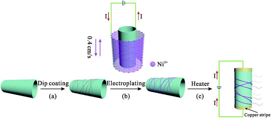 | ||
| Fig. 1 Schematic procedure for preparing THs: (a) deposition of AgNWs on transparent substrate by dip-coating; (b) electroplating Ni; (c) fabrication of TH device. | ||
Fig. 2 gives the TEM images, XRD patterns and EDS mapping of the AgNW before and after electroplating Ni. The initial diameter of the AgNWs is only about 40 nm (Fig. 2a), while the diameter after electroplating Ni increases to 60–100 nm (Fig. 2b), indicating the Ni shell layer with a thickness of 20–40 nm were encapsulated onto the AgNWs surface successfully. Excitingly, the deposited Ni leads to sharp decrease of the sheet resistance of the THs from 20–100 Ω sq−1 to 3–10 Ω sq−1. To further confirm the phase structure, Fig. 2c and d provide the XRD patterns of the two samples, and the diffraction peaks at 44°, 52° and 77° correspond to the crystal facets (111), (200) and (220) of face-centered cubic Ni, respectively. And the peak at 15–30° is caused by quartz glass substrate. Fig. 2e is the elemental maps, further testifying that the AgNWs are uniformly coated with Ni to form Ag@Ni core/shell structure, which is highly preferred for improving the temperature toleration.
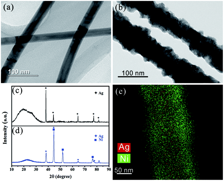 | ||
| Fig. 2 (a) Typical TEM image of AgNWs; (b) Typical TEM image of AgNWs after electroplating Ni; (c) XRD pattern of AgNW-THs; (d) XRD pattern of Ni/AgNW-THs; (e) elemental maps of Ni/AgNW sample. | ||
To deeply investigate the thermal property of the devices, three shapes of substrates with large size were selected, including quartz tube with 3 cm in diameter and 20 cm in length, 50 mL three-necked flask, and quartz boat with 3 cm in width and 10 cm in length. Fig. 3 presents their optical photos (Fig. 3a, c and e) and corresponding infrared thermal images (Fig. 3b, d and f). Clearly, all these TH devices exhibit high transmittance, and the inner situation of the substrate can be well observed, which is very important for visual teaching in chemical experiments. Moreover, from the infrared thermal images, it can be seen that the three THs can be heated to beyond 240 °C. Importantly, the temperature distribution on these substrates surface is very uniform, indicating the uniform electrodeposition of Ni onto the AgNWs.
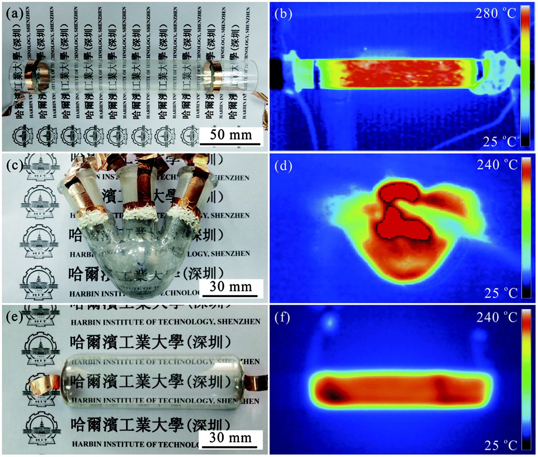 | ||
| Fig. 3 Optical photos (a, c, e) and corresponding infrared thermal images (b, d, f) of the Ni/AgNW-THs using different substrate: (a and b) quartz tube with 3 cm in diameter and 20 cm in length; (c and d) 50 mL three-necked flask; (e and f) quartz boat with 3 cm in width and 10 cm in length. | ||
Fig. 4a provides the transmittance spectra of different TH samples based on pure AgNWs, Ni-coated AgNWs, and Ni film. Clearly, after electroplating Ni on pure AgNW-TH with high sheet resistance, the transmittance of TH decreased from 90.6% to 81% and the sheet resistance decreased from 120 Ω sq−1 to 14 Ω sq−1. By modifying the electroplating process, these were improved to 82.8% and 13 Ω sq−1, respectively, which outperforms those of pure AgNW-TH with low sheet resistance (transmittance of about 79% and sheet resistance is about 15 Ω sq−1). To further evaluate the heating performance, the curves of the temperature evolution of the THs based on pure AgNWs, Ni-coated AgNWs, and Ni film are given in Fig. 4b–f. The temperature evolution of the pure AgNW-TH with low sheet resistance (haze is 4.2%) at applied voltages of 10–30 V shows a maximum temperature of about 169.9 °C (Fig. 4b), while the Ni film TH (sheet resistance is 4.9 Ω sq−1 and transmittance is 63%) shows a maximum temperature of about 472 °C after experiencing the same procedure (Fig. 4d), indicating the better temperature resistance. Fig. 4c gives the temperature evolution of the Ni/AgNW-TH prepared by normal electroplating (the sheet resistance is 14 Ω sq−1, the transmittance is 81%, and the haze is 10%) at voltages of 10–30 V, and this sample has a maximum temperature of about 213.2 °C, which is slightly higher than that of the pure AgNW-TH. To further improve the heating performance, the electroplating technique was modified into slowly pulling the substrate up and down at 0.4 cm s−1, and thus a TH with low sheet resistance of 13 Ω sq−1, transmittance of 82.8% and haze of 8% was achieved. When exerting the applied voltages from 10 V to 30 V, the heating temperature increases greatly and a steady-state temperature of 284.3 °C is obtained at 30 V (Fig. 4e), which increases about 115 °C in comparison to that of the pure AgNW-TH. A more detail comparison of THs in our work and other literatures is shown in Table 1, further demonstrating the high quality of THs obtained by this modified method. Moreover, the heating performance of this Ni/AgNW-TH can be well maintained even after 10 times heating–cooling cycles in the range of 50–220 °C at 25 V (Fig. 4f). To the best of our knowledge, this level is seldom reached in available literature.
 | ||
| Fig. 4 (a) Transmittance spectra of different THs: I–AgNW-TH with high sheet resistance; II-Ni/AgNW-TH fabricated by normal electroplating; III-Ni/AgNW-TH fabricated by slowly pulling substrates during electroplating; IV-AgNW-TH with low sheet resistance; V–Ni film fabricated by normal electroplating. (b) Temperature evolution of pure AgNW-TH as a function of applied voltages of 10–30 V; (c) temperature evolution of Ni/AgNW-TH fabricated by normal electroplating as a function of applied voltages of 10–30 V; (d) temperature evolution of Ni film fabricated by normal electroplating as a function of applied voltages of 10–30 V; (e) temperature evolution of Ni/AgNW-TH fabricated by slowly pulling substrates during electroplating as a function of applied voltages of 10–30 V (f) on/off response over 10 cycles of the Ni/AgNW-TH fabricated by slowly pulling the substrate under an applied voltage of 25 V. | ||
Noteworthy, the temperature evolution of AgNWs-based TH is uneven along with the increase of the voltage. To be specific, two temperature-rising sections can be observed at the voltage of 20 V, and the breaking point is around 120 °C (shown in side of Fig. 4b). The accelerating stage of heating up at this point indicates a great improvement of conductivity, which can be attributed to the thermal welding effect of AgNWs. However, the situation for nickel electroplated AgNWs is different. After electroplating, the welding effect of AgNWs would be diminished during the heat test due to the robust protection of Ni film, which can be confirmed by the smooth temperature-rising curve and uniform temperature increase (shown in Fig. 4c and e), indicating higher thermal stability of Ni/AgNW TH.
Finally, we provide three typical examples to testify the feasibility of the developed Ni/AgNW-THs. In this work, we chose large-size quartz tube (3 cm in diameter and 20 cm in length), three-necked flask (50 mL), and quartz boat (4 cm in width and 10 in length) as the substrates, respectively, due to their curved surface and common use in chemical lab. Fig. 5a shows the images of brownish 1 g red Cu powder before heating. When a DC input voltage of 30 V was supplied to the tubular Ni/AgNW-TH, the color of the powder changed gradually, and after heating for 300 s, the powder completely turned from red to black (Fig. 5b) according to the fact that red copper would be rapidly oxidized into black CuO at above 240 °C. Fig. 5c shows the photo of the blue CuSO4·5H2O before heating in a three-necked flask Ni/AgNW-THs. After heating at 30 V for 360 s, the 1.5 g CuSO4·5H2O turned into off-white anhydrous CuSO4 because of the dehydration of CuSO4·5H2O at about 260 °C (Fig. 5d). Furthermore, Fig. 5e exhibits the photo of red phosphorus powder before heating in a boat-shape THs. After heating at 30 V for 300 s, the 1.5 g red phosphorus burnt with white light and a lot of white smoke (Fig. 5f). These three application tests strongly indicate that the method developed here is suitable for the substrates with various shapes and the Ni-enhanced AgNW-THs have outstanding temperature toleration.
 | ||
| Fig. 5 Optical photos of different shape of Ni/AgNW-TH devices: Cu powder before (a) and after (b) heating at 30 V for 300 s in a tubular TH; CuSO4·5H2O before (c) and after (d) heating at 30 V for 300 s in a three-necked flask TH at 35 V for 360 s; red phosphorus powder before (e) and after (f) heating at 30 V for 300 s in the TH with a boat shape. | ||
Conclusions
In summary, we reported a simple but effective method to enhance the performance of AgNW-based THs by electroplating nickel. Especially, the substrates were slowly pulled back and forth, which would be preferred by uniform electrodeposition of Ni. And the Ni deposited onto the AgNW surface to form Ag@Ni nanowire structure, causing the contact resistance decreased greatly but negligible change in transmittance. Thanks to the excellent thermal resistance of Ni, some highly thermal stable Ni/AgNW-THs with large size were successfully fabricated. A tubular Ni/AgNW-TH can maintain the steady state temperature of 284.3 °C at 30 V, which is much higher than that (about 169.9 °C) of pure AgNW-TH. Moreover, the heating performance can be well maintained even after 10 times heating–cooling cycles in the range of 50–220 °C at 25 V. To the best of our knowledge, this level is seldom reached in the available literature. In addition, red Cu powder was oxidized into black CuO, blue CuSO4·5H2O was dehydrated into white CuSO4 and red phosphorus was burnt into P2O5, separately. These tests strongly indicated that the method developed here was suitable for the substrates with various shapes and the Ni-enhanced AgNW-THs had outstanding temperature toleration. This kind of transparent heater will possess wide applications in some areas requiring high transmittance, high heating temperature, curve shape, and large size, especially in visual teaching.Conflicts of interest
There are no conflicts to declare.Acknowledgements
The work was financially supported by Shenzhen Bureau of Science, Technology and Innovation Commission JCYJ20160525163956782 and JCYJ20170811154527927.Notes and references
- M. N. Gueye, A. Carella, R. Demadrille and J. P. Simonato, ACS Appl. Mater. Interfaces, 2017, 9, 27250–27256 CAS
.
- O. Ergun, S. Coskun, Y. Yusufoglu and H. E. Unalan, Nanotechnology, 2016, 27, 445708 CrossRef PubMed
- S.-M. Wie, C.-H. Hong, S. K. Oh, W.-S. Cheong, Y. J. Yoon and J. S. Kwak, Ceram. Int., 2014, 40, 11163–11169 CrossRef CAS
- P. D. Szkutnik, L. Rapenne, H. Roussel, C. Lachaud, V. Lahootun, F. Weiss and C. Jiménez, Surf. Coat. Technol., 2013, 230, 305–311 CrossRef CAS
- W. Ji, T. Wang, B. Zhu, H. Zhang, R. Wang, D. Zhang, L. Chen, Q. Yang and H. Zhang, J. Mater. Chem. C, 2017, 5, 4543–4548 RSC
- T. Sannicolo, M. Lagrange, A. Cabos, C. Celle, J. P. Simonato and D. Bellet, Small, 2016, 12, 6052–6075 CrossRef CAS PubMed
- R. Gupta, K. D. Rao, S. Kiruthika and G. U. Kulkarni, ACS Appl. Mater. Interfaces, 2016, 8, 12559–12575 CAS
- D. Kim, L. Zhu, D.-J. Jeong, K. Chun, Y.-Y. Bang, S.-R. Kim, J.-H. Kim and S.-K. Oh, Carbon, 2013, 63, 530–536 CrossRef CAS
- Z. Ding, Y. Zhu, C. Branford-White, K. Sun, S. Um-i-Zahra, J. Quan, H. Nie and L. Zhu, Mater. Lett., 2014, 128, 310–313 CrossRef CAS
- J. Kang, Y. Jang, Y. Kim, S. H. Cho, J. Suhr, B. H. Hong, J. B. Choi and D. Byun, Nanoscale, 2015, 7, 6567–6573 RSC
- S. Ji, W. He, K. Wang, Y. Ran and C. Ye, Small, 2014, 10, 4951–4960 CrossRef CAS PubMed
- D. Lordan, M. Burke, M. Manning, A. Martin, A. Amann, D. O'Connell, R. Murphy, C. Lyons and A. J. Quinn, ACS Appl. Mater. Interfaces, 2017, 9, 4932–4940 CAS
- H. Zhai, R. Wang, X. Wang, Y. Cheng, L. Shi and J. Sun, Nano Res., 2016, 9, 3924–3936 CrossRef CAS
- W. Lan, Y. Chen, Z. Yang, W. Han, J. Zhou, Y. Zhang, J. Wang, G. Tang, Y. Wei, W. Dou, Q. Su and E. Xie, ACS Appl. Mater. Interfaces, 2017, 9, 6644–6651 CAS
- J. Prasek, J. Drbohlavova, J. Chomoucka, J. Hubalek, O. Jasek, V. Adam and R. Kizek, J. Mater. Chem., 2011, 21, 15872 RSC
- D. Janas and K. K. Koziol, Nanoscale, 2014, 6, 3037–3045 RSC
- A. Reina, X. Jia, J. Ho, D. Nezich, H. Son, V. Bulovic, M. S. Dresselhaus and J. Kong, Nano Lett., 2009, 9, 30–35 CrossRef CAS PubMed
- C. Berger, Science, 2006, 312, 1191 CrossRef CAS PubMed
- T. Kim, Y. W. Kim, H. S. Lee, H. Kim, W. S. Yang and K. S. Suh, Adv. Funct. Mater., 2013, 23, 1250–1255 CrossRef CAS
- N. Kwon, K. Kim, J. Heo, I. Yi and I. Chung, Nanotechnology, 2014, 25, 265702 CrossRef PubMed
- J. Chen, Y. Li, W. Zhou, X. Feng, Q. Huang, J. G. Zheng, R. Liu, Y. Ma and W. Huang, Nanoscale, 2015, 7, 16874–16879 RSC
- C. Celle, C. Mayousse, E. Moreau, H. Basti, A. Carella and J.-P. Simonato, Nano Res., 2012, 5, 427–433 CrossRef CAS
- T. W. Kang, S. H. Kim, C. H. Kim, S. M. Lee, H. K. Kim, J. S. Park, J. H. Lee, Y. S. Yang and S. J. Lee, ACS Appl. Mater. Interfaces, 2017, 9, 33129–33136 CAS
- B. Seong, H. Yoo, V. D. Nguyen, Y. Jang, C. Ryu and D. Byun, J. Micromech. Microeng., 2014, 24, 097002 CrossRef
- H. S. Jo, S. An, J.-G. Lee, H. G. Park, S. S. Al-Deyab, A. L. Yarin and S. S. Yoon, NPG Asia Mater., 2017, 9, e347 CrossRef CAS
- J. G. Lee, J. H. Lee, S. An, D. Y. Kim, T. G. Kim, S. S. Al-Deyab, A. L. Yarin and S. S. Yoon, J. Mater. Chem. A, 2017, 5, 6677–6685 CAS
- R. P. Yang, X. Cai and Q. L. Chen, Surf. Coat. Technol., 2001, 141, 283–285 CrossRef CAS
- C. Wang, M. An, P. Yang and J. Zhang, Electrochem. Commun., 2012, 18, 104–107 CrossRef CAS
- R. Gupta, K. D. Rao, K. Srivastava, A. Kumar, S. Kiruthika and G. U. Kulkarni, ACS Appl. Mater. Interfaces, 2014, 6, 13688–13696 CAS
- J. Kang, H. Kim, K. S. Kim, S. K. Lee, S. Bae, J. H. Ahn, Y. J. Kim, J. B. Choi and B. H. Hong, Nano Lett., 2011, 11, 5154–5158 CrossRef CAS PubMed
- Q. Huang, W. Shen, X. Fang, G. Chen, J. Guo, W. Xu, R. Tan and W. Song, RSC Adv., 2015, 5, 45836–45842 RSC
Footnote |
| † These authors contributed equally. |
| This journal is © The Royal Society of Chemistry 2018 |