
 Open Access Article
 This Open Access Article is licensed under a
 Creative Commons Attribution 3.0 Unported Licence
Conductance in a bis-terpyridine based single molecular breadboard circuit†
Charu
Seth‡
a,
Veerabhadrarao
Kaliginedi‡
 *b,
Sankarrao
Suravarapu
b,
David
Reber
b,
Wenjing
Hong
c,
Thomas
Wandlowski
b,
Frédéric
Lafolet
d,
Peter
Broekmann
b,
Guy
Royal
*d and
Ravindra
Venkatramani
*a
*b,
Sankarrao
Suravarapu
b,
David
Reber
b,
Wenjing
Hong
c,
Thomas
Wandlowski
b,
Frédéric
Lafolet
d,
Peter
Broekmann
b,
Guy
Royal
*d and
Ravindra
Venkatramani
*a
aDepartment of Chemical Sciences, Tata Institute of Fundamental Research, Homi Bhabha Road, Colaba, Mumbai 400 005, India. E-mail: ravi.venkatramani@tifr.res.in
bDepartment of Chemistry and Biochemistry, University of Bern, Freiestrasse 3, CH-3012, Bern, Switzerland. E-mail: veera.kaliginedi@epfl.ch
cDepartment of Chemical and Biochemical Engineering, College of Chemistry and Chemical Engineering, Xiamen University, Xiamen 361005, China
dUniversité Grenoble Alpes, Département de Chimie Moléculaire, UMR CNRS-5250, Institut de Chimie Moléculaire de Grenoble, FR CNRS-2607, BP 53, 38041 Grenoble Cedex 9, France. E-mail: guy.royal@univ-grenoble-alpes.fr
First published on 3rd November 2016
Abstract
Controlling charge flow in single molecule circuits with multiple electrical contacts and conductance pathways is a much sought after goal in molecular electronics. In this joint experimental and theoretical study, we advance the possibility of creating single molecule breadboard circuits through an analysis of the conductance of a bis-terpyridine based molecule (TP1). The TP1 molecule can adopt multiple conformations through relative rotations of 7 aromatic rings and can attach to electrodes in 61 possible single and multi-terminal configurations through 6 pyridyl groups. Despite this complexity, we show that it is possible to extract well defined conductance features for the TP1 breadboard and assign them rigorously to the underlying constituent circuits. Mechanically controllable break-junction (MCBJ) experiments on the TP1 molecular breadboard show an unprecedented 4 conductance states spanning a range 10 −2G0 to 10 −7G0. Quantitative theoretical examination of the conductance of TP1 reveals that combinations of 5 types of single terminal 2–5 ring subcircuits are accessed as a function of electrode separation to produce the distinct conductance steps observed in the MCBJ experiments. We estimate the absolute conductance for each single terminal subcircuit and its percentage contribution to the 4 experimentally observed conductance states. We also provide a detailed analysis of the role of quantum interference and thermal fluctuations in modulating conductance within the subcircuits of the TP1 molecular breadboard. Finally, we discuss the possible development of molecular circuit theory and experimental advances necessary for mapping conductance through complex single molecular breadboard circuits in terms of their constituent subcircuits.
Introduction
The central goal in molecular electronics is to develop molecules as active electronic circuit elements.1,2 Towards this end, experimental techniques based on a Scanning Tunneling Microscope Break Junction (STM-BJ)3 or Mechanically Controllable Break Junction (MCBJ) have been developed to study molecular charge transport properties at a single molecule level.4–8 In STM-BJ/MCBJ, single molecules are contacted by two electrodes to form a metal–molecule–metal junction. Under the application of a bias voltage, the current flowing through the molecule, from one electrode to the other is sensitive to the molecular structure (length, conjugation pattern and conformation),9,10 the chemical nature of the linker which connects the molecule to the electrode,6,11–13 the relative position of linkers attached to the molecular core,14,15 the binding geometry of molecule between the electrodes,16–18 and the effect of external triggers on molecular structure and environment.2,6,19–22 Thus, these experimental techniques when combined with charge transport theory present a unique opportunity to create dynamic circuits with a library of molecules, which can act like wires,9,23–25 switches26,27 and diodes.21,28,29In conventional electrical and electronics engineering, solderless breadboard scaffolds are routinely used for quickly creating/testing a range of electrical circuits of varied complexity (Fig. 1A). Adapting the concept of breadboard on a molecular scale to prototype molecular circuits is an attractive idea. Aided by developments in synthetic methodologies, chemists are now able to synthesize large molecules incorporating different functional groups which in principle can form active or passive circuit elements. In order to develop the concept of a molecular breadboard circuit within a break junction framework, the choice of the chemical linker group is very important. The linker provides reliable attachment of molecules to the electrodes, determines the electronic coupling of the molecular core with the electrodes, and controls the range of relative orientations of the molecule with respect to the electrode. Experimentally, the conductance of organic molecules utilizing a number of anchoring groups have been compared including benzothiophene (–BT), pyridyl (–PY), amino (–NH2), thiol (–SH), isothiocyanide (–SCN), cyanide (–CN), nitro (–NO2), carboxylic acid (–COOH), dimethyl phosphine (–PMe2), methyl sulphide (–SMe), hydroxyl (–OH), and carbodithiolate based linkers.6,11–13,30 These studies have helped deconvolute the effect of the linkers from that of the molecular core on the single molecular junction conductance. Several experimental and theoretical attempts have been made to understand and/or predict the possible quantum interference patterns which govern the conductance properties of conductance pathways across the molecular core.14,31–37 These studies compared the relative conductance of molecules which differed in terms of either the chemical structure of the molecular core or the placement of anchoring groups within the molecule. In this context, the introduction of molecular breadboard circuits would be a significant advance, enabling the comparison of multiple conductance pathways within a single molecular scaffold. Indeed, steps have been taken towards realizing multiple circuits within a single molecular junction. Kiguchi and co-workers have recently demonstrated a conductance switch based on control of the molecule-electrode contacts within a quarterthiopene molecular junction with 4 thiophene anchoring groups.17 The authors captured 3 distinct conductance states and assigned it to bithiophene, trithiophene, and quarterthiophene circuits.17 Miguel and co-workers recently demonstrated 2 stable conductance pathways within a para-oligophenylene ethylene (p-OPE) molecular scaffold. By substituting the central benzene ring with sulfur and nitrogen heterocycles, the authors were able to demonstrate a new high conductance channel formed by the linking of the central pyrimidine ring to the electrodes.18 More recently, Kiguchi and co-workers have also shown the existence of 3 conductance states within a tripyridyl–triazine molecular junctions.38 In the studies above 17,18,38 single circuits were assigned to each conductance state observed in the experiments and upto 3 circuits across the molecular scaffold were proposed to be accessible by the experiments.
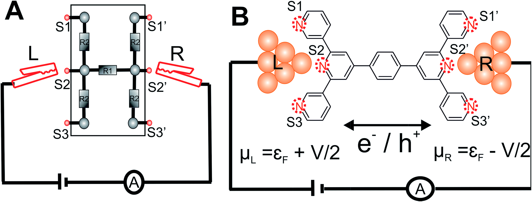 | ||
| Fig. 1 Enumeration of circuits within TP1 molecular breadboard: (A) schematic of a conventional electrical breadboard. For the breadboard depicted, multiple circuits of varying complexity can be created by throwing different permutations and combinations of the switches (S1-3, S1′-3′) (B) schematic of molecular breadboard junction formed for the TP1 molecule within a break-junction type setup. The TP1 molecular breadboard offers multiple circuits defined by the different contacts (S1-3, S1′-3′) made at nitrogen atoms by two electrodes. | ||
Here, we present the MCBJ implementation of a terpyridine based molecular breadboard (4′,4′′′′-(1,4-phenylene)bis(3,2′:6′,3′′-terpyridine), TP1), wherein multiple electrode anchoring pyridyl groups create 61 possible breadboard circuits within a single molecular scaffold (Fig. 1B). Further, each circuit has multiple thermally accessible conformations due to the molecular torsional flexibility. We experimentally capture 4 distinct conductance states for TP1 spanning 5 orders of conductance range as a function of electrode separation. A quantitative computational analysis of conductance and structures of over 1000 molecular circuits embedded within the TP1 breadboard reveals that the switching between different conductance states is controlled by accessing combinations of single and multi-terminal circuits within the breadboard. We find that the flexibility in molecular geometry imparted by the ring rotation degrees of freedom leads to less than one order of magnitude variation in the overall molecular conductance of TP1. Based on our analysis we are able to assign specific combinations of single terminal 2–5 ring circuits to each experimentally observed conductance state, estimate their percentage contribution to each state and extract their absolute conductance values. The role of quantum interference effects, thermal fluctuations, and possibility of formulating circuit rules for the TP1 breadboard are discussed.
Methods
Synthesis of TP1 and associated molecules
Details of the synthesis and characterization of all molecules examined in this manuscript are provided in Section S.1 of ESI.†Molecular junction conductance measurements
Single molecular conductance measurements were performed by employing home built mechanically controllable break junction set up. Further technical details of the MCBJ setup and data analysis procedures were reported in our previous publications.9,14,39 All the measurements were done in solution at room temperature. We provide more details in Section S.2 of the ESI.†Theory
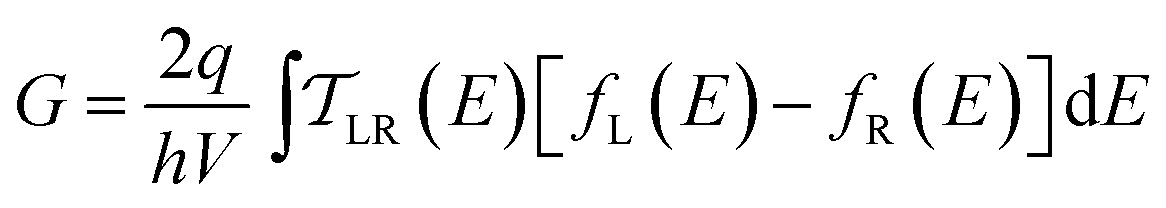
We use the framework of Non-Equilibrium Greens Functions (NEGF) to compute single molecule conductance of the TP1 molecule. The NEGF calculations are based on an INDO/s Hamiltonian and DFT optimized geometries of the molecule. This computational framework has been described in detail previously and shown to be effective in several previous studies of charge transport properties of small organic molecules.40–42 We outline the procedure for studying TP1 below. A more detailed description is provided in Sections S.3–S.5 of ESI.†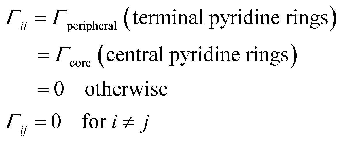 | (1) |
 | (2) |
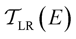 is computed from the INDO/S Hamiltonian as described previously and in Section S.5 of ESI.† The Fermi functions fL/R define the electron occupancy based on the chemical potentials μL/R (Fig. 1B) of left and right electrode:
 | (3) |
 | (4) |
| Contact configuration |
|
Examples |
|---|---|---|
| 1L–1R | (C16 × C15)/2 = 15 | 2-ring: L(S1′)–R(S2′) |
| 3-ring: L(S1)–R(S1′), L(S1)–R(S3) | ||
| 1L–2R or 2L–1R | C 2 3 × C14 = 12 (24 total) | 2-ring + 3-ring: L(S1, S2)–R(S3) |
| 2 × 2-ring: L(S1, S3)–R(S2) | ||
| 4-ring + 3-ring: L(S1, S3)–R(S2′) | ||
| 1L–3R or 3L–1R | C 1 3 × C33 = 3 (6 total) | 4-ring + 2 × 5-ring: L(S1)–R(S1′, S2′, S3′) |
| 3-ring + 4-ring + 5-ring: L(S1, S2, S3)–R(S2′) | ||
| 2L–2R | C 2 3 × C23 = 9 | 4 × 5-ring: L(S1, S3)–R(S1′, S3′) |
| 3-ring + 2 × 4-ring + 5-ring: L(S1, S2)–R(S1′, S2′) | ||
| 2L–3R or 3L–2R | C 2 3 × C33 = 3 (6 total) | 4 × 5-ring + 2 × 4-ring: L(S1, S3)–R(S1′, S2′, S3′) |
| 3-ring + 3 × 4-ring + 2 × 5-ring: L(S1, S2)–R(S1′, S2′, S3′) | ||
| 3L–3R | C 3 3 × C33 = 1 | 3-ring + 4-ring + 5-ring: L(S1, S2, S3)–R(S1′, S2′, S3′) |
The computational framework described here is not expected to reproduce absolute values of the experimental conductance due to the lack of knowledge of the exact form of the molecule-electrode coupling, uncertainty in the placement of the electrode Fermi level with respect to the molecular energy levels, and neglect of solvent in our models. However, as demonstrated previously, the framework can reliably reproduce relative trends in charge transport properties.40–42 Our calculations are thus expected to capture relative trends in the conductance of the circuits within the TPI molecular breadboard as a function of conformation and molecule-electrode contact configurations.
Our calculations neglect electronic correlations for metal electrodes which couple to the molecules. Such correlations can lead to interesting interference effects boosting or suppressing multi-terminal circuit currents relative to that obtained by a simple addition of currents from the constituent single terminal circuits.51,52 The neglect of correlated electron injection thus allows a simple decomposition of multi-terminal circuits into a superposition of single terminal circuits. Several considerations justify our choice of neglecting electron correlation between electrodes coupling to the TP1 molecule in the present study:
(1) Neither the gold coordination sphere around the nitrogen atoms of TP1 nor the shape of electrode tips interacting with the molecule is precisely known. Further, for the TP1 molecule the pyridine ring rotational degrees of freedom alter the relative positions of nitrogen atoms (see Fig. S5A†), such that even the closest nitrogen atoms located on adjacent pyridine rings (4–5 Å separation) may interact with distinct clusters of gold atoms.
(2) It is possible, of course, that nitrogen atoms on adjacent pyridine rings may share their gold coordination sphere for some TP1 geometries. However, in this case, the multi-terminal circuits are composed of asymmetric (in terms of number of aromatic rings) single terminal circuits with significantly different conductance values. For instance, in Fig. 1B the multi-terminal circuit L(S1, S2)–R(S1′, S2′) is composed of 3-ring (L(S2)–R(S2′)), 4-ring (L(S1)–R(S2′)/L(S2)–R(S1′)), and 5-ring (L(S1)–R(S1′)) circuits. Since such asymmetric circuits have very different conductance values (differing by 1–2 orders of magnitude; see Table 2 last row) any interference effects arising from correlated electronic injection at positions S1 and S2 would be negligible.
(3) Finally, for multi-terminal circuits with symmetric single terminal conductance pathways such as L(S1, S3)–R(S1′, S3′) or L(S1, S3)–R(S2), the relevant terminal nitrogen atoms (S1 and S3) are well separated (∼8 Å), and a model assuming independent electronic coupling at these positions is reasonable.
Results
Enumeration of the circuits in the TP1 molecular breadboard
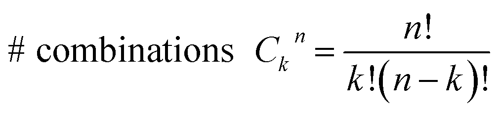
Consider a conventional macroscopic electrical breadboard circuit as shown in Fig. 1A, where different circuits can be created by contacting a pair of sockets (from S1, S2, S3, S1′, S2′, S3′) with two alligator clips. The number of possible 2 terminal circuits thus formed is C62 = 15 (where Ckn = n!/k!(n − k)! denotes the number of ways to pick k sockets from a set of n sockets). If we allow each of the two alligator clips to contact more than one socket, the breadboard can potentially offer up to 301 single and multi-terminal circuits (see Section S.4 in ESI† for detailed enumeration). Analogously, to enumerate circuits within the TP1 molecular breadboard (Fig. 1B), we consider the basic assumptions of two left (L) and right (R) contacting electrodes, circuits with symmetric transmission (IL→R(Vbias) = IR→L(Vbias)), and distinct sets of nitrogen atoms contacted by each electrode. Expressed in terms of the number of contacts (M, N) made by the two (L/R) electrodes, contact configurations (ML–NR, M, N = 1, 2, 3) can be symmetric (M = N) or asymmetric (M ≠ N). Here, we assume that a single electrode cannot contact pyridyl groups on both terpyridine arms of TP1 simultaneously. Further, in break junction experiments (e.g. MCBJ) the smallest electrode separation formed in a MCBJ experiment after breaking gold–gold contact (snap-back distance) is estimated to be ∼0.4–0.6 nm,9,11,12 which allows both symmetric and asymmetric circuits within each of the terpyridine arms of TP1. Under these constraints, 61 distinct circuits can be formed across the TP1 breadboard, which are enumerated in Table 1. We note that multi-terminal circuits can be decomposed into constituent single terminal circuits. For instance, the 1L–2R/2L–1R circuits can be decomposed (see Fig. 2) into two single terminal circuits which may be comprised of: (1) one 2-ring and one 3-ring circuit, (2) two 2-ring circuits, (3) one 4-ring and one 3-ring circuit, or (4) one 4-ring and one 5-ring circuit. These examples and other single and multi-terminal connections that are possible within a two electrode junction are summarized in Table 1 and Fig. 2. We will comment on the relationship between the currents from multi-terminal circuits and that from their single terminal constituent circuits in later subsections which discuss the conductance of the TP1 breadboard.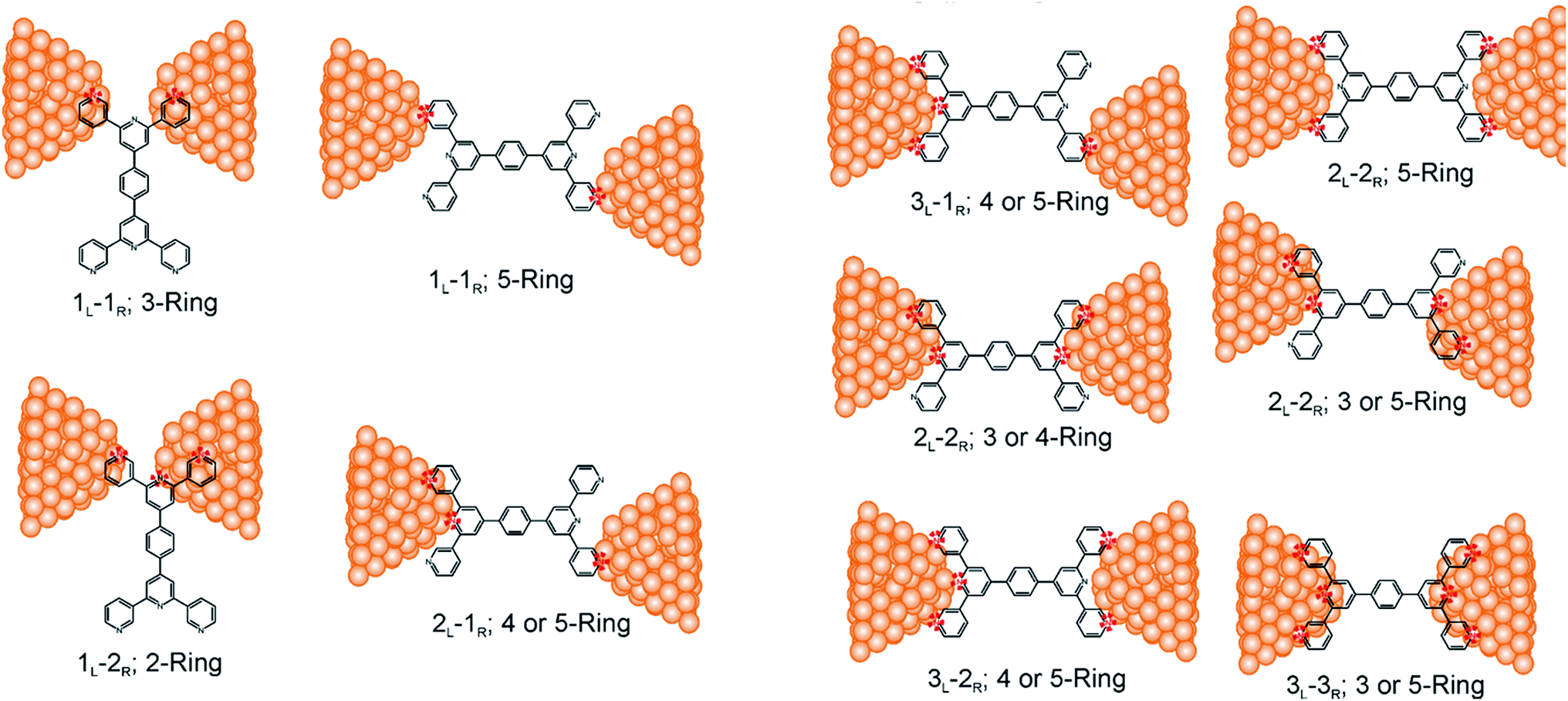 | ||
| Fig. 2 Examples of single and multi-terminal circuits for the TP1 that can potentially form in break junction experiments. Nitrogen atoms which are interacting with electrode are indicated in red color. | ||
A key feature of a molecular breadboard is that molecules can thermally populate multiple conformational states with distinct geometries and molecular conjugation, thereby dynamically creating new circuits with distinct conductance features. Thus, the molecular conformational space needs to be sampled for thermally accessible conformations. We therefore considered multiple optimized geometries of the TP1 molecule obtained from different starting conformations which differed in the relative orientations of the aromatic rings (see Methods and section). The 18 optimized TP1 geometries thus obtained were separated energetically by ∼3 kcal mol−1 (Fig. S5A in ESI†) and are accessible at room temperature. The optimized geometries of TP1 differ (Fig. S5A†) in the relative positions of nitrogen atoms in the two terpyridine subunits and the torsion angles between the pyridine rings and between the pyridine and benzene rings. The largest variation in nitrogen atom pair distances (∼2.5 Å) was seen for atoms located in different terpyridine units (inset of Fig. S5A†). Although we constructed the initial geometries of TP1 to have both, completely planar, and completely orthogonal orientations of adjacent terpyridine rings (see Methods and Section S.3 of ESI†), the optimized geometries showed a narrow range of torsion angles between adjacent pyridine rings of 25–30 degrees (Fig. S5B†) and pyridine benzene ring of 36–40 degrees (Fig. S5C†). Overall, all optimized structures exhibit similar π-conjugation with negligible differences in the HOMO–LUMO gap. To summarize, the energy landscape for the TP1 molecule shows multiple thermally accessible conformations which would contribute to the conductance in MCBJ experiments. However, preliminary evaluation of the electronic structure and geometric parameters suggests that the conformational heterogeneity would likely to have a modest effect on the molecular conductance of the TP1 molecular breadboard in break junction measurements.
Conductance measurements on the TP1 molecular breadboard
In order to measure conductance through all possible circuits of TP1 molecular breadboard, we employed a MCBJ set-up capable of operating in solution.9,11,39Fig. 3A shows typical conductance-distance traces obtained in the presence of TP1 as recorded in 1,3,5-trimethylbenzene (TMB)/tetrahydrofuran (THF) (4![[thin space (1/6-em)]](https://www.rsc.org/images/entities/char_2009.gif) :1, v/v). The breaking of atomic Au–Au contacts appears as plateaus observed in the conductance-distance traces in the range 1 ≤ G/G0 ≤ 10, where G0 = 2e2/h is the quantum of conductance. Additional plateaus appearing in the range 10−1G0 ≥ G/G0 ≥ 10−7.5G0. The noise limit of our MCBJ setup under the current experimental conditions is reached at 10−8G0. Fig. 3B displays the one-dimensional (1D) histogram on a logarithmic conductance scale as constructed from more than 1000 individual traces of TP1. The corresponding two-dimensional (2D) histogram of TP1 is shown in Fig. 3C. The individual conductance–distance traces were normalized to the common point Δz = 0 at G = 0.7 G0, which is characterized by a sharp drop in conductance immediately after breaking the last Au–Au monatomic contact upon pulling the leads apart. The quantitative analysis of the 1D and 2D histograms (Fig. 3B and C) reveals the existence of four well-defined conductance features for TP1 whereas no features were observed in experiments without TP1 molecules in solution (see Section S.2 in ESI†).
:1, v/v). The breaking of atomic Au–Au contacts appears as plateaus observed in the conductance-distance traces in the range 1 ≤ G/G0 ≤ 10, where G0 = 2e2/h is the quantum of conductance. Additional plateaus appearing in the range 10−1G0 ≥ G/G0 ≥ 10−7.5G0. The noise limit of our MCBJ setup under the current experimental conditions is reached at 10−8G0. Fig. 3B displays the one-dimensional (1D) histogram on a logarithmic conductance scale as constructed from more than 1000 individual traces of TP1. The corresponding two-dimensional (2D) histogram of TP1 is shown in Fig. 3C. The individual conductance–distance traces were normalized to the common point Δz = 0 at G = 0.7 G0, which is characterized by a sharp drop in conductance immediately after breaking the last Au–Au monatomic contact upon pulling the leads apart. The quantitative analysis of the 1D and 2D histograms (Fig. 3B and C) reveals the existence of four well-defined conductance features for TP1 whereas no features were observed in experiments without TP1 molecules in solution (see Section S.2 in ESI†).
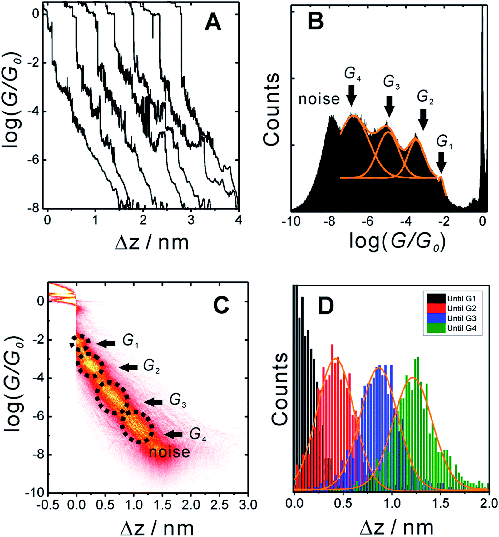 | ||
| Fig. 3 (A) Typical individual conductance versus relative displacement distance traces of TP1 recorded in MCBJ experiments in 1,3,5-trimethyl benzene (TMB)/tetrahydrofuran (THF) (4:1, v/v) containing 0.1 mM of the target molecules. (B) 1D logarithmic conductance histograms constructed from more than 1000 individual curves and recorded with a bias voltage of 0.10 V. (C) 2D conductance histogram. (D) Characteristic length 1D histograms analysed for G1, G2, G3 and G4. | ||
The presence of four distinct conductance features in the histograms of TP1 (G1, G2, G3 and G4 in Fig. 3) can be attributed to the sequential formation of different contact configurations between the molecule and the gold leads. Quantitative analysis of the 2D conductance (Fig. 3C) and characteristic length (Fig. 3D) histograms provided the following information: the high conductance state “G1” is observed as a conductance cloud in the range 10−3G0 ≤ G1/G0 ≤ 10−2G0 centered around the most probable value  at a relative lead displacement
  . Considering the snapback distance Δzcorr = (0.5 ± 0.1 nm) upon breaking of the monatomic Au–Au contact,9,11,53 we estimate an absolute most probable gap distance
  in the range of 0.45 nm to 0.65 nm. The second highest conductance state “G2” is observed in the range 10−4.5G0 ≤ G2/G0 ≤ 10−3G0 with the most probable value
 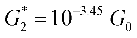 , and corresponding absolute gap distance
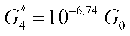
 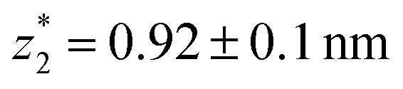 . Similarly, the next two conductance states G3 and G4 are seen in the range 10−6.5G0 ≤ G3/G0 ≤ 10−4.2G0 and 10−7.8G0 ≤ G4/G0 ≤ 10−6G0 and
 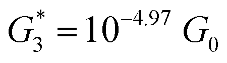 ,
,  respectively. The corresponding absolute most probable gaps for G2 and G3 conductance states are
  and
and  respectively. These data clearly demonstrate that the single molecular junction conductance of TP1 decreases in distinct steps upon pulling the gold leads apart and exhibits four conductance states.
Conductance calculations for the TP1 molecular breadboard
The origin of the conductance features produced in the experiments (Fig. 3) should be examined in the context of the 61 possible circuits enumerated for the TP1 molecular scaffold (vide supra) and their thermally accessible conformations. We thus carried out electronic structure calculations on the optimized TP1 geometries and Green's function based tunneling transport calculations (see Methods) for each single and multi-terminal molecular circuit enumerated in Table 1 within the 18 optimized geometries (1098 circuit calculations). In Fig. 4 we show the average conductance and associated standard deviations for each of the 61 circuits enumerated in Table 1 calculated across the 18 optimized TP1 geometries. The conductance of the single and multi-terminal circuits in the TP1 breadboard spans almost five orders of conductance values which matches the span of the experimental conductance range (10−2G0 to 10−7G0) in Fig. 3. | ||
| Fig. 4 Conductance features of the TP1 molecular breadboard circuits: average conductance (normalized with respect to the highest value) and variance over 18 optimized molecular conformations for the 61 circuits enumerated for TP1. The conductance data is coloured by the type of circuit as indicated and spread out across three bands. Fragments of TP1 whose circuits contribute to each band are shown in blue colour. Error bars where not visible are smaller than the symbols. | ||
Interestingly, the conductance values are distributed within 3 non-overlapping bands (gray color bands in Fig. 4), with the highest conductance band well separated from the remaining two. Each conductance band contains both single and multi-terminal circuits (colored by circuit type, ML–NR; M, N = 1, 2, 3) in Fig. 4. A striking feature of the conductance pattern in Fig. 4 is that the placement of circuits in each of the 3 conductance bands is independent of the number of contacts (single vs. multi-terminal) made by each electrode. In fact, multi-terminal circuit currents are only slightly higher (within a few fold) of corresponding single terminal currents within each conductance band. It can be shown (Section S.6 of ESI†) that for conditions (absence of correlated electronic injection, tunneling currents) assumed in this study, the currents from a multi-terminal circuit are simply a sum of single terminal currents. Thus, the three conductance bands in Fig. 4 can be primarily attributed to different single terminal circuits and their additive combinations (see Section S.6 of ESI†).
Each of the three conductance bands in Fig. 4 to correlate with the number of rings within contributing molecular circuits (see molecular fragments drawn in blue on the TP1 scaffold in Fig. 4 for each band). Circuits within the TP1 molecular breadboard can contain between 2–5 aromatic (purely pyridine, or a mix of pyridine and benzene) rings as shown in Table 1 and Fig. 2. The highest conductance band in Fig. 4 arises from contributions of 2-ring and 3-ring circuits within each terpyridine arm of TP1 (e.g. L(S1)–R(S2) and L(S1)–R(S3) from Fig. 1B). The second conductance band arises from primarily from 3-ring circuits comprising of the core pyridine-phenyl-pyridine branch (L(S2)–R(S2′) from Fig. 1B). The lowest conductance band arises from 4-ring circuits which comprise pyridine-pyridine-phenyl-pyridine branches (e.g. (L(S1)–R(S2′) from Fig. 1B) and from 5-ring circuits (e.g. (L(S1)–R(S1′) or (L(S1)–R(S3′) from Fig. 1B) which span both the terpyridine arms and include the central phenyl ring.
The variation in conductance values across the different geometries is modest, less than an order of magnitude. In our optimization protocol, we generated distinct geometries sampling the widest possible range of dihedral angles for TP1 (Section S.3 of ESI†). Nevertheless, the final optimized geometries showed a very narrow distribution of dihedral angles varying over a range of only ∼5 degrees (Fig. S5B and S5C†). Thus, this is the maximum variation in dihedral angles anticipated for thermally accessible TP1 conformations and leads to an overall variation in computed conductance of less than one order of magnitude (Fig. 4). In contrast, the experimental conductance distributions (Fig. 3) are much broader and cannot be explained in terms of variation in TP1 torsional flexibility alone. It is possible that the factors which are not included in our computational modeling, such as heterogeneity in the nitrogen–gold coordination geometries and the solvent effects may significantly contribute to broadening of the observed experimental conductance distribution.
Break junction experiments can access multiple circuits across a molecule with multiple electrode anchoring positions by changing the electrode separation.17,18,38 Experimental observables include conductance values and the most probable electrode separations at which they occur (Fig. 3C). Computationally we have access to the conductance of all 61 circuits (Fig. 4) of TP1 and their terminal nitrogen atom separations (Fig. S5A in ESI†). To convert the information in Fig. 4 and S5A† to a conductance vs. electrode separation plot, we propose a simple intuitive model: any circuit for which the terminal N–N atom separation (averaged over the 18 optimized conformations; see inset of Fig. S5A in ESI†) spans the electrode gap will contribute to the conductance of TP1 at that separation. For multi-terminal circuits the span of the shortest N–N separation distance is considered.
In Fig. 5 we plot the average conductance (calculated over 18 conformations) for all TP1 circuits (from the set of 61) which spans the junction gap as a function of electrode separation. Contributions from the specific single and multi-terminal circuits considered in Fig. 4 are separated out into different panels (the colors of symbols in each panel match those adopted in Fig. 4). The shaded region in each panel of Fig. 5 represents electrode separations (and corresponding conductance values) which are inaccessible to MCBJ experiments as they fall below the minimum estimated value of the electrode snapback distance (snap back distance ≈ 0.4–0.6 nm). Fig. 5 shows that all 61 circuits of TP1 are accessible to MCBJ experiments at short electrode separations (Δz < 0.4 nm). As the electrode separation increases from 0.4 nm to the full molecular length of 1.6 nm, the number of circuits contributing to the conductance of TP1 decreases as the terminal N–N atom separations for some circuits cannot span the junction gap. For instance, the highest conductance single terminal (1L–1R) circuit does not contribute to the TP1 conductance at electrode separations of 0.5 nm and beyond. Thus, as circuits drop out, the total conductance is expected to reduce in discrete steps as a function of electrode separation. The MCBJ experiment measures only the total conductance as a function of electrode separation (Fig. 3C) which can be obtained by summing up the conductance values from all circuits across the different panels in Fig. 5 at each electrode separation.
 | ||
| Fig. 5 Contribution of single and multi-terminal circuits to TP1 conductance as a function of electrode separation: in break junction experiments, different sets of circuits can be accessed by controlling the electrode separation. The different panels show average conductance (from 18 optimized geometries) contributions to the total conductance from different single and multi-terminal circuits (circuit notation and colours matching those in Fig. 4) whose terminal N–N distance (averaged over 18 optimized TP1 geometries) span the junction gap as a function of electrode separation (Δz). The shaded region indicates the conductance and electrode separations not accessible in MCBJ experiments as they lie below the estimated lower bound value of the snap-back distance (∼0.4 nm). | ||
Discussion
Our results demonstrate the potential of state-of-the-art break junction experiments in accessing multiple circuits within a single molecular scaffold. While the TP1 molecule contains a large number (61) of possible circuits, there are degeneracies in many conductance values (see Fig. 4) as well as the terminal distances (see inset of Fig. S5A in ESI†) for the circuits. Further, multiple circuits may contribute at a given electrode separation, reducing the number of distinct features captured in experimental conductance vs. electrode separation traces (4 peaks observed for TP1). In order to develop the concept of a molecular breadboard further, it is critical to map the experimental conductance features to the underlying contributing circuits. Note that a molecular breadboard is expected to have features distinct from a macroscopic electrical breadboard. First, molecules such as TP1 exhibit thermally driven conformational flexibility which can vary the conductance of individual circuits by an order of magnitude (Fig. 4) or more.10,54 Second, quantum interference effects can produce non-trivial additive effects of currents from multiple channels55,56 and make currents sensitive to the anchoring group positions on aromatic rings.14,31,57,58 In the following sections, we discuss circuit assignments for the experimentally observed conductance features and the effect of quantum interference and thermal fluctuations on the conductance of TP1. Finally, we also discuss the requirements for formulating circuit rules of molecular breadboard circuits. The analytical framework as well as key ideas developed here should be useful to interpret the data from experiments which examine multiple channels of charge flow within a single molecular scaffold.38Assignments of circuits to the experimentally observed conductance states
To derive the computed conductance vs. electrode separation plot shown in Fig. 5, we assumed a model wherein all circuits with terminal N–N distances equal to or larger than the junction gap contribute to the total TP1 conductance at that separation. Physically, since the molecule spans the gap, nitrogen atoms can coordinate with gold atoms located at the tip or further away from the gap (see Fig. 2 and S6A†). Using this model, Fig. 5 shows that for an electrode snap-back distance of Δzcorr = 0.4–0.6 nm (see Section S.2 in ESI† for an experimental determination),9,11,12 all 61 circuits contribute to the conductance and these circuit currents can be summed up to obtain the junction conductance at 0.4–0.6 nm electrode separation. As the electrode separation increases, circuits with terminal N–N distances shorter than the electrode separation drop out and the conductance is expected to reduce, thereby producing steps in conductance. For tunneling transmission, the relative contribution of various circuits are expected to be exponentially weighted by their terminal N–N distances. However, quantum interference and thermal fluctuations can significantly modulate the relative contributions of various circuits (vide infra). In Fig. 6 we plot the total junction conductance at each electrode separation (sum of conductance values from all contributing circuits across the 9 panels in Fig. 5) along with the experimental data (from Fig. 3C). Both computed and experimental data are normalized with respect to their corresponding highest conductance values in Fig. 6. The computed conductance is in excellent agreement with experimental data in terms of both, the overall range, and the drop of the conductance values with electrode separation validating our model. The computational model captures all four experimentally observed conductance states G1, G2, G3, and G4 and their correlation with electrode separation. The computational results suggest that there may be a fine structure to the G3 conductance profile near 1 nm which may not be resolved in the experiments. Further, the computational analysis indicates that the MCBJ experiments contact all 61 circuits and probe the full range of conductance values of the TP1 breadboard circuit within the experimentally accessible electrode separations (0.4–1.7 nm). In Fig. 6 we also show the dominant circuits contributing to each conductance state along with estimates of their percentage contribution. In the next paragraph, we further discuss how these circuits were assigned and their contributions estimated for each conductance state. | ||
| Fig. 6 Conductance map of TP1 molecular breadboard as function of electrode separation: comparison 2-D plots of computed total conductance from 61 circuits (red symbols) and master curve extracted from 2D-histogram of MCBJ measurements (black and white symbols). The 2D master curve was constructed by estimating the most probable conductance values from the Gaussian fits to cross sections of 2D histogram at different displacement positions Δz in Fig. 3c. The contributions of each of the 61 circuits to the computed total conductance were averaged over 18 optimized TP1 geometries. Since our computations only capture relative trends, both computed and experimental conductance values were normalized with respect to the conductance values at the smallest electrode separation (G1). Error bars for the computed conductance, where not visible, are smaller than the symbols. The dominant circuits (gold spheres indicate left/right electrode contacts) contributing to each conductance state are shown along with estimates of their percentage contribution to the total conductance at specific electrode separations where conductance steps occur. The shaded region indicates the conductance and electrode separations not accessible in MCBJ experiments as they lie below the estimated lower bound value of the snap-back distance (∼0.4 nm). | ||
From the data in Fig. 5 we find that a total of 61, 51, 49–53, and 5–9 single and multi-terminal circuits contribute to the computational G1, G2, G3, and G4 conductance states respectively. Note that we obtain a range of circuit combinations for the G3 and G4 conductance states as these states show a much stronger drop in conductance with electrode separation than the G1, and G2 conductance states (see also Fig. 6). Circuits can then be assigned to each conductance state based on the following two observations: (1) for the deep tunneling charge transport regime operational in TP1, the current from all multi-terminal circuit contributions can be decomposed into the sum of currents from all constituent single-terminal circuits, and (2) there are only 5 types of single terminal circuits (see Fig. 7A) present in TP1. These two conditions together imply that the total conductance of TP1 at each electrode separation can be expressed as a linear combination of currents (or conductance values) from the 5 single terminal circuits shown in Fig. 7A. In Fig. 7B, we show examples of the procedure to decompose two multi-terminal circuits with significant contributions to the total conductance of TP1 at an electrode separation of 0.4 nm into single terminal 2-ring and meta-3-ring circuits. We applied the decomposition procedure shown in Fig. 7B to express the current (conductance) from all contributing circuits in terms of the 5 types of single terminal circuits shown in Fig. 7A and estimated their relative contributions to the total conductance at each electrode separation. Further, the decomposition procedure also provides us with the total number of single terminal circuits contributing to a given conductance state. The circuits with the dominant contributions are shown in Fig. 6 and the detailed circuit assignments for the four conductance plateaus (G1, G2, G3, and G4) are presented in Table 2. Finally, coupling the information in Table 2 with the experimentally measured values for each conductance state and the percentage contribution to these states from the 2–5 ring circuits, absolute conductance values for each single terminal circuits assigned in Fig. 5 can be extracted. For instance, using the data in Table 2 and the measured G1 conductance, we can estimate the 2-ring circuit conductance to be: G(2-ring) = (0.81 × G1(experiment))/12. On the other hand the 3-ring circuit conductance can be estimated in two ways, (1) either using the experimental G1 value: (meta-3-ring) = (0.18 × G1(experiment))/6, or using the measured G2 conductance: G(meta-3-ring) = (0.90 × G2(experiment))/2. Estimates of absolute conductance values for all 5 single terminal circuits (2-ring, meta-3-ring, para-3-ring, 4-ring, and 5-ring) obtained by this procedure are listed in the last row of Table 2 along with the experimental conductance values from which they are drawn. Estimates for single terminal circuits calculated from multiple experimental conductance states were found to be consistent (differing by less than two fold in Table 2).
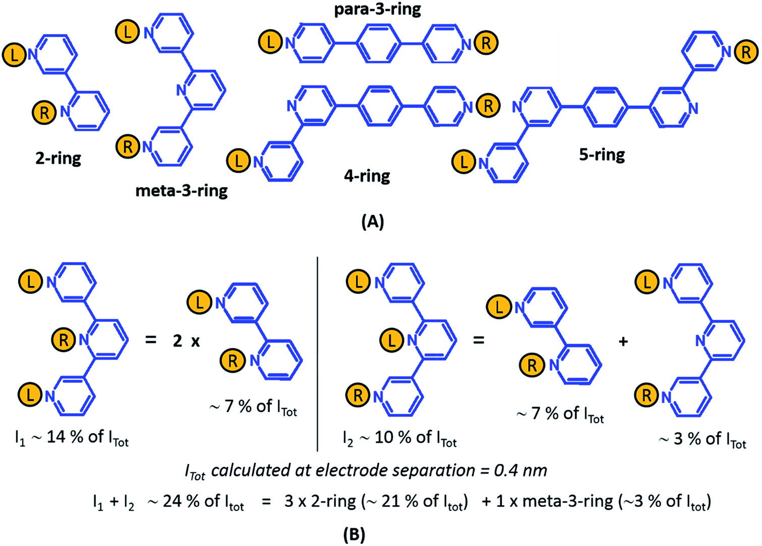 | ||
| Fig. 7 Decomposition of multi-terminal circuits into constituent single terminal circuits. (A) Five classes of single terminal circuits (gold spheres indicate left/right electrode contacts) present in the TP1 molecular breadboard. (B) Two of the highest contributing circuits (current I1 ∼ 14% and current I2 ∼ 10% contribution) to the total current Itot at electrode separation of 0.4 nm (Fig. 5 or 6) and their single circuit decomposition. I1 is a sum of currents from two 2-ring circuits. I2 is a sum of currents from one 2-ring circuit and one meta-3-ring circuit. Itot at electrode separation of 0.4 nm is obtained by summing up contributions from 61 such circuits (see Fig. 4B). In the example the current I1 + I2 amounting to 24% of Itot is a sum of currents from three 2-ring circuit (∼21% of Itot) and one meta-3-ring circuit (∼3% of Itot). | ||
| Conductance state | Contribution of single terminal (2–5 ring) circuits to each conductance state: number of circuits (percentage contribution to total conductance) | ||||
|---|---|---|---|---|---|
| 2-Ring | meta-3-Ring | para-3-Ring | 4-Ring | 5-Ring | |
| G 1 (0.4–0.5 nm) | 12 circuits (81%) | 6 circuits (18%) | 16 circuits (<1%) | 64 circuits (<1%) | 64 circuits (<1%) |
| G 2 (0.5–0.9 nm) | 0 | 2 circuits (90%) | 16 circuits (6%) | 64 circuits (3%) | 64 circuits (<1%) |
| G 3 (1.0–1.1 nm) | 0 | 0 | 16 circuits (62%) | 64 circuits (32%) | 64 circuits (6%) |
| G 3 (1.2–1.4 nm) | 0 | 0 | 0 | 32 circuits (79%) | 48 circuits (21%) |
| G 4 (1.6 nm) | 0 | 0 | 0 | 0 | 7 circuits (100%) |
| G (single-terminal) estimates | (G1) 4.25 × 10⁻⁴G0 | (G1) 1.89 × 10⁻⁴G0 | (G2) 1.35 × 10⁻⁶G0 | (G2) 2.16 × 10⁻⁷G0 | (G3 – 1.2 nm) 4.81 × 10⁻⁸G0 |
| (G2) 1.62 × 10⁻⁴G0 | (G3 – 1.2 nm) 2.72 × 10⁻⁷G0 | (G4) 2.57 × 10⁻⁸G0 | |||
The conductance plateaus in Fig. 3 and 6 drop exponentially with distance. By plotting the most probable conductance values extracted from the 1D conductance histogram (Fig. 3B) as a function of electrode separations extracted from characteristic length histogram (Fig. 3D), we estimated an experimental tunneling decay constant as βExperiment = 3.4 nm−1 (Section S.9 of ESI†). Since the theoretical analysis in this section assigns specific dominant 2–5 ring single terminal circuits to each conductance plateau in Fig. 6, we also plotted the theoretically calculated conductance of the dominant circuits as a function of electrode separation (Fig. S11B†). The conductance from dominant circuits drops exponentially with increase in the number of rings of the circuits with a decay constant of βTheory = 3.8 nm−1 (Section S.9 of ESI†). The decay constant values extracted from both the experiment and theory are in similar range with the decay constant values reported previously for oligophenyls (OP: 3.5–5 nm−1), OPE (2.0–3.4 nm−1), and oligophenyleimine (OPI: 3 nm−1).6 However, we stress that the interpretations of tunneling decay constants for circuits embedded within a molecular scaffold is different and more complex than that for isolated circuits. For instance, the drop in TP1 junction conductance occurs not only due to a change in the dominant circuit (increasing number of rings) with electrode separation, but also due to a drop in the number of contributing circuits (see Fig. 5). Further, the dominant circuits within TP1: (1) are composed of mixture of pyridine and phenyl rings, (2) do not have linear ring connectivity, and (3) differ in their ring connectivity positions (ortho/meta/para) to the electrodes. The next section sheds further light on the relative conductance values of the dominant circuits assigned in Fig. 6 and how they shape the observed conductance features of TP1.
Quantum interference effects and their manifestations in the conductance features of TP1
Several studies have reported quantum interference effects in molecular junctions.14,31,41,57,58 Xing et al. found that phase cancellation of currents through molecular orbitals of opposite symmetry diminished the contribution of frontier orbitals to both electron and hole transport in OPE molecules.41 Arroyo et al. found interference effects between charge transport pathways through HOMO and LUMO of a benzene ring coupled to thienyl anchoring units through ethynyl spacers.57 Further, anchoring group placement at ortho-, meta-, or para-positions of six membered rings have been shown to significantly modulate the conductance of conjugated systems.14,58The dominant 2–5 ring circuits assigned to the TP1 junction conductance at different electrode separations show diverse terminal nitrogen placements, and in this section we examine interference effects in these circuits. For each 2–5 ring embedded fragment of TP1, we computed conductance for electrode electronic couplings with atoms at para-, meta-, and ortho-positions of the pyridine rings of the molecule (see markings for each circuit in Fig. 8). Note that all 2–5 circuit conductance computations (Methods) use the full TP1 Hamiltonian (i.e. calculations are on embedded circuits). In order to cover the three para-, meta-, and ortho-connectivities for each 2–5 ring fragment, we considered carbon atom terminated circuits in addition to the dominant circuits assigned in the last section. While, previous studies have suggested that the electrode can couple to the carbon backbone through the π orbitals.6,8,14,59–61 It is not our intent to explore the through space coupling effect here. Rather, the carbon terminated circuits serve as surrogates of nitrogen terminated circuits to assess the effect of ring-electrode connectivity on the conductance of each 2–5 ring embedded fragment of TP1. In Fig. 8 we plot average values and standard deviation for single terminal circuit conductance values sampled across the 18 different optimized geometries of TP1.
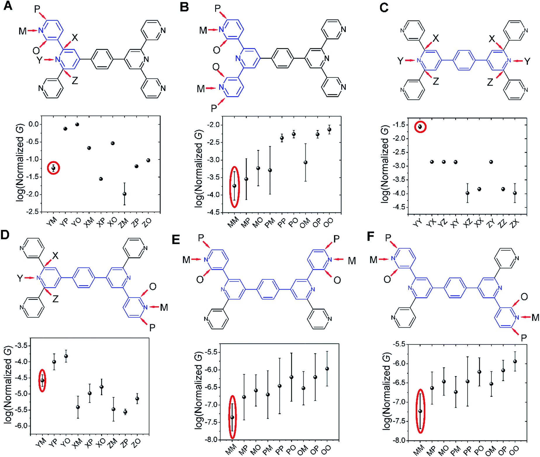 | ||
| Fig. 8 Quantum interference effects in TP1 molecular breadboard: the six panels (A–F) show single terminal conductance values (average and standard deviation from 18 different optimized geometries for each circuit) for 2–5 ring embedded fragments within TP1. All conductance values were normalized with respect to the highest conductance for the 2-ring circuit in panel (A). The 2–5 ring circuits corresponding to each panel are highlighted in blue over the TP1 scaffold. The positions of atoms electronically coupled to the left and right electrodes are labelled as para (P), meta (M), and ortho (O) with respect to the connectivity to the adjacent ring. Since the central ring of each terpyridine arm is connected to two terminal pyridine rings and also to the central benzene ring, the electrode contacts for the central pyridine ring of each terpyridine unit are labelled as X, Y and Z. For a 2-ring circuit (panel A) Y = ortho, Z = meta and for 3-ring/4-ring circuits X = Z = meta and Y = para. In our calculations all molecule-electrode electronic couplings have the same value (Γ = 0.1 eV). The data circled in red are from dominant 2–5 circuits assigned for the TP1 conductance states (Fig. 6). Note that the normalization for all panels is with respect to the highest conductance values in panel (A), which are for carbon terminated circuits which are not considered in the calculations in Fig. 4–6. Further, the electrode accessibility of all nitrogen atoms is not the same for TP1 (see eqn (1) in Methods). Thus the range of conductance values is larger than that for the data in Fig. 4–6. | ||
Following only the conductance values of the dominant 2–5 ring systems (red circles) across the panels, we find Gavg(2-ring) ∼ Gavg(para-3-ring) ≫ Gavg(meta-3-ring) > Gavg(4-ring) ≫ Gavg(5-ring). Clearly, the conductance drop with electrode separation does not correlate with the increase in the tunneling length (number of aromatic rings) of the dominant circuits contributing to the conductance at increasing electrode separations. The data in Fig. 8A and C show that quantum interference effects can lead to significant overlaps in the conductance ranges for molecular circuits of different length: the optimally placed para anchors produce the highest possible para-3-ring conductance (Fig. 8C), while the sub-optimally placed meta and ortho anchors produce a weak 2-ring conductance (Fig. 8A). Thus, if all nitrogen atoms had the same accessibility to the electrodes, the TP1 breadboard would produce nearly degenerate G1 and G2 conductance values at the first two electrode separations (see for example Fig. S9†). Thus, quantum interference can produce tunneling length independent conductance features in the TP1 breadboard. However, these signatures of quantum interference do not manifest in the experimental conductance vs. distance plots (Fig. 3C or 6). The nitrogen atoms of the central pyridine ring of the terpyridine units (core nitrogen atoms) are not as accessible to the electrode as nitrogen atoms of the peripheral pyridine rings. Based on a structural analysis on the optimized geometries of TP1, we estimate (see Discussion following eqn (1) in Methods) an effective ∼100 fold reduction in the electronic coupling for the core nitrogen atom relative to the peripheral nitrogen atoms of each terpyridine ring. In this case, the G2 conductance primarily arising from the 3-ring circuit (core nitrogen atoms at both terminals) in Fig. 7C is lowered relative to the G1 conductance primarily arising from the 2-ring circuit (only one terminal core nitrogen) as observed in the experiments (Fig. 3C). We present plots of the transmission for the dominant 2–5 ring circuits in Fig. S12 of ESI.† The plots reveal weak interference features due to the effect of conformational fluctuations for meta-3-ring circuits. Other circuits also show weak interference features as they are do not have meta terminated contacts at both ends.
In Fig. 8, we find that the lowest currents generally come from circuits which involve at least one meta-anchoring group position and the highest currents involve an ortho-/para-anchor. For instance, in 2-ring circuits (Fig. 8A), the average conductance: Gavg(YP/YO) ≫ Gavg(ZM). In the 3-ring circuits of Fig. 8B and C, we find Gavg(PP) ≫ Gavg(MM) and Gavg(YY) ≫ Gavg(XX/ZZ/XZ) respectively. We find that the effect of the anchoring group ring position on circuit conductance is preserved even when the terminal electrode contacting pyridine rings are separated by intervening aromatic rings. For instance, in 4-ring circuits (Fig. 8D), we find Gavg(YP) ≫ Gavg(XM/ZM) and in 5-ring circuits (Fig. 8E and F) we find Gavg(PP) ≫ Gavg(MM). In accordance with previous reports,14 we find higher currents for para-3-ring circuits relative to that for meta-3-ring systems (Gavg(PP) in Fig. 8B ≪ Gavg(YY) in Fig. 8C). Other trends get washed out due to variations in conductance which arise from the torsional flexibility of TP1. The largest variations in conductance are seen for 5-ring circuits (Fig. 8E and F) which wash out the conductance differences for para-, meta-, and ortho-terminated circuits. In contrast, conductance data for the 2- and para-3-ring circuits in Fig. 8A and C show much smaller fluctuations with well resolved conductance features. While 4-ring circuits (Fig. 8D) also show significant conductance fluctuations, two classes of conductance values are resolved; the YP (para–para) and YO (para–ortho) circuits show higher conductance values relative to the other circuits. The meta-3-ring terpyridine circuit in Fig. 8B also exhibits two cleanly resolved classes of circuits with low conductance and large fluctuations for at least one meta-anchor (MM, MP, MO, PM, and OM) and high conductance with low fluctuations for ortho-/para-anchors (PP, PO, OP, and OO). To summarize, we find that after including the effects of conformational heterogeneity, the modulation of conductance due to quantum interference is cleanly resolved for 2-ring and para-3-ring circuits (Fig. 8A and C), partially resolved for the meta-3-ring and 4-ring circuits (Fig. 8B and D), and washed out for the 5-ring circuits (Fig. 8E and F).
The results in this section show that the TP1 molecular breadboard offers several circuits with coherent quantum conductance features. However, physical considerations such as the variable accessibility of the anchoring groups to the electrode and conductance fluctuations from the torsional flexibility of the molecule mask the signatures of quantum interference leading to the observed conductance features in Fig. 6. We also note that other factors not explored here, such as through space electronic coupling of electrode to the carbon backbone through the π orbitals,6,8,14,59–61 could also limit the modulation of observed conductance through quantum interference effects.
Towards formulation of circuit rules for molecular breadboard circuits
Predicting the conductance through a molecular circuit in terms of transport properties of individual molecular components is an unsolved fundamental challenge in field of molecular electronics. From elastic scattering theory, transport through a molecular super circuit formed by binding two oligomers with transparencies T1 and T2 in series is proportional to T1 × T2.55,62,63 In accordance with this rule, several molecular wires show additive decay constants with increase in molecular length.9,25 Under the series rule above, the conductance of 4-ring and 5-ring circuits in TP1 (Fig. 7A) should be a product of 2-ring and para-3-ring circuit conductance: G(4-ring) = G(2-ring) × G(para-3-ring) and G(5-ring) = G(2-ring) × G(para-3-ring) × G(2-ring). The data in Table 2 shows that the simple series rule does not apply for breadboard circuits; the estimated 4-ring and 5-ring conductance values are orders of magnitude larger than that anticipated by the series product rule describe above.Joachim and co-workers have theoretically examined superposition rules in the context of molecular junctions where multiple molecular units were connected either in series or parallel to form super-circuits.55,62 Venkataraman and co-workers,64 verified the parallel superposition law proposed by Joachim and co-workers,55 and found evidence for constructive quantum interference in parallel superposition of molecular units in single molecular junctions. For TP1, single terminal circuits form channels which combine to yield each of the four conductance states observed for the breadboard. Thus, it is reasonable to ask if the conductance of the breadboard can be predicted from conductance data on isolated single terminal subcircuits. To this end, we measured the conductance of two single terminal circuits in isolation (see ESI:† Section S.2): molecules R1, and R2 equivalent to the 2-ring circuit, and central core para-3-ring circuits in Fig. 7A. 81% of the G1 conductance for the TP1 breadboard is assigned to the 2-ring circuit (Fig. 6). The absolute value of 2-ring conductance calculated in Table 2 (4.3 × 10⁻⁴G0) appears to be in good agreement with the experimentally measured high conductance of the R1 molecule (GR1H = 6.8 × 10⁻⁴G0). However, this apparent match is misleading since the R1 molecule and the 2-ring circuit within TP1 differ in two crucial ways: (1) the accessibility of the terminal nitrogen atoms to electrodes in the TP1 2-ring circuit is not the same as in R1, and (2) the electronic structure of the TP1 2-ring system is coupled to that of the TP1 framework, whereas R1 represents an isolated 2-ring system. Contrary to the conventional macroscopic breadboard circuits, where adding one extra branch to the circuit does not influence the electrical properties of the other subcircuits, any new branch added to a molecule effectively creates a new molecule with different electronic properties.55,62 The differences between the component single terminal circuits in isolation and within the TP1 breadboard is more evident for the para-3-ring circuit wherein the estimated 3-ring circuit conductance in Table 2 (1.35 × 10⁻⁶G0) is two orders of magnitude lower than the experimentally measured conductance for the R2 molecule (1.35 × 10⁻⁴G0). Further, isolated subcircuits may have distinct conductance features which may not show up in the conductance features of their host breadboard. For instance, the R1 circuit has a low conductance feature (GR1L = 1.3 × 10⁻⁵) which should not show up in the TP1 breadboard as the most probable junction gap for this configuration (0.9 nm) indicates a dimer configuration (the terminal N–N distance for a 2-ring system is ∼0.4–0.5 nm).
The observations in this subsection indicate that more studies on differences, in terms of both geometry and electronic structure, of subcircuits in isolation and within larger molecular scaffolds such as TP1 are necessary to build a reliable circuit theory for breadboard circuits.
Conclusions
We have experimentally demonstrated for the first time four distinct conductance steps separated over 5 orders of magnitude (10 −2G0 to 10 −7G0) within a single molecular scaffold (Fig. 3). We modelled the conductance using a general theoretical framework which accounts for all possible circuits within the breadboard as well as the conformational flexibility of TP1. The multi-anchoring configurations in the TP1 molecule were shown to create 61 single and multi-terminal circuits with conductance features spanning 5 orders of magnitude (Fig. 4). Molecular torsional flexibility created relatively modest modulations (about one order of magnitude) in the conductance (Fig. 4). The conductance steps for the TP1 breadboard in the MCBJ experiments originate from distinct combinations of the 61 circuits at different electrode separations (Fig. 5). Based on our analysis we were able to assign specific 2–5 ring circuits to the experimentally observed conductance peaks (Fig. 6). We determined estimates of percentage contribution to total conductance at each electrode separation and absolute conductance values for the single terminal circuits (Fig. 6 and Table 2). Effects of quantum interference on the conductance features were examined and found to create degenerate conductance values in 2-ring and 3-ring circuits (Fig. 8). However, physical considerations based on the accessibility of the pyridyl anchoring groups to the electrode and thermal fluctuations were found to suppress the effects of quantum interference to produce the observed modulations in conductance which span 5 orders of variation in break junction experiments (Fig. 8). We have shown that the NEGF based theoretical framework can provide robust analysis of relative conductance values in breadboard circuits such as TP1. The combination of theory and experiment presented in this paper provides guidelines for rational molecular design enabling the access to specific circuits and conductance features in future experiments. In this context, development of circuit theory for molecular breadboards through a systematic study of component circuits was discussed.Acknowledgements
C. S. and R. V. acknowledge financial support from Tata Institute of Fundamental Research (Department of Atomic Energy, India). V. K., D. R., W. H., P. B., and T. W. acknowledge the funding support by the Swiss National Science Foundation (Grant No. 200020-144471), and by: EC FP7 ITN “MOLESCO”. C. S. and R. V. thank Prof. Jeffery R. Reimers for providing the CNDO program code. We thank Prof. Deepa Khushalani for discussions and suggestions during the course of analyzing the data for this manuscript.References
- A. Aviram and M. A. Ratner, Chem. Phys. Lett., 1974, 29, 277 CrossRef CAS.
- J. R. Heath and M. A. Ratner, Phys. Today, 2003, 56, 43 CrossRef CAS.
- B. Q. Xu and N. J. J. Tao, Science, 2003, 301, 1221 CrossRef CAS PubMed.
- H. B. Akkerman and B. de Boer, J. Phys.: Condens. Matter, 2008, 20, 013001 CrossRef.
- F. Chen, J. Hihath, Z. F. Huang, X. L. Li and N. J. Tao, Annu. Rev. Phys. Chem., 2007, 58, 535 CrossRef CAS PubMed.
- V. Kaliginedi, A. V. Rudnev, P. Moreno-Garcia, M. Baghernejad, C. C. Huang, W. J. Hong and T. Wandlowski, Phys. Chem. Chem. Phys., 2014, 16, 23529 RSC.
- M. Kamenetska, M. koentopp, A. C. Whalley, Y. S. Park, M. L. Steigerwald, C. Nuckolls, M. S. Hybertsen and L. Venkataraman, Phys. Rev. Lett., 2009, 102, 126803 CrossRef CAS PubMed.
- S. Martin, I. Grace, M. R. Bryce, C. S. Wang, R. Jitchati, A. S. Batsanov, S. J. Higgins, C. J. Lambert and R. J. Nichols, J. Am. Chem. Soc., 2010, 132, 9157 CrossRef CAS PubMed.
- V. Kaliginedi, P. Moreno-Garcia, H. Valkenier, W. Hong, V. M. Garcia-Suarez, P. Buiter, J. L. H. Otten, J. C. Hummelen, C. J. Lambert and T. Wandlowski, J. Am. Chem. Soc., 2012, 134, 5262 CrossRef CAS PubMed.
- L. Venkataraman, J. E. Klare, C. Nuckolls, M. S. Hybertsen and M. L. Steigerwald, Nature, 2006, 442, 904 CrossRef CAS PubMed.
- W. Hong, D. Z. Manrique, P. Moreno-Garcia, M. Gulcur, A. Mishchenko, C. J. Lambert, M. R. Bryce and T. Wandlowski, J. Am. Chem. Soc., 2012, 134, 2292 CrossRef CAS PubMed.
- P. Moreno-Garcia, M. Gulcur, D. Z. Manrique, T. Pope, W. Hong, V. Kaliginedi, C. Huang, A. S. Batsanov, M. R. Bryce, C. Lambert and T. Wandlowski, J. Am. Chem. Soc., 2013, 135, 12228 CrossRef CAS PubMed.
- Z. H. Li, M. Smeu, T. H. Park, J. Rawson, Y. J. Xing, M. J. Therien, M. A. Ratner and E. Borguet, Nano Lett., 2014, 14, 5493 CrossRef CAS PubMed.
- D. Z. Manrique, C. Huang, M. Baghernejad, X. T. Zhao, O. A. Al-Owaedi, H. Sadeghi, V. Kaliginedi, W. J. Hong, M. Gulcur, T. Wandlowski, M. R. Bryce and C. J. Lambert, Nat. Commun., 2015, 6, 6389 CrossRef CAS PubMed.
- Z. Li and E. Borguet, J. Am. Chem. Soc., 2012, 134, 63 CrossRef CAS PubMed.
- C. Li, I. Pobelov, T. Wandlowski, A. Bagrets, A. Arnold and F. Evers, J. Am. Chem. Soc., 2008, 130, 318 CrossRef CAS PubMed.
- M. Kiguchi, T. Ohto, S. Fujii, K. Sugiyasu, S. Nakajima, M. Takeuchi and H. Nakamura, J. Am. Chem. Soc., 2014, 136, 7327 CrossRef CAS PubMed.
- D. Miguel, L. A. de Cienfuegos, A. Martin-Lasanta, S. P. Morcillo, L. A. Zotti, E. Leary, M. Burkle, Y. Asai, R. Jurado, D. J. Cardenas, G. Rubio-Bollinger, N. Agrait, J. M. Cuerva and M. T. Gonzalez, J. Am. Chem. Soc., 2015, 137, 13818 CrossRef CAS PubMed.
- N. J. Tao, Nat. Nanotechnol., 2006, 1, 173 CrossRef CAS PubMed.
- R. L. McCreery, Anal. Chem., 2006, 78, 3490 CrossRef CAS PubMed.
- B. Capozzi, J. Xia, O. Adak, E. J. Dell, Z.-F. Liu, J. C. Taylor, J. B. Neaton, L. M. Campos and L. Venkataraman, Nat. Nanotechnol., 2015, 10, 522 CrossRef CAS PubMed.
- S. Nakashima, Y. Takahashi and M. Kiguchi, Beilstein J. Nanotechnol., 2011, 2, 755 CrossRef CAS PubMed.
- G. Sedghi, V. M. Garcia-Suarez, L. J. Esdaile, H. L. Anderson, C. J. Lambert, S. Martin, D. Bethell, S. J. Higgins, M. Elliott, N. Bennett, J. E. Macdonald and R. J. Nichols, Nat. Nanotechnol., 2011, 6, 517 CrossRef CAS PubMed.
- G. Sedghi, K. Sawada, L. J. Esdaile, M. Hoffmann, H. L. Anderson, D. Bethell, W. Haiss, S. J. Higgins and R. J. Nichols, J. Am. Chem. Soc., 2008, 130, 8582 CrossRef CAS PubMed.
- D. M. Guldi, H. Nishihara and L. Venkataraman, Chem. Soc. Rev., 2015, 44, 842 RSC.
- S. Jan van der Molen and P. Liljeroth, J. Phys.: Condens. Matter, 2010, 22, 133001 CrossRef PubMed.
- D. Roldan, V. Kaliginedi, S. Cobo, V. Kolivoska, C. Bucher, W. Hong, G. Royal and T. Wandlowski, J. Am. Chem. Soc., 2013, 135, 5974 CrossRef CAS PubMed.
- I. Diez-Perez, J. Hihath, Y. Lee, L. P. Yu, L. Adamska, M. A. Kozhushner, Oleynik II and N. J. Tao, Nat. Chem., 2009, 1, 635 CrossRef CAS PubMed.
- E. Lörtscher, B. Gotsmann, Y. Lee, L. Yu, C. Rettner and H. Riel, ACS Nano, 2012, 6, 4931 CrossRef PubMed.
- F. Schwarz and E. Loertscher, J. Phys.: Condens. Matter, 2014, 26, 474201 CrossRef PubMed.
- C. R. Arroyo, R. Frisenda, K. Moth-Poulsen, J. S. Seldenthuis, T. Bjornholm and H. S. J. van der Zant, Nanoscale Res. Lett., 2013, 8, 234 CrossRef PubMed.
- N. Darwish, I. Diez-Perez, P. Da Silva, N. Tao, J. J. Gooding and M. N. Paddon-Row, Angew. Chem., Int. Ed., 2012, 51, 3203 CrossRef CAS PubMed.
- C. M. Guedon, H. Valkenier, T. Markussen, K. S. Thygesen, J. C. Hummelen and S. J. van der Molen, Nat. Nanotechnol., 2012, 7, 305 CrossRef CAS PubMed.
- H. Valkenier, C. M. Guedon, T. Markussen, K. S. Thygesen, S. J. van der Molen and J. C. Hummelen, Phys. Chem. Chem. Phys., 2014, 16, 653 RSC.
- T. Markussen, R. Stadler and K. S. Thygesen, Nano Lett., 2010, 10, 4260 CrossRef CAS PubMed.
- D. Fracasso, H. Valkenier, J. C. Hummelen, G. C. Solomon and R. C. Chiechi, J. Am. Chem. Soc., 2011, 133, 9556 CrossRef CAS PubMed.
- J. Xia, B. Capozzi, S. Wei, M. Strange, A. Batra, J. R. Moreno, R. J. Amir, E. Amir, G. C. Solomon, L. Venkataraman and L. M. Campos, Nano Lett., 2014, 14, 2941 CrossRef CAS PubMed.
- M. Iwane, S. Fujii, T. Nishino and M. Kiguchi, J. Phys. Chem. C, 2016, 120, 8936 CAS.
- W. Hong, H. Valkenier, G. Meszaros, D. Z. Manrique, A. Mishchenko, A. Putz, P. M. Garcia, C. J. Lambert, J. C. Hummelen and T. Wandlowski, Beilstein J. Nanotechnol., 2011, 2, 699 CrossRef PubMed.
- R. Venkatramani, K. L. Davis, E. Wierzbinski, S. Bezer, A. Balaeff, S. Keinan, A. Paul, L. Kocsis, D. N. Beratan, C. Achim and D. H. Waldeck, J. Am. Chem. Soc., 2011, 133, 62 CrossRef CAS PubMed.
- Y. Xing, T. H. Park, R. Venkatramani, S. Keinan, D. N. Beratan, M. J. Therien and E. Borguet, J. Am. Chem. Soc., 2010, 132, 7946 CrossRef CAS PubMed.
- A. Paul, S. Bezer, R. Venkatramani, L. Kocsis, E. Wierzbinski, A. Balaeff, S. Keinan, D. N. Beratan, C. Achim and D. H. Waldeck, J. Am. Chem. Soc., 2009, 131, 6498 CrossRef CAS PubMed.
- M. J. Frisch, G. W. Trucks, H. B. Schlegel, G. E. Scuseria, M. A. Robb, J. R. Cheeseman, G. Scalmani, V. Barone, B. Mennucci, G. A. Petersson, H. Nakatsuji, M. Caricato, X. Li, H. P. Hratchian, A. F. Izmaylov, J. Bloino, G. Zheng, J. L. Sonnenberg, M. Hada, M. Ehara, K. Toyota, R. Fukuda, J. Hasegawa, M. Ishida, T. Nakajima, Y. Honda, O. Kitao, H. Nakai, T. Vreven, J. A. Montgomery, J. E. Peralta, F. Ogliaro, M. Bearpark, J. J. Heyd, E. Brothers, K. N. Kudin, V. N. Staroverov, R. Kobayashi, J. Normand, K. Raghavachari, A. Rendell, J. C. Burant, S. S. Iyengar, J. Tomasi, M. Cossi, N. Rega, J. M. Millam, M. Klene, J. E. Knox, J. B. Cross, V. Bakken, C. Adamo, J. Jaramillo, R. Gomperts, R. E. Stratmann, O. Yazyev, A. J. Austin, R. Cammi, C. Pomelli, J. W. Ochterski, R. L. Martin, K. Morokuma, V. G. Zakrzewski, G. A. Voth, P. Salvador, J. J. Dannenberg, S. Dapprich, A. D. Daniels, Ö. Farkas, J. B. Foresman, J. V. Ortiz, J. Cioslowski and D. J. Fox, Gaussian Inc, Wallingford CT, 2009.
- J. Ridley and M. Zerner, Theor. Chim. Acta, 1973, 32, 111 CrossRef CAS.
- J. Zeng, N. S. Hush and J. R. Reimers, J. Am. Chem. Soc., 1996, 118, 2059 CrossRef CAS.
- S. Datta, Quantum Transport: Atom to Transistor, Cambridge University Press, 2005 Search PubMed.
- J. R. Widawsky, P. Darancet, J. B. Neaton and L. Venkataraman, Nano Lett., 2012, 12, 354 CrossRef CAS PubMed.
- W. H. Wang, S. Y. Wang, X. Y. Li, J. P. Collin, J. Liu, P. N. Liu and N. Lin, J. Am. Chem. Soc., 2010, 132, 8774 CrossRef CAS PubMed.
- R. Venkatramani, E. Wierzbinski, D. H. Waldeck and D. N. Beratan, Faraday Discuss., 2014, 174, 57 CAS.
- A. Nitzan, J. Jortner, J. Wilkie, A. L. Burin and M. A. Ratner, J. Phys. Chem. B, 2000, 104, 5661 CrossRef CAS.
- C. Joachim, Nat. Nanotechnol., 2012, 7, 620 CrossRef CAS PubMed.
- R. Pozner, E. Lifshitz and U. Peskin, J. Phys. Chem. Lett., 2015, 6, 1521 CrossRef CAS PubMed.
- A. I. Yanson, G. R. Bollinger, H. E. van den Brom, N. Agrait and J. M. van Ruitenbeek, Nature, 1998, 395, 783 CrossRef CAS.
- A. Mishchenko, D. Vonlanthen, V. Meded, M. Burkle, C. Li, I. V. Pobelov, A. Bagrets, J. K. Viljas, F. Pauly, F. Evers, M. Mayor and T. Wandlowski, Nano Lett., 2010, 10, 156 CrossRef CAS PubMed.
- M. Magoga and C. Joachim, Phys. Rev. B: Condens. Matter, 1999, 59, 16011 CrossRef CAS.
- H. Vazquez, R. Skouta, S. Schneebeli, M. Kamenetska, R. Breslow, L. Venkataraman and M. S. Hybertsen, Nat. Nanotechnol., 2012, 7, 663 CrossRef CAS PubMed.
- C. R. Arroyo, S. Tarkuc, R. Frisenda, J. S. Seldenthuis, C. H. M. Woerde, R. Eelkema, F. C. Grozema and H. S. J. van der Zant, Angew. Chem., Int. Ed., 2013, 52, 3152 CrossRef CAS PubMed.
- M. G. Reuter and T. Hansen, J. Chem. Phys., 2014, 141, 181103 CrossRef PubMed.
- M. Mine, T. Tsutsui and E. Miyoshi, Jpn. J. Appl. Phys., 2008, 47, 8033 CrossRef CAS.
- S. T. Schneebeli, M. Kamenetska, Z. L. Cheng, R. Skouta, R. A. Friesner, L. Venkataraman and R. Breslow, J. Am. Chem. Soc., 2011, 133, 2136 CrossRef CAS PubMed.
- S. Afsari, Z. H. Li and E. Borguet, Angew. Chem., Int. Ed., 2014, 53, 9771 CrossRef CAS PubMed.
- C. Joachim, J. K. Gimzewski and A. Aviram, Nature, 2000, 408, 541 CrossRef CAS PubMed.
- J. C. Cuevas and E. Scheer, Molecular Electronics: An Introduction to Theory and Experiment, World Scientific, Singapore, 2010, vol. 1 Search PubMed.
- H. Vazquez, R. Skouta, S. Schneebeli, M. Kamenetska, R. Breslow, L. Venkataraman and M. S. Hybertsen, Nat. Nanotechnol., 2012, 7, 663 CrossRef CAS PubMed.
Footnotes |
| † Electronic supplementary information (ESI) available. See DOI: 10.1039/c6sc03204d |
| ‡ These authors contributed equally. |
| This journal is © The Royal Society of Chemistry 2017 |