
 Open Access Article
 This Open Access Article is licensed under a
 Creative Commons Attribution 3.0 Unported Licence
Indolo[3,2-b]indole-based crystalline hole-transporting material for highly efficient perovskite solar cells†
Illhun
Cho‡
a,
Nam Joong
Jeon‡
b,
Oh Kyu
Kwon
a,
Dong Won
Kim
a,
Eui Hyuk
Jung
b,
Jun Hong
Noh
b,
Jangwon
Seo
*b,
Sang Il
Seok
*bc and
Soo Young
Park
*a
aCenter for Supramolecular Optoelectronic Materials, Department of Materials Science and Engineering, Seoul National University, 1 Gwanak-ro, Gwanak-gu, Seoul, 151-744, Republic of Korea. E-mail: parksy@snu.ac.kr
bDivision of Advanced Materials, Korea Research Institute of Chemical Technology, 141 Gajeong-Ro, Yuseong-Gu, Daejeon 305-600, Republic of Korea. E-mail: jwseo@krict.re.kr
cSchool of Energy and Chemical Engineering, Ulsan National Institute of Science and Technology (UNIST), 50 UNIST-gil, Eonyang-eup, Ulsan 689-798, Republic of Korea. E-mail: seoksi@unist.ac.kr; seoksi@krict.re.kr
First published on 5th September 2016
Abstract
We have designed and synthesized fluorinated indolo[3,2-b]indole (IDID) derivatives as crystalline hole-transporting materials (HTM) for perovskite solar cells. The fluorinated IDID backbone enables a tight molecular arrangement stacked by strong π–π interactions, leading to a higher hole mobility than that of the current HTM standard, p,p-spiro-OMeTAD, with a spherical shape and amorphous morphology. Moreover, the photoluminescence quenching in a perovskite/HTM film is more effective at the interface of the perovskite with IDIDF as compared to that of p,p-spiro-OMeTAD. As a consequence, the device fabricated using IDIDF shows superior photovoltaic properties compared to that using p,p-spiro-OMeTAD, exhibiting an optimal performance of 19%. Thus, this remarkable result demonstrates IDID core-based materials as a new class of HTMs for highly efficient perovskite solar cells.
Introduction
Inorganic/organic lead halide perovskite solar cells (PSCs) have attracted significant attention due to advantages such as low-cost fabrication, low weight, flexibility, and high performance, already surpassing a power conversion efficiency (PCE) of 22%.1 Among various device architectures, high efficiencies have been achieved in an n–i–p-type “bilayered” structure, employing a perovskite layer as a light absorber atop a mesoporous (mp)-TiO2 scaffold as a n-type selective contact and hole-transporting material (HTM).1dIn this device configuration, an ideal HTM in perovskite solar cells requires a highest occupied molecular orbital (HOMO) level that is well-matched with the valence band of the perovskite for hole injection, and a high mobility for hole extraction without recombination.2 To date, several attempts have been made to develop a best-performing class of HTMs by incorporating ethylenedioxythiophene, cruciform oligothiophene, fused thiophene, pyrene, quinolizinoacridine, and triptycene as good p-type units into a molecular-core structure.3 Despite such efforts, so far, triarylamine-based HTMs, including 2,2′,7,7′-tetrakis(N,N-di-p-methoxyphenylamine)-9,9′-spirobifluorene (p,p-spiro-OMeTAD) and polytriarylamine (PTAA), have been considered to be the most effective for facilitating hole extraction and preventing electron leakage from the perovskite layer toward the electrode.2 Very recently, spiro-OMeTAD derivatives offered a superior performance to that of p,p-spiro-OMeTAD, as a result of simply modifying a position of the methoxy substituents or introducing a fluorene-dithiophene into a spirobifluorene core.4
Recently, as a similar p-type analogue to triarylamine, pyrrole-containing heteroacene HTMs based on carbazole, indolocarbazole, and fused indoles have been extensively investigated because of their interesting features:5 the low cost of carbazole and its derivatives, a low redox potential due to strong electron-donating properties, a good chemical-environmental stability due to full aromaticity, and the capacity for molecular structural variation by introduction of alkyl groups or functional groups into the nitrogen atom or the outer benzene, which allows for tuned electronic properties, controllable solubility, and controllable molecular packing. For example, a star-shaped triazatruxene derivative containing three indole units combined by one benzene was utilized as a HTM in perovskite solar cells, exhibiting a remarkable PCE over 18%, which is superior to that obtained with p,p-spiro-OMeTAD.5c
Among various types of pyrrole-containing heteroacene, attempts have been made to exploit indolo[3,2-b]indole (IDID)-based π-conjugated p-type semiconductors in organic light-emitting diodes (OLED), organic field-effect transistors (OFET), and organic photovoltaics (OPV).6 Very recently, we demonstrated the high potential of IDID as a p-type backbone unit with its well-designed molecular structure (see Fig. 1b), exhibiting an outstanding field-effect hole mobility of 0.97 cm2 V−1 s−1 in a vacuum-deposited (VD) crystalline film, and versatile processability.7 However, the solution-processed spin-coated film showed a somewhat lower field-effect hole mobility (0.18 cm2 V−1 s−1) than that of the VD device, thereby requiring more optimization with respect to the molecular structure for better molecular packing upon aggregation from the concentrated solution. In fact, this is crucial for its use as a high-performance HTM in PSCs.
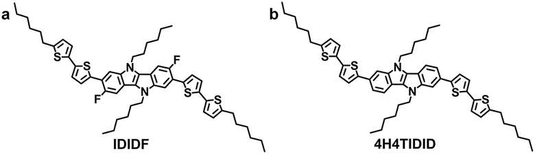 | ||
| Fig. 1 Molecular structure of IDIDF (a) and 4H4TIDID (b). | ||
In this regard, we have introduced a fluorine substituent into the IDID core (at the 3- and 8-positions) to enable an intramolecular interaction with the neighbouring thiophene through C–F⋯H, generating an extended planar π-conjugated backbone suitable for a p-type HTM (IDIDF in Fig. 1a) for PSCs. Its optoelectronic and electrochemical properties were characterized, together with single-crystal analysis. With respect to the hole mobility, the HOMO energy level, and the hole collection capability at the perovskite/HTM interface, IDIDF showed a better performance when compared with p,p-spiro-OMeTAD. As a result, we could demonstrate this new IDIDF compound as a best-performing class of HTMs for PSCs by achieving a high efficiency of 19% in this work.
Results and discussion
Fig. 1a depicts the molecular structure of IDIDF. As shown in Scheme 1, the synthetic procedure for the fluorinated IDID core, 2,7-dibromo-3,8-difluoro-5,10-dihydroindolo[3,2-b]indole (8), is essentially the same as that for 2,7-dibromo-5,10-dihydroindolo[3,2-b]indole, which was described in our previous report,7 but the additional bromination reaction of 5-fluoro-2-nitroaniline (1) is preceded. The obtained fluorinated IDID core was sequentially substituted with n-hexyl chains at two N-positions and a 5-hexyl-2,2′-bithiophene unit at the 2-, 7-position of the fluorinated IDID core by an SN2 reaction and Suzuki–Miyaura coupling reaction, respectively. The newly synthesized molecule, IDIDF, exhibited an acicular crystal habit, and is highly soluble in common organic solvents. The molecular structure was carefully characterized by 1H NMR, 13C NMR, elemental analysis, and mass analysis. The detailed synthetic procedure is described in the Experimental section.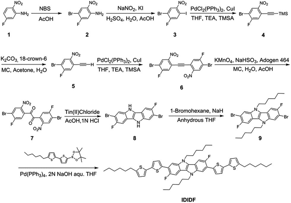 | ||
| Scheme 1 Synthetic route for IDIDF. | ||
Fig. 2 displays UV-vis absorption spectra of IDIDF in solution and in the film state. In the solution state, the π–π* transition of the absorption band was observed at 440 nm, whereas in the film state, the corresponding π–π* transition was found at 510 nm. Compared to that in solution, a large bathochromic shift of the absorption spectra in the film is clearly observed. In association with this shift, the solution-processed film, with good transparency, exhibited an apparently crystalline nature (see Fig. S1 in the ESI†), which is totally different from many amorphous HTMs, including spiro-OMeTAD for PSCs. As a result, this crystalline feature indicates a highly ordered structure of IDIDF molecules, most probably due to strong intermolecular interactions.
 | ||
| Fig. 2 UV-vis absorption spectra of IDIDF in a solution (tetrahydrofuran, 1 × 10⁻⁵ M) and film state. | ||
To fully elucidate the molecular conformation and packing motif of IDIDF in the solid state, single-crystal X-ray crystallography was performed (see Fig. 3, S2 and Table S1†). As for the molecular conformation, IDIDF exhibited an almost planar conformation with a torsion angle of 10.45° between the fluorinated IDID core and neighbouring thiophene, and a torsion angle of 0.98° between the two thiophenes. More importantly, the F⋯H distance between the fluorinated IDID core and a neighbouring thiophene was found to be 2.276 Å, which is less than the sum of the van der Waals radii of the fluorine and the hydrogen (=about 2.67 Å).8 Thus, the strong intramolecular interaction of C–F⋯H is one of the key factors reducing the distortion between the IDID core and the neighbouring thiophene, and enhancing the planarity of the elongated molecule. This may enable IDIDF to successfully build a single crystal. In contrast, for a molecule that was the same as IDIDF, except for F, 4H4TIDID, we could not obtain a single crystal for identifying the molecular packing, as in the previous study.7 With this planar structure, IDIDF crystallized in the P![[1 with combining macron]](https://www.rsc.org/images/entities/char_0031_0304.gif) space group of the triclinic system, with unit cell dimensions of a = 5.5351(1) Å, b = 13.7138(2) Å, c = 17.7912(3) Å, α = 68.191(1)°, β = 82.836(1)°, and γ = 80.889(1)°. As previously reported, p,p-spiro-OMeTAD exhibited a non-coplanar molecular structure and no direct short contact within the unit cell, thereby preventing π–π overlap.3j In contrast, as shown in Fig. 3c, IDIDF molecules stacked toward the a-axis with a slipped π-stacking motif, and the estimated π–π distance was 3.480 Å. Interestingly, one IDIDF has multiple short contacts with the neighbouring 8 molecules, and beside π–π contacts (3.362 Å for C–C), all of the four aliphatic side chains of IDIDF participate in intermolecular interactions with short contacts (2.388 Å and 2.312 Å for H–H and 2.985 Å for S–H, see Fig. 3d), giving rise to rigid and stable crystalline networks. Considering this tight π–π stacking and multiple contacts of IDIDF, we could expect efficient formation of hole-carrier transport channels in a pinhole-free crystalline film state (see Fig. S3†).9
space group of the triclinic system, with unit cell dimensions of a = 5.5351(1) Å, b = 13.7138(2) Å, c = 17.7912(3) Å, α = 68.191(1)°, β = 82.836(1)°, and γ = 80.889(1)°. As previously reported, p,p-spiro-OMeTAD exhibited a non-coplanar molecular structure and no direct short contact within the unit cell, thereby preventing π–π overlap.3j In contrast, as shown in Fig. 3c, IDIDF molecules stacked toward the a-axis with a slipped π-stacking motif, and the estimated π–π distance was 3.480 Å. Interestingly, one IDIDF has multiple short contacts with the neighbouring 8 molecules, and beside π–π contacts (3.362 Å for C–C), all of the four aliphatic side chains of IDIDF participate in intermolecular interactions with short contacts (2.388 Å and 2.312 Å for H–H and 2.985 Å for S–H, see Fig. 3d), giving rise to rigid and stable crystalline networks. Considering this tight π–π stacking and multiple contacts of IDIDF, we could expect efficient formation of hole-carrier transport channels in a pinhole-free crystalline film state (see Fig. S3†).9
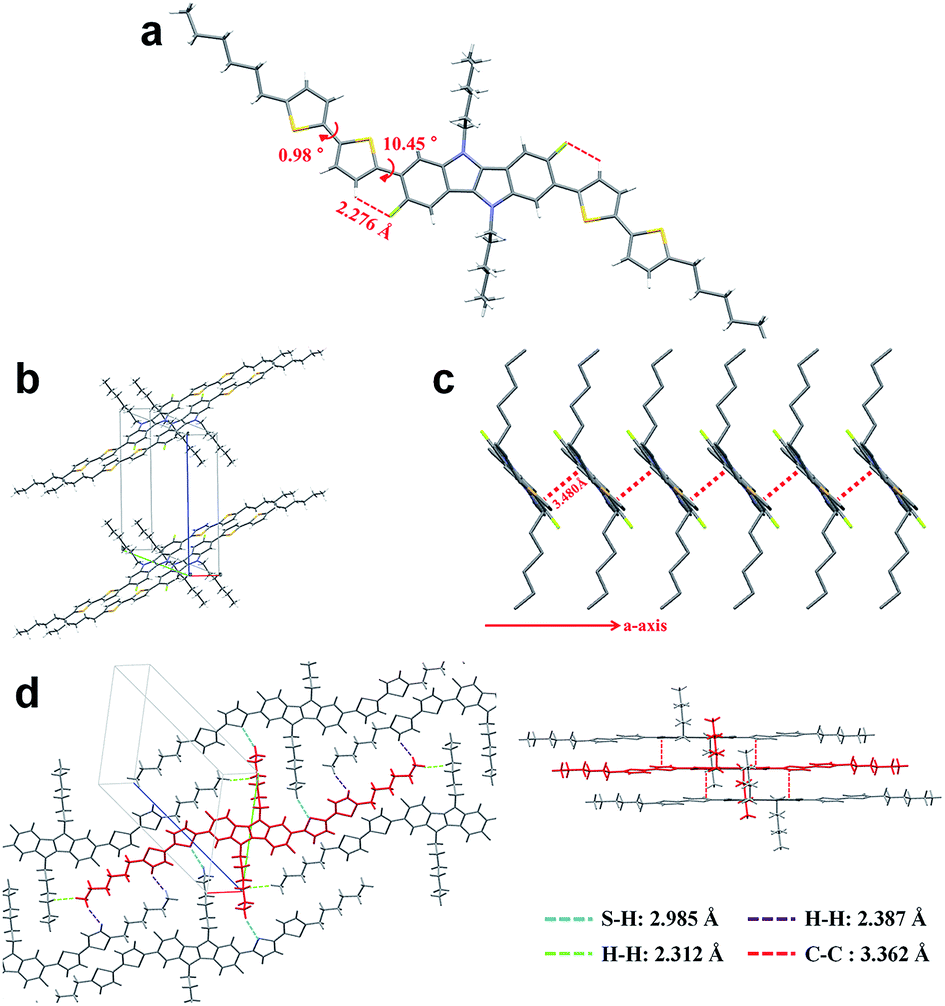 | ||
| Fig. 3 Single-crystal analysis of IDIDF. | ||
In order to obtain more insight into the charge transport properties of IDIDF, we carried out space-charge-limited currents (SCLCs) measurement according to a literature method.10 As shown in Fig. 4a, the hole mobility of each material was determined by fitting the J–V curves to the reported equation (see ESI†); the evaluated hole mobilities of p,p-spiro-OMeTAD and IDIDF are 2.17 × 10⁻⁴ cm2 V−1 s−1 and 1.69 × 10⁻³ cm2 V−1 s−1, respectively. The value obtained in this work for p,p-spiro-OMeTAD is similar to the data previously reported in the literature.11 Obviously, IDIDF shows a higher mobility than that of p,p-spiro-OMeTAD, which is attributed to a strong π–π interaction between the planar structures of the extended core, as revealed in Fig. 3.
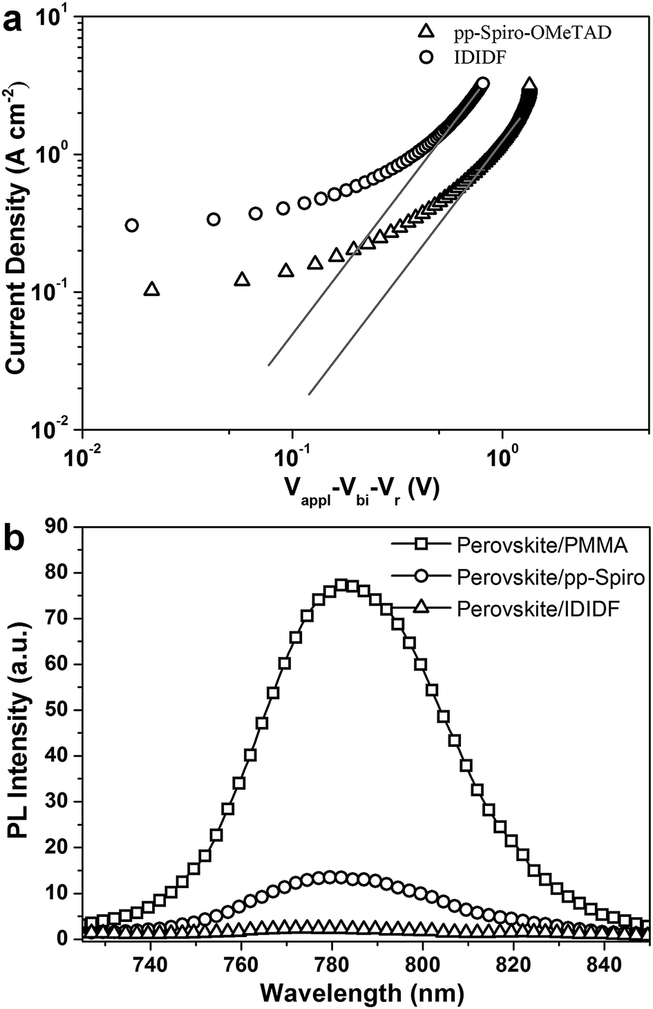 | ||
| Fig. 4 (a) The space-charge-limited-current (SCLC) of hole-only devices with the configuration of indium tin oxide (ITO)/poly(3,4-ethylenedioxythiophene)–polystyrene sulfonate (PEDOT:PSS)/p,p-spiro-OMeTAD or IDIDF (with Li-bis(trifluoromethanesulfonyl)imide (Li-TFSI) and 4-tert-butylpyridine (tBP) as additives)/Au. (b) PL emission spectra of perovskite/PMMA, perovskite/p,p-spiro-OMeTAD, and perovskite/IDIDF film under excitation at 670 nm. | ||
Photoluminescence (PL) quenching of the perovskite emission was examined to investigate the hole-accepting capability of the HTMs in bilayered film. A perovskite film employing a mixed perovskite of FAPbI3 and MAPbBr3 was prepared according to our previous publication.1c,e Upon excitation at 670 nm, a broad PL band of perovskite/PMMA film is observed to be centered at 780 nm. Perovskite/IDIDF film shows a much larger decrease in PL intensity, as compared with perovskite/p,p-spiro-OMeTAD film. This means that the charge transfer is more effective at the interface with IDIDF, exhibiting a better hole collection capability at the perovskite/IDIDF interface.3g,3f,12
With respect to the electrochemical properties, we recorded a cyclic voltammogram using the solid film, as shown in Fig. S4.† From this measurement, the HOMO energy levels were estimated to be −5.23 eV and −4.93 eV for IDIDF and p,p-spiro-OMeTAD, respectively. Their optical band gaps were found to be 2.30 eV and 2.94 eV from the edge of the absorption spectra, and thus the LUMO energy levels were evaluated to be −2.93 eV and −1.99 eV, respectively. In comparison to p,p-spiro-OMeTAD, the HOMO energy level of IDIDF was lower, but was still higher than the valence band (5.3 eV) of the perovskite, thereby providing sufficient driving force for hole transfer at the interface of the perovskite and IDIDF (see Fig. S5†). Importantly, however, this lower HOMO level is expected to lead to a higher open-circuit voltage (Voc) for IDIDF.
We fabricated FAPbI3-based PSC, which is based on a typical bilayered device configuration consisting of a fluorine-doped tin oxide (FTO) substrate/blocking layer, (bl)-TiO2/mp-TiO2/FAPbI3-based perovskite/HTM/Au. Through our solvent engineering technique, we prepared a dense and flat perovskite-absorbing layer on the mp-TiO2 scaffold, as shown in a cross-sectional SEM image of the whole device (see Fig. 5a). The subsequent deposition of IDIDF forms a ∼100 nm thick HTM layer, which is clearly distinguished from the perovskite layer and the Au electrode. Details are added in the ESI.†Fig. 5b shows a schematic energy-level diagram of the whole device. As explained above, IDIDF has appropriate HOMO and LUMO levels for facilitating hole extraction and blocking electron leakage, considering the valence and conduction bands of the perovskite in the device.
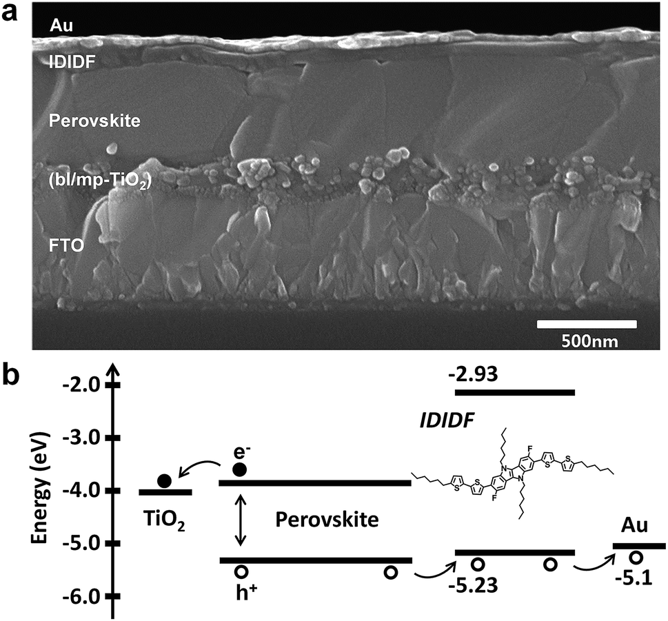 | ||
| Fig. 5 (a) Cross-sectional scanning electron microscopy (SEM) image of the device including FTO/bl-TiO2/mp-TiO2/perovskite/IDIDF/Au. (b) The schematic energy diagram of the corresponding device. | ||
Fig. 6a presents the average current density–voltage (J–V) curves for the best photovoltaic device fabricated using IDIDF under reverse and forward scans, resulting in an average PCE of 19.05%, together with Jsc = 23.55 mA cm−2, Voc = 1.045 V, and FF = 77.2%. The curve values obtained in both scan directions with 10 mV voltage steps and a delay time of 50 ms are averaged; the device shows a PCE of 19.8% for a reverse scan (from Voc to Jsc), and a PCE of 18.3% for a forward scan (from Jsc to Voc) (see Fig. S7 in ESI†). To obtain the exact efficiency of the resultant device, the steady-state photocurrent was monitored at a maximum power point of 0.88 V and the corresponding steady-state efficiency was estimated to be 18.8% (see Fig. 6b). This is close to the average PCE in the device. An external quantum efficiency (EQE) spectrum for the resultant device is shown in Fig. 6c. The integrated Jsc calculated from the EQE spectrum (∼23 mA cm−2) is similar to the measured Jsc. A high EQE of 80–88% in a broad range from 370 to 770 nm was found, which indicates efficient light harvesting originating from a light absorber of the FAPbI3-based perovskite, thereby contributing to a high Jsc. To unambiguously compare the performance with that of p,p-spiro-OMeTAD, we prepared devices using IDIDF and p,p-spiro-OMeTAD under the same conditions. As shown in Fig. 6d, the device fabricated using IDIDF exhibits a higher PCE than that using p,p-spiro-OMeTAD. Especially, as compared to other photovoltaic parameters, a relatively meaningful difference in Voc is found, which is supported by the fact that the HOMO energy level of IDIDF was lower than that of p,p-spiro-OMeTAD. Furthermore, as compared to p,p-spiro-OMeTAD, the higher hole mobility and higher hole collection capability of IDIDF must have facilitated hole extraction toward the Au, while minimizing carrier recombination, which is one of the factors leading to a higher FF and PCE. Finally, we tested the long-term stability of the device without encapsulation under a high humidity of 85%. For the p,p-spiro-OMeTAD-containing device, the performance decreased rapidly after exposure to moisture. When the device was exposed for 50 h, it became severely damaged. In contrast, the IDIDF-containing device showed a much better stability. The efficiency was maintained at almost 90% of its initial value after 50 h, although the HTM contained hygroscopic additives (Li-TFSI and tBP). It is noted that IDIDF molecules with highly crystalline packing act as a more effective moisture barrier than p,p-spiro-OMeTAD, with an amorphous glass nature (see Fig. S8†).
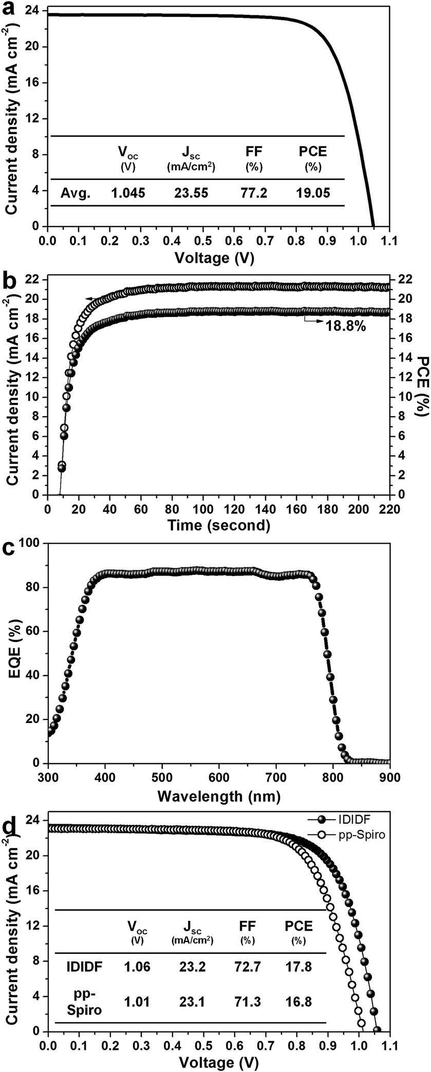 | ||
| Fig. 6 (a) Current density–voltage (J–V) curves of the best device (FTO/bl-TiO2/mp-TiO2/perovskite/IDIDF/Au). (b) The steady-state photocurrent and efficiency of the corresponding device at the maximum power point (0.88 V). (c) The corresponding external quantum efficiency (EQE) spectra. (d) A comparison of J–V curves of the devices fabricated using IDIDF and commercial p,p-spiro. Li-bis(trifluoromethanesulfonyl)imide (Li-TFSI) and 4-tert-butylpyridine (tBP) are used as additives in this work. Statistical power conversion efficiency distributions of 32 PSC devices for IDIDF and p,p-spiro-OMeTAD are depicted in Fig. S6.† | ||
Conclusion
We synthesized a fluorinated indoloindole derivative as a high-performance crystalline HTM for perovskite solar cells. A planar π-conjugated backbone linked with a flexible alkyl chain enabled the formation of a molecular arrangement stacked by strong π–π interactions, which was revealed in single-crystal analysis. In this regard, IDIDF in the film state showed a higher mobility than that of p,p-spiro-OMeTAD. PL quenching occurred more effectively at the perovskite/IDIDF interface, compared to that at the perovskite/p,p-spiro-OMeTAD. From CV measurement, proper HOMO and LUMO energy levels for IDIDF were found to be suitable for a HTM. As a result, the device fabricated using IDIDF showed a better performance as compared to p,p-spiro-OMeTAD, exhibiting a best PCE of 19%. It was thus shown that a planar IDID core-based crystalline HTM is a promising candidate for highly efficient perovskite solar cells.Experimental
Synthetic procedures
IDIDF was synthesized according to the procedure shown in Scheme 1. Unless stated otherwise, all reagents were purchased at Sigma Aldrich, TCI, and Alfa Aesar.![[thin space (1/6-em)]](https://www.rsc.org/images/entities/char_2009.gif) :9, v/v) to afford 4 as a dark brown oil (4.85 g, yield 75.79%). 1H-NMR (300 MHz, CDCl3, δ): 8.31 (d, J = 6.24 Hz, 1H), 7.38 (d, J = 8.19 Hz, 1H), 0.28 (s, 9H).
:3, v/v) to afford 5 as a brown powder (2.79 g, yield 75.57%). 1H-NMR (300 MHz, CDCl3, δ): 8.36 (d, J = 6.24 Hz, 1H), 7.43 (d, J = 8.04 Hz, 1H), 3.64 (s, 1H).
:2 v/v) and the resulting solid was washed with chloroform (100 mL × 1) to afford 8 as a light brown solid (1.23 g, yield 82.10%). 1H-NMR (300 MHz, acetone-d6, δ): 10.47 (s, 2H), 7.84 (d, J = 5.88 Hz, 2H), 7.67 (d, J = 9.36 Hz, 2H).
:4, v/v) and recrystallization (EA) to afford 9 as a white crystalline solid (410 mg, yield 75.94%). 1H-NMR (300 MHz, THF-d8, δ): 7.94 (d, J = 5.76 Hz, 2H), 7.84 (d, J = 9.45 Hz, 2H), 4.62 (t, J = 7.08 Hz, 4H), 1.94 (m, J = 7.23 Hz, 4H), 1.45–1.19 (m, 12H), 0.81 (t, J = 7.11 Hz, 6H).
:4, v/v) and recrystallization (EA) to afford IDIDF as orange crystals (760 mg, yield 73.23%). 1H-NMR (500 MHz, tetrahydrofuran-d8, δ): 7.78 (d, J = 6 Hz, 2H), 7.69 (d, J = 12 Hz, 2H), 7.46 (d, J = 3.5 Hz, 2H), 7.16 (d, J = 4 Hz, 2H), 7.07 (d, J = 3.5 Hz, 2H), 6.74 (d, J = 3.5 Hz, 2H), 4.58 (t, J = 7 Hz, 4H), 2.82 (t, J = 7.5 Hz, 4H), 1.98–1.93 (m, 4H), 1.71–1.69 (m, 4H), 1.45–1.27 (m, 24H), 0.91 (t, J = 7 Hz, 6H), 0.85 (t, J = 7 Hz, 6H). 13C NMR (500 MHz, tetrahydrofuran-d8, δ): 155.73, 153.83, 146.13, 139.27, 138.48, 138.45, 138.25, 138.22, 135.95, 129.09, 127.24, 127.20, 126.04, 124.37, 124.14, 118.07, 117.94, 114.01, 113.92, 109.36, 109.33, 104.99, 104.78, 45.98, 32.74, 31.38, 31.01, 29.84, 27.70, 23.64, 23.60, 14.59, 14.52, HRMS (FAB, m/z): calcd for C54H62F2N2S4: 906.39, found: 906.392. Elem. anal. calcd for C54H62F2N2S4: C 71.48, H 7.11, F 4.19, N 3.09, S 14.13; found: C 71.14, H 7.22, N 3.08, S 13.94.
:9, v/v) to afford 4 as a dark brown oil (4.85 g, yield 75.79%). 1H-NMR (300 MHz, CDCl3, δ): 8.31 (d, J = 6.24 Hz, 1H), 7.38 (d, J = 8.19 Hz, 1H), 0.28 (s, 9H).
:3, v/v) to afford 5 as a brown powder (2.79 g, yield 75.57%). 1H-NMR (300 MHz, CDCl3, δ): 8.36 (d, J = 6.24 Hz, 1H), 7.43 (d, J = 8.04 Hz, 1H), 3.64 (s, 1H).
:2 v/v) and the resulting solid was washed with chloroform (100 mL × 1) to afford 8 as a light brown solid (1.23 g, yield 82.10%). 1H-NMR (300 MHz, acetone-d6, δ): 10.47 (s, 2H), 7.84 (d, J = 5.88 Hz, 2H), 7.67 (d, J = 9.36 Hz, 2H).
:4, v/v) and recrystallization (EA) to afford 9 as a white crystalline solid (410 mg, yield 75.94%). 1H-NMR (300 MHz, THF-d8, δ): 7.94 (d, J = 5.76 Hz, 2H), 7.84 (d, J = 9.45 Hz, 2H), 4.62 (t, J = 7.08 Hz, 4H), 1.94 (m, J = 7.23 Hz, 4H), 1.45–1.19 (m, 12H), 0.81 (t, J = 7.11 Hz, 6H).
:4, v/v) and recrystallization (EA) to afford IDIDF as orange crystals (760 mg, yield 73.23%). 1H-NMR (500 MHz, tetrahydrofuran-d8, δ): 7.78 (d, J = 6 Hz, 2H), 7.69 (d, J = 12 Hz, 2H), 7.46 (d, J = 3.5 Hz, 2H), 7.16 (d, J = 4 Hz, 2H), 7.07 (d, J = 3.5 Hz, 2H), 6.74 (d, J = 3.5 Hz, 2H), 4.58 (t, J = 7 Hz, 4H), 2.82 (t, J = 7.5 Hz, 4H), 1.98–1.93 (m, 4H), 1.71–1.69 (m, 4H), 1.45–1.27 (m, 24H), 0.91 (t, J = 7 Hz, 6H), 0.85 (t, J = 7 Hz, 6H). 13C NMR (500 MHz, tetrahydrofuran-d8, δ): 155.73, 153.83, 146.13, 139.27, 138.48, 138.45, 138.25, 138.22, 135.95, 129.09, 127.24, 127.20, 126.04, 124.37, 124.14, 118.07, 117.94, 114.01, 113.92, 109.36, 109.33, 104.99, 104.78, 45.98, 32.74, 31.38, 31.01, 29.84, 27.70, 23.64, 23.60, 14.59, 14.52, HRMS (FAB, m/z): calcd for C54H62F2N2S4: 906.39, found: 906.392. Elem. anal. calcd for C54H62F2N2S4: C 71.48, H 7.11, F 4.19, N 3.09, S 14.13; found: C 71.14, H 7.22, N 3.08, S 13.94.
Device fabrication and measurement
The F-doped SnO2 (FTO, Pilkington, TEC8) substrate was cleaned in an ultrasonic bath containing detergents for 30 min, and then a dense blocking layer of TiO2 (60 nm, bl-TiO2) was deposited onto the FTO by spray pyrolysis, using a 20 mM titanium diisopropoxide bis(acetylacetonate) solution (Aldrich) at 450 °C. A 100 nm thin mesoporous (mp)-TiO2 was spin-coated on top of the bl-TiO2/FTO substrate at 1000 rpm for 50 s, using home-made TiO2 (∼50 nm in particle size) pastes. The pristine paste had been diluted in 2-methoxyethanol (1 g/5 mL), and calcinated at 500 °C for 1 h in air, which led to a thickness of about 100 nm. The (FAPbI3)0.92(MAPbBr3)0.08 perovskite solutions with a small excess of PbI2 were then coated onto the mp-TiO2/bl-TiO2/FTO substrate heated to 50 °C by two consecutive spin-coating steps, at 1000 and 5000 rpm for 5 s and 10 s, respectively. During the second spin-coating step, 1 mL ethyl ether was poured onto the substrate. The 1.05 M solution for (FAPbI3)0.92(MAPbBr3)0.08 perovskite was obtained by dissolving NH2CH![[double bond, length as m-dash]](https://www.rsc.org/images/entities/char_e001.gif) NH2I (=FAI) and CH3NH3Br (=MABr) with PbI2 and PbBr2 in N,N-dimethylformamide (=DMF) and dimethylsulfoxide (=DMSO) = (6:1 v/v). Then, the perovskite-deposited substrate was dried on a hot plate at 150 °C for 10 min. A p,p-spiro-OMeTAD/chlorobenzene (30 mg/1 mL) solution with 21.5 μL Li-bis(trifluoromethanesulfonyl) imide (Li-TFSI)/acetonitrile (170 mg/1 mL) and 21.5 μL 4-tert-butylpyridine (TBP)/acetonitrile (1 mL/1 mL) as additives was spin-coated on the (FAPbI3)0.92(MAPbBr3)0.08/mp-TiO2/bl-TiO2/FTO substrate at 3000 rpm for 30 s. By following the same procedure, IDIDF was deposited. Finally, the Au counter electrode was deposited by thermal evaporation. The active area of this electrode was fixed at 0.16 cm2. The cross-sections of the perovskite films were investigated using FE-SEM (Tescan Mira 3 LMU FEG). The absorption spectra were obtained using a UV-visible spectrophotometer (Shimadzu UV 2550) in the wavelength range 300 nm to 850 nm. The photovoltaic properties of the devices were measured using a solar simulator (Newport, Oriel Class A, 91195 A) with a source meter (Keithley 2420) at AM 1.5 G 100 mA cm−2 of illumination, and a calibrated Si-reference cell certificated by NREL. The J–V curves of all the devices were measured by masking the active area using a metal mask with an area of 0.0955 cm2. The external quantum efficiency (EQE) was measured using a power source (Newport 300 W xenon lamp, 66920) with a monochromator (Newport Cornerstone 260) and a multimeter (Keithley 2001). The ionization energy for the mixed perovskite film on fused silica was measured using photoelectron spectroscopy (Riken Keiki AC-2).
NH2I (=FAI) and CH3NH3Br (=MABr) with PbI2 and PbBr2 in N,N-dimethylformamide (=DMF) and dimethylsulfoxide (=DMSO) = (6:1 v/v). Then, the perovskite-deposited substrate was dried on a hot plate at 150 °C for 10 min. A p,p-spiro-OMeTAD/chlorobenzene (30 mg/1 mL) solution with 21.5 μL Li-bis(trifluoromethanesulfonyl) imide (Li-TFSI)/acetonitrile (170 mg/1 mL) and 21.5 μL 4-tert-butylpyridine (TBP)/acetonitrile (1 mL/1 mL) as additives was spin-coated on the (FAPbI3)0.92(MAPbBr3)0.08/mp-TiO2/bl-TiO2/FTO substrate at 3000 rpm for 30 s. By following the same procedure, IDIDF was deposited. Finally, the Au counter electrode was deposited by thermal evaporation. The active area of this electrode was fixed at 0.16 cm2. The cross-sections of the perovskite films were investigated using FE-SEM (Tescan Mira 3 LMU FEG). The absorption spectra were obtained using a UV-visible spectrophotometer (Shimadzu UV 2550) in the wavelength range 300 nm to 850 nm. The photovoltaic properties of the devices were measured using a solar simulator (Newport, Oriel Class A, 91195 A) with a source meter (Keithley 2420) at AM 1.5 G 100 mA cm−2 of illumination, and a calibrated Si-reference cell certificated by NREL. The J–V curves of all the devices were measured by masking the active area using a metal mask with an area of 0.0955 cm2. The external quantum efficiency (EQE) was measured using a power source (Newport 300 W xenon lamp, 66920) with a monochromator (Newport Cornerstone 260) and a multimeter (Keithley 2001). The ionization energy for the mixed perovskite film on fused silica was measured using photoelectron spectroscopy (Riken Keiki AC-2).
Acknowledgements
This work was supported by the National Research Foundation of Korea (NRF) through a grant funded by the Korean Government (MSIP; No. 2009-0081571[RIAM0417-20150013]) and the Global Frontier R&D Program at the Center for Multiscale Energy Systems funded by the National Research Foundation under the Ministry of Science, ICT & Future Planning, Korea (2012M3A6A7055540) (Global Frontier R&D Program on Center for Multiscale Energy System) and NRF-2015M1A2A2056542. This work was also supported by a grant from the Korea Research Institute of Chemical Technology (KRICT), Republic of Korea (KK1602-A01). N. J. Jeon also acknowledges support by the Basic Science Research Program through the NRF, funded by the Ministry of Education (NRF-2015R1A6A3A04058164).Notes and references
- (a) A. Kojima, K. Teshima, Y. Shirai and T. Miyasaka, J. Am. Chem. Soc., 2009, 131, 6050 CrossRef CAS PubMed; (b) P. Gao, M. Grätzel and M. K. Nazeeruddin, Energy Environ. Sci., 2014, 7, 2448 RSC; (c) N. J. Jeon, J. H. Noh, W. S. Yang, Y. C. Kim, S. Ryu, J. Seo and S. I. Seok, Nature, 2015, 517, 476 CrossRef CAS PubMed; (d) W. S. Yang, J. H. Noh, N. J. Jeon, Y. C. Kim, S. Ryu, J. Seo and S. I. Seok, Science, 2015, 348, 1234 CrossRef CAS PubMed; (e) Y. C. Kim, J. H. Noh, N. J. Jeon, W. S. Yang, J. Seo, J. S. Yun, A. Ho-Baillie, S. Huang, M. A. Green, J. Seidel, T. K. Ahn and S. I. Seok, Adv. Energy Mater., 2016, 6, 1502104 CrossRef; (f) K. Domanski, J.-P. Correa-Baena, N. Mine, M. K. Nazeeruddin, A. Abate, M. Saliba, W. Tress, A. Hagfeldt and M. Grätzel, ACS Nano, 2016, 10, 6306 CrossRef CAS PubMed; (g) M. Saliba, T. Matsui, J.-Y. Seo, K. Domanski, J. P. Correa-Baena, M. K. Nazeeruddin, S. M. Zakeeruddin, W. Tress, A. Abate, A. Hagfeldt and M. Grätzel, Energy Environ. Sci., 2016, 9, 1989 RSC; (h) T. Malinauskas, M. Saliba, T. Matsui, M. Daskeviciene, S. Urnikaite, P. Gratia, R. Send, H. Wonneberger, I. Bruder, M. Graetzel, V. Getautis and M. K. Nazeeruddin, Energy Environ. Sci., 2016, 9, 1681 RSC; (i) http://www.nrel.gov/ncpv/images/efficiency_chart.jpg .
- (a) F. Matteocci, S. Razza, F. D. Giacomo, S. Casaluci, G. Mincuzzi, T. M. Brown, A. D. 'Epifanio, S. Licoccia and A. D. Carlo, Phys. Chem. Chem. Phys., 2014, 16, 3918 RSC; (b) Y. Rong, L. Liu, A. Mei, X. Li and H. Han, Adv. Energy Mater., 2015, 5, 1501066 CrossRef.
- (a) H. Li, K. Fu, A. Hagfeldt, M. Grätzel, S. G. Mhaisalkar and A. C. Grims-dale, Angew. Chem., Int. Ed., 2014, 53, 4085 CrossRef CAS PubMed; (b) T. Krishnamoorthy, F. Kunwu, P. P. Boix, H. Li, T. M. Koh, W. L. Leong, S. Powar, A. Grimsdale, M. Grätzel, N. Mathews and S. G. Mhaisalkar, J. Mater. Chem. A, 2014, 2, 6305 RSC; (c) P. Qin, S. Paek, M. I. Dar, N. Pellet, J. Ko, M. Grätzel and M. K. Nazeeruddin, J. Am. Chem. Soc., 2014, 136, 8516 CrossRef CAS PubMed; (d) N. J. Jeon, J. Lee, J. H. Noh, M. K. Nazeeruddin, M. Grätzel and S. I. Seok, J. Am. Chem. Soc., 2013, 135, 19087 CrossRef CAS PubMed; (e) A. Krishna, D. Sabba, H. R. Li, J. Yin, P. P. Boix, C. Soci, S. G. Mhaisalkar and A. C. Grimsdale, Chem. Sci., 2014, 5, 2702 RSC; (f) S. Paek, I. Zimmermann, P. Gao, K. Rakstys, G. Grancini, M. K. Nazeeruddin, M. A. Rub, S. A. Kosa, K. A. Alamry and A. M. Asiri, Chem. Sci., 2016, 7, 6068 RSC; (g) J. Zhang, Y. Hua, B. Xu, L. Yang, P. Liu, M. B. Johansson, N. Vlachopoulos, L. Kloo, G. Boschloo, E. M. J. Johansson, L. Sun and A. Hagfeldt, Adv. Energy Mater., 2016, 1601062, DOI:10.1002/aenm.201601062; (h) S. Paek, M. A. Rub, H. Choi, S. A. Kosa, K. A. Alamry, J. W. Cho, P. Gao, J. Ko, A. M. Asiri and M. K. Nazeeruddin, Nanoscale, 2016, 8, 6335 RSC; (i) D. Bi, A. Mishra, P. Gao, M. Franckevičius, C. Steck, S. M. Zakeeruddin, M. K. Nazeeruddin, P. Bäuerle, M. Grätzel and A. Hagfeldt, ChemSusChem, 2016, 9, 433 CrossRef CAS PubMed; (j) P. Ganesan, K. Fu, P. Gao, I. Raabe, K. Schenk, R. Scopelliti, J. Luo, L. H. Wong, M. Grätzel and M. K. Nazeeruddin, Energy Environ. Sci., 2015, 8, 1986 RSC.
- (a) N. J. Jeon, H. G. Lee, Y. C. Kim, J. Seo, J. H. Noh, J. Lee and S. I. Seok, J. Am. Chem. Soc., 2014, 136, 7837 CrossRef CAS PubMed; (b) J. Seo, N. J. Jeon, W. S. Yang, H.-W. Shin, T. K. Ahn, J. Lee, J. H. Noh and S. I. Seok, Adv. Energy Mater., 2015, 5, 1501320 CrossRef; (c) M. Saliba, S. Orlandi, T. Matsui, S. Aghazada, M. Cavazzini, J.-P. Correa-Baena, P. Gao, R. Scopelliti, E. Mosconi, K.-H. Dahmen, F. D. Andgelis, A. Abate, A. Hagfeldt, G. Pozzi, M. Grätzel and M. K. Nazeeruddin, Nat. Energy, 15017, DOI:10.1038/nenergy.2015.17.
- (a) H. Wang, A. D. Sheikh, Q. Feng, F. Li, Y. Chen, W. Yu, E. Alarousu, C. Ma, M. A. Haque, D. Shi, Z.-S. Wang, O. F. Mohammed, O. M. Bakr and T. Wu, ACS Photonics, 2015, 2, 849 CrossRef CAS; (b) I. Lim, E.-K. Kim, S. A. Patil, D. Y. Ahn, W. Lee, N. K. Shrestha, J. K. Lee, W. K. Seok, C.-G. Cho and S.-W. Han, RSC Adv., 2015, 5, 55321 RSC; (c) K. Rakstys, A. Abate, M. I. Dar, P. Gao, V. Jankauskas, G. Jacopin, E. Kamarauskas, S. Kazim, S. Ahmad, M. Grätzel and M. K. Nazeeruddin, J. Am. Chem. Soc., 2015, 137, 16172 CrossRef CAS PubMed.
- (a) Y. Jin, K. Kim, S. Song, J. Kim, J. Kim, S. H. Park, K. Lee and H. Shu, Bull. Korean Chem. Soc., 2006, 27, 1043 CrossRef CAS; (b) L. Qiu, C. Yu, N. Zhao, W. Chen, Y. Guo, X. Wan, R. Yang and Y. Liu, Chem. Commun., 2012, 48, 12225 RSC; (c) Y.-Y. Lai, J.-M. Yeh, C.-E. Tsai and Y.-J. Cheng, Eur. J. Org. Chem., 2013, 5076 CrossRef CAS.
- I. Cho, S. K. Park, B. Kang, J. W. Chung, J. H. Kim, K. Cho and S. Y. Park, Adv. Funct. Mater., 2016, 26, 2966 CrossRef CAS.
- K. Reichenbächer, H. I. Süss and J. Hulliger, Chem. Soc. Rev., 2005, 34, 22 RSC.
- G. Gong, N. Zhao, D. Ni, J. Chen, Y. Shen, M. Wang and G. Tu, J. Mater. Chem. A, 2016, 4, 3661 CAS.
- O. K. Kwon, M. A. Uddin, J. H. Park, S. K. Park, T. L. Nguyen, H. Y. Woo and S. Y. Park, Adv. Mater., 2016, 28, 910 CrossRef CAS PubMed.
- S. S. Reddy, K. Gunasekar, J. H. Heo, S. H. Im, C. S. Kim, D.-H. Kim, J. H. Moon, J. Y. Lee, M. Song and S.-H. Jin, Adv. Mater., 2016, 28, 686 CrossRef CAS PubMed.
- (a) N. Arora, S. Orlandi, M. I. Dar, S. Aghazada, G. Jacopin, M. Cavazzini, E. Mosconi, P. Gratia, F. D. Angelis, G. Pozzi, M. Grätzel and M. K. Nazeeruddin, ACS Energy Letters, 2016, 1, 107 CrossRef CAS; (b) S. D. Stranks, G. E. Eperon, G. Grancini, C. Menelaou, M. J. P. Alcocer, T. Leijtens, L. M. Herz, A. Petrozza and H. J. Snaith, Science, 2013, 342, 341 CrossRef CAS PubMed; (c) S. Sun, T. Salim, N. Mathews, M. Duchamp, C. Boothroyd, G. Xing, T. C. Sum and Y. M. Lam, Energy Environ. Sci., 2014, 7, 399 RSC; (d) Y. Li, L. Meng, Y. Yang, G. Xu, Z. Hong, Q. Chen, J. You, G. Li, Y. Yang and Y. Li, Nat. Commun., 2016, 7, 10214 CrossRef CAS PubMed.
Footnotes |
| † Electronic supplementary information (ESI) available: Experimental details and additional supplementary figures. CCDC 1453030. For ESI and crystallographic data in CIF or other electronic format see DOI: 10.1039/c6sc02832b |
| ‡ These authors contributed equally to this work. |
| This journal is © The Royal Society of Chemistry 2017 |