
 Open Access Article
 This Open Access Article is licensed under a Creative Commons Attribution-Non Commercial 3.0 Unported Licence
Enhancement of light-emitting properties by simultaneously patterning and controlling molecular alignment in polyfluorene thin films†
X. H. Lia,
X. Z. Shena,
X. Gaob and
Y. Y. Weng *a
*a
aCentre for Soft Condensed Matter Physics and Interdisciplinary Research, College of Physics, Optoelectronics and Energy, Soochow University, Suzhou, 215006, China. E-mail: wengyuyan@suda.edu.cn
bInstitute of Functional Nano & Soft Materials (FUNSOM), Collaborative Innovation Centre of Suzhou Nano Science & Technology, Soochow University, Suzhou 215006, China
First published on 11th December 2017
Abstract
Soft nano-imprinting lithography is used to fabricate PFO nanogratings. On the one hand, soft nano-imprinting lithography has been well explored to create nanostructures and induce molecular orientation in conjugated polymer thin films because of its limited cost, high throughput, and small feature size. On the other hand, the pure α-conformation PFO nanogratings with highly ordered molecular chains can be achieved with graphoepitaxial alignment without any molecular chain degradation. Hence, herein, we demonstrated that large-area PFO (poly(9,9-dioctylfluorene)) nanogratings could be fabricated by this effective way with high accuracy of patterning and chain alignment controllability. The molecular chain alignment degree can be tuned due to entropic and geometrical reasons; this has been verified by polarized absorption and GIWAXD (grazing incidence wide angle X-ray diffraction). Moreover, both the optical and electrical pumping properties have been characterized. In addition, not only optimized polarizability was observed at the most oriented situation, but also 20% more light was extracted from this PLED device.
Introduction
With the development of LEDs, cold cathode fluorescent lamps have been significantly replaced because of their power consumption, heat, brightness, and lifetime. LED has been widely used in laptops, cell phones, and other flat panel displays. Moreover, PLED have dominated almost half the market of the LED on display backlights as they are flat, thin, and flexible. A polarized light source is more preferred for PLED display as a traditional absorbing sheet polarizer is not very efficient. More than 50% of light would remain unused when unpolarized light is passed through a polarizer to obtain polarized light.1–3 Therefore, many approaches, such as rubbing,4 stretching,5 and friction-transfer,6–8 have been developed to induce chain alignment in thin films. An additional polymer layer, such as a rubbed polyimide film9 or a photo-induced azobenzene film, has also been introduced into these approaches.10,11 Most of these assisting thin layers are good insulators, whose thicknesses do not exceed tens of nanometers in the traditional PLED 5-layer structure. Hence, the molecular chain alignment without any assisting layers would be more appreciated. Considering this, a number of studies have been focused on confinement-induced molecular chain alignment during the nanoimprint process.12–14Because of high luminescence efficiency, relatively high charge carrier mobility, and excellent thermal stability, PFO is a good candidate for a blue-emitting active layer on PLED devices,15–17 and the alignment of these molecular chains can result in the emission of polarized blue light.18–20 As a rod-like conjugated polymer, the PFO molecular chain arrangement can be affected by graphoepitaxial alignment and nanoconfinement in the cavities of the nanoimprinting templates.13,21,22 By efficiently tuning the PFO molecular chain alignment degree in the active layer, polarizability improvement can be realized.
On the other hand, it has been reported that photonic crystals formed on the surface or in the active layer can be used to extract more light from the PLED devices.23–25 However, it is difficult to simultaneously introduce photonic crystal structures and induce chain alignment in one active layer of PLED. Herein, we demonstrated that both achievements could be directly realized on nanoembossing PFO thin films. In this study, one-step fabrication of the active layer of PLED has been demonstrated, which can spontaneously realize high emission intensity and polarizability.
Results and discussion
PFO (poly(9,9-dioctylfluorene)) was purchased from American dye source company and used as received, and the molecular weight of PFO (Mw = 68![[thin space (1/6-em)]](https://www.rsc.org/images/entities/char_2009.gif) 000 g mol−1, PDI = 4.3) is supported by the American dye source company. The PFO powder was dissolved in toluene, and the PFO thin films were prepared by spin-coating. The substrates used were quartz glass and silicon wafer, cleaned in freshly prepared piranha solution (H2O2 (27%) and H2SO4 (98%) 1:3). The film thickness depended on both the spin speed and the solution concentration. To control the thickness of the spin-coated film in the range between 25 nm and 90 nm, solution concentration in the range from 10 mg ml−1 to 20 mg ml−1 was chosen, and spin speeds were between 2000 rpm and 4000 rpm. The α-conformation thin film achieved by thermal annealing at 180 °C for 5 minutes was slowly cooled down to 135 °C, kept for 10 minutes at this temperature, and then cooled down to room temperature. These spin-coated films were transferred to a nanoimprinter (Obducat, Eitre 3) and covered with PDMS (polydimethylsiloxane) template replicated from the polymethylmethacrylate (PMMA) template by E-beam lithography. The PDMS templates were pressed against the films under pressure (60 bar) at 180 °C for 5 min to ensure that nanotrenches in the template were fully immersed in the PFO layer; the templates were then cooled down to 135 °C, held at this temperature for 10 min, and then slowly cooled down to room temperature (30 °C). Before releasing the pressure, the stacks were evacuated to solidify the PFO nanogratings. The soft-NIL process is schematically shown in Fig. 1(a). The template used for this process was PDMS soft template considering its fabrication cost. The area of the PDMS stamp was about 64 mm2 and height was about 100 nm with 300 nm line-width and duty cycle around 0.5, as shown in Fig. sp1.† As shown in the AFM image in Fig. 1(d), the 300 nm line-width PFO nanogratings with different initial layer thicknesses were reproduced on the silicon wafer. By carefully tuning the initial PFO layer thickness, different filling quantities in the same PDMS stamp could be easily realized during the soft NIL process. Hence, a series of different residual and protrusion layer thicknesses could be achieved after the NIL process. A series of the protrusion layer and residual layer thicknesses are shown in Table 1, characterized by SEM shown in Fig. sp2.† Since the nano-trenches on the PDMS template were about 100 nm deep, the protrusions on the PFO nanograting could not exceed 100 nm in height, as shown in the AFM images in Fig. sp3.†
000 g mol−1, PDI = 4.3) is supported by the American dye source company. The PFO powder was dissolved in toluene, and the PFO thin films were prepared by spin-coating. The substrates used were quartz glass and silicon wafer, cleaned in freshly prepared piranha solution (H2O2 (27%) and H2SO4 (98%) 1:3). The film thickness depended on both the spin speed and the solution concentration. To control the thickness of the spin-coated film in the range between 25 nm and 90 nm, solution concentration in the range from 10 mg ml−1 to 20 mg ml−1 was chosen, and spin speeds were between 2000 rpm and 4000 rpm. The α-conformation thin film achieved by thermal annealing at 180 °C for 5 minutes was slowly cooled down to 135 °C, kept for 10 minutes at this temperature, and then cooled down to room temperature. These spin-coated films were transferred to a nanoimprinter (Obducat, Eitre 3) and covered with PDMS (polydimethylsiloxane) template replicated from the polymethylmethacrylate (PMMA) template by E-beam lithography. The PDMS templates were pressed against the films under pressure (60 bar) at 180 °C for 5 min to ensure that nanotrenches in the template were fully immersed in the PFO layer; the templates were then cooled down to 135 °C, held at this temperature for 10 min, and then slowly cooled down to room temperature (30 °C). Before releasing the pressure, the stacks were evacuated to solidify the PFO nanogratings. The soft-NIL process is schematically shown in Fig. 1(a). The template used for this process was PDMS soft template considering its fabrication cost. The area of the PDMS stamp was about 64 mm2 and height was about 100 nm with 300 nm line-width and duty cycle around 0.5, as shown in Fig. sp1.† As shown in the AFM image in Fig. 1(d), the 300 nm line-width PFO nanogratings with different initial layer thicknesses were reproduced on the silicon wafer. By carefully tuning the initial PFO layer thickness, different filling quantities in the same PDMS stamp could be easily realized during the soft NIL process. Hence, a series of different residual and protrusion layer thicknesses could be achieved after the NIL process. A series of the protrusion layer and residual layer thicknesses are shown in Table 1, characterized by SEM shown in Fig. sp2.† Since the nano-trenches on the PDMS template were about 100 nm deep, the protrusions on the PFO nanograting could not exceed 100 nm in height, as shown in the AFM images in Fig. sp3.†
 | ||
| Fig. 1 One-step fabrication of the PFO nanograting. (a–c) Nanoimprinting process of the PFO nanograting. (d) AFM image of the PFO nanograting. | ||
| Initial film thickness | Residual layer thickness (hr) | Protrusion layer thickness (hp) |
|---|---|---|
| 25 nm | <10 nm | 40 nm |
| 30 nm | <10 nm | 50 nm |
| 50 nm | <10 nm | 90 nm |
| 65 nm | ≈10 nm | 90 nm |
| 75 nm | 28 nm | 90 nm |
| 90 nm | 49 nm | 90 nm |
As the AFM and SEM analysis is limited to visualizing the surface morphology, GIWAXD measurement was used to analyse the orientation of the α-conformation PFO gratings, whose incident azimuth angle was fixed at about 0.18° to probe the orientation. Taking the nanogratings with 60 nm-thickness as an example, we defined the diffraction vectors qxy and qz pointing along and normal to the substrate plane, respectively, and the lattice parameters of PFO in the orthorhombic unit were a = 2.56 nm, b = 2.38 nm, c = 3.32 nm.26,27 The GIWAXD patterns are shown in Fig. 2(a) and (b); the incident X-ray beam is perpendicular or parallel to the long axis of nanogratings. In the qz direction, whether the incident X-ray beam is perpendicular or parallel to the nanogratings, the peaks at qz = 4.91 nm−1 corresponding to the (200) diffraction planes indicate the edge-on chain orientation with respect to the substrate surface. On the other hand, in the qxy direction, the peaks at qxy = 15.14 nm−1 corresponding to the (008) diffraction planes with the incident X-ray beam perpendicular to the nanogratings and the peaks at qxy = 10.74 nm−1 and 16.11 nm−1 corresponding to the (040) and (060) diffraction planes with the incident X-ray beam parallel to the nanogratings indicate that the polymer backbone is aligned along the long axis of nanogratings.
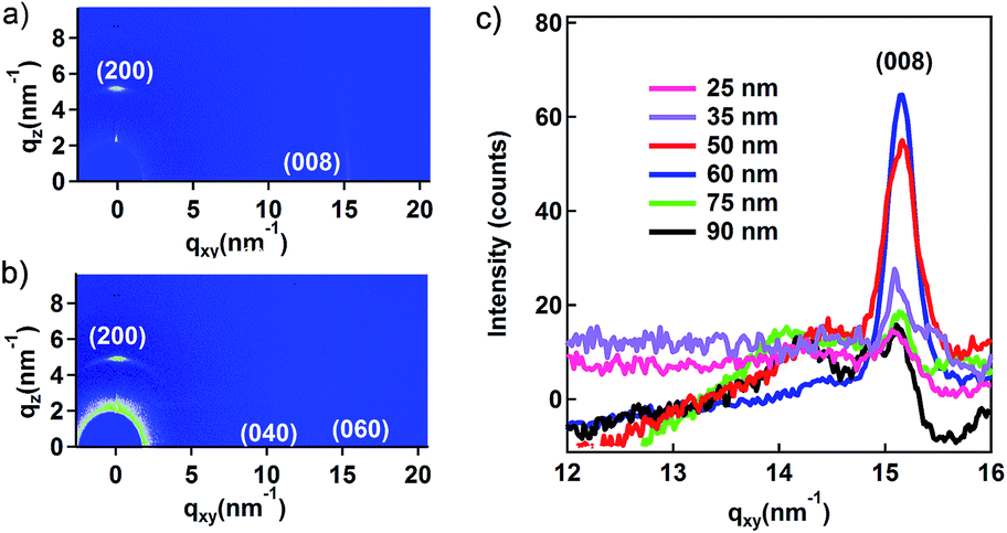 | ||
| Fig. 2 Grazing incidence wide-angle X-rays diffraction (GIWAXD) of the PFO nanogratings. (a) The two-dimensional image of the PFO nanogratings with the initial film thickness about 60 nm and incident X-ray perpendicular to the nanograting. (b) The two-dimensional image with incident X-ray parallel to the nanograting. (c) The one-dimensional integration of the two-dimensional image along qxy with initial film thickness in the range from 25 nm to 90 nm. | ||
The α-conformation PFO can be considered as a rod-like chain, which prefers to align parallel to the grooves as the graphoepitaxial alignment for geometrical and entropic reasons; thus, herein, the chain alignment in the nanograting vector is taken into account. By carefully tuning the initial film thickness of PFO, the protrusion and the residual layer thickness can be precisely controlled, such that the residual layer thickness hr and the protrusion layer thickness hp can be changed. Fig. 2(c) demonstrates that the reflection intensity of X-ray on the plane (008) is changed upon changing both the protrusion and residual layer thicknesses. Based on the GIWAXD result, the crystallinity degree inside these PFO nanogratings can be tuned using different initial film thicknesses. Moreover, we can find out that the best alignment of the molecular chains occur where PFO fully fills in the nano-trench of the PDMS stamp with the lowest residual layer thickness.
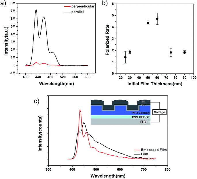
To quantitatively describe the effect of the orientation degree on the initial film thickness of these embossed PFO nanogratings, the polarized UV absorption spectrum was obtained, as shown in Fig. 3. During the polarized absorption spectrum measurement, the polarizer was positioned between the sample and the incident light source. Therefore, when the sample was rotated in plane, the relative angle between the polarizer and the grating vector could be tuned manually. The starting point was set when the polarized direction was parallel to the grating vector, and the absorption spectrum is shown as a black curve in Fig. 3(a). When the relative angle was tuned to 90°, the absorption spectrum was obtained as a red curve, as shown in Fig. 3(a). The PFO nanogratings exhibit the maximum absorption at 390 nm. In addition, the absorbance with the polarization parallel to the nanogratings (I∥) is much stronger than that obtained under perpendicular polarization (I⊥). Since the dipole vector for light absorption of conjugated polymers is typically parallel to the backbones, the anisotropic UV-vis absorption of PFO nanogratings confirms that the polymer backbones are aligned essentially parallel to the nanogratings.28 These results are in good agreement with the structural information obtained from the GIWAXD images. The orientation degree of the embossed PFO grating with different initial film thicknesses could be calculated with the function29

 | ||
| Fig. 3 Absorption analysis of the PFO nanograting. (a) The polarized absorption spectra in the inset figure with the polarized filter direction along (black line) and perpendicular to (red line) the grating vector. (b) The orientation degree with different initial film thicknesses. | ||
As shown in Fig. sp1,† the depth of the nanotrench was around 100 nm. According to the volume conversation law, the thickness of the initial layer should be equal to half of the protrusion and residual thickness. Hence, since the initial layer thickness is lower than 50 nm, the nano-trenches cannot be fully filled by PFO, as shown in Fig. sp3,† and the initial layer thickness higher than 50 nm can result in fully filled nanotrenches and tuneable residual layer thickness. The protrusion thickness was fixed once the initial layer thickness became higher than 50 nm, as shown in the AFM images in Fig. sp3(b) and (c).† As mentioned in ref. 12, confinement scaling can result in different molecular chain alignments; thus, herein, we have discussed the molecular chain alignment mechanism inside the nanogratings after the soft-NIL process. As shown in Fig. sp2,† the imprinting depth and the residual layer thickness could be carefully tuned by different filling states. Before PFO at the initial quantity could fully fill the PDMS stamp, the residual layer thickness was kept constant at around 10 nm. Moreover, the protrusion depth inside the PDMS nano-trenches could be tuned by the initial film thickness. As the protrusion depth increased, the molecular chain arrangement on the top surface was affected by undersurface of the PDMS stamp due to the graphoepitaxial alignment. For geometrical and entropic reasons, the molecular chain orientation was chosen to follow the attachment surface. At the initial film thickness of around 25 or 30 nm, only the side surfaces could provide attachment surfaces for the graphoepitaxial alignment. As the initial film thickness increased, the filling quantity increased as well. Hence, the undersurface in PDMS nanotrenches also became the attachment surface. The top surfaces of the PFO nanogratings were not free any more. All the three surfaces inside the nanotrenches were attachment surfaces for the graphoepitaxial alignment. The nanotrenches in PDMS could be considered as a one-dimensional channel with infinite length. Therefore, the molecular chains prefer to be arranged along the nanotrenches to reduce the volume entropy. When PFO fully filled the nanotrenches, the molecular chain alignment inside the protrusion part reached the upper limit. As the initial film thickness continued to increase, the molecular chain alignment in the protrusion part could not improve further. However, the residual layer was thickened. In the residual layer, the molecular chains were freely arranged without any preferred orientation in the substrate plane as a matter of the entropy principle. Thus, as the residual layer thickened, the overall average of order degree of the (008) planes in the entire PFO nanograting was declined, as shown in Fig. 2.
Besides the X-ray diffraction analysis, polarized absorption was measured to verify this deduction. The PFO nanograting with the initial film thickness of around 60 nm embodied the best performance in the orientation degree. As the 60 nm initial film thickness sample underwent the fully filled state during the nanoimprint process, the (008) planes uniformity reached the upper limit. On the other hand, the residual layer was too thin to affect the entire arrangement of the (008) planes. Hence, the PFO nanograting with the initial film thickness of around 60 nm possessed the best performance in the (008) plane uniformity and the orientation degree. As previously reported, the transition dipoles were off-axis in the molecular chain direction and made an angle of about 26°.30 Therefore, the absolute values of the orientation degree and the polarized rate were not very high. We were convinced that the involvement of the template undersurface could improve the molecular chain alignment further in the soft-NIL process. By the precise control of the filling content, the maximum thick protrusion layer and the minimum thick residual layer could be realized and result in the best molecular chain alignment; this could be greatly helpful in improving the optoelectronic devices.
Since the filling degree in nanotrenches of the PDMS templates had a strong influence on the crystallinity degree and orientation degree, the luminescence property should be optimized by optical pumping. Hence, the polarizability could be tuned; thus, the polarized photoluminescence spectrum was obtained, as shown in Fig. 4(a and b). Polarized photoluminescence spectra were also used to investigate the optical pumping properties of the embossed PFO nanogratings. The polarized photoluminescence spectrum is shown in Fig. 4(b) with the analyzer set between the sample and the emitting detector. The parallel component (the black curve) and the perpendicular component (the red curve) of the photoluminescence spectrum with the initial film thickness of about 60 nm are shown in Fig. 4(a). The polarized rate was an important factor to study the polarized-emitting behaviours and calculated using the function29

 | ||
| Fig. 4 The emission characterization by optical and electrical pumping. (a) The polarization analysis of the emitting light from PFO gratings with the analyzer filter direction along (black line) and perpendicular to (red line) the grating vector. (b) The polarized rate with different initial film thicknesses. (c) The light-emitting intensities at the applied voltage of 5 V on the PFO films with the initial thickness of about 60 nm. | ||
Compared to the surface assistant molecular alignment, this nanoconfinement system in nanoimprint lithography can simultaneously induce the surface structure and the molecular chain alignment. The traditional 5-layer structured PLED was used to study the electronic light-emitting properties of PFO gratings with inner molecular alignment. In this part, about 20 nm PSS:PEDOT film was spin-coated on the patterned ITO electrode; then, α-conformation PFO nanogratings were fabricated on this 20 nm PSS:PEDOT film by nanoimprinting. After this, about 1 nm LiF and 100 nm Al were evaporated on the α-conformation PFO nanogratings. The schematic of the PLED is shown in Fig. 4(c). The electroluminescence (EL) spectrum shown in Fig. 4(c) at the applied voltage of about 5 V indicates that the PFO nanogratings can extract light 20% more than the flat unprocessed films. Herein, samples with the film thickness of about 60 nm are chosen. The embossed PFO nanograting and unembossed PFO film were studied. Although the amount of the luminescent polymer PFO is equal in both cases, the EL intensity of PFO nanogratings with embossed surface is much higher. Many efforts have been focused on luminescence enhancement by inducing patterns of the devices.31–35 Among them, luminescence enhancement can be induced in two ways: (i) modulating the period of the pattern: if the period is about half of the emitting wavelength, the luminescence is enhanced by the output coupling and scattering effect;31 (ii) inducing metal, such as Ag, nanostructures into the pattern; these nanostructures enhance the luminescence by the weak surface plasmon and scattering effects.32 However, in our studies, the period of the PFO gratings is about 600 nm, which is much higher than the half period of the emitting wavelength (450 nm); this results in almost no output coupling and scattering effect. In addition, the height of the PFO nanogratings is lower than 90 nm, whereas the thickness of the Al electrode in our experiments is about 100 nm; hence, the surface plasmonic effect becomes very weak. To study the reason for luminescence enhancement of PFO nanogratings, we measured the photoluminescence quantum efficiency (PQE) of the PFO nanogratings and unprocessed thin films. The PQE is about 36% for the PFO nanogratings, which is about 25% higher than that of the unprocessed thin films (the PQE is about 28%); the PQE improvement can be attributed to the molecular and crystalline alignment, and this improvement results in the PFO nanogratings being able to extract 20% more light than the flat unprocessed films.
Experimental
Preparation of the α-conformation PFO film
The PFO (poly(9,9-dioctylfluorene)) (ADS129BE) was purchased from American dye source company and used as received. The PFO powder was dissolved in toluene and heated to 60 °C overnight for sufficient dissolution. The solution was filtered using 0.25 μm polytetrafluoroethylene filters. The PFO thin films were prepared by spin-coating. The substrates used were quartz glass and the silicon wafer, cleaned using a freshly prepared piranha solution (H2O2 (27%) and H2SO4 (98%) 1:3). The film thickness depended on both the spin speed and the solution concentration. To control the film thickness in the range between 25 nm and 90 nm, the solution concentration was chosen in the range between 10 mg ml−1 and 20 mg ml−1, and the spin speeds were between 2000 rpm and 4000 rpm. The α-conformation thin film achieved by thermal annealing at 180 °C for 5 minutes was slowly cooled down to 135 °C and then slowly cooled down to the room temperature.
Fabrication of the PFO nanogratings
The thin films were transferred to a nano-imprinter (Obducat, Eitre 3) and covered with PDMS (polydimethylsiloxane) template replicated from the polymethylmethacrylate (PMMA) template by E-beam lithography. The height of the PDMS template is about 100 nm. The PDMS templates were pressed against the films under pressure (60 bar) at 180 °C, held at this temperature for 5 min to ensure that nano-trenches in the template were completely filled, then cooled down to 135 °C, held at this temperature for 10 min, and then slowly cooled down to room temperature (30 °C). Before releasing the pressure, the stacks were evacuated to solidify the PFO nanogratings.Fabrication of polymer light-emitting diodes (PLEDs)
The traditional 5-layer structure PLED was used in this study to check the performance improvement by tuning the molecular chain alignment inside. In this part, about 20 nm PSS:PEDOT film was spin-coated on the patterned ITO electrode. Then, α-conformation PFO nanograting was fabricated on this 20 nm PSS:PEDOT film by a nano-imprinter. Moreover, about 1 nm LiF and 100 nm Al were evaporated from the α-conformation PFO nanogratings by high vacuum thermal evaporation with a shadow mask, the area of which was about 9 mm2, which was smaller than that of the PFO nanogratings (64 mm2).Characterization
The thickness of the homogeneous films was measured by a film thickness measurement instrument (F20, Filmetrics, USA) with 1.49 as the refractive index. The morphologies of the PFO films were characterized in the tapping mode of the atomic force microscope (AFM, MFP-3D-SA, Asylum Research, USA) using Pt-coated Si cantilevers (0.2 N m−1 force constant from Nanosensors) and a scanning electronic microscope (SEM, Pioneer, Raith, Germany) at 10 kV. Grazing incidence wide-angle X-rays diffraction (GIWAXD) measurements were carried out at the BL14B1 beam line at the Shanghai synchrotron radiation facility (SSRF) in China. The wavelength and the incident angle of the X-ray beam are 0.12398 nm and 0.18°, respectively. The distance between the sample centre and the two-dimensional charge-coupled device (CCD) detector is 315 mm. Data conversion to q space was accomplished by calibration using LaB6 powder. Polarized UV absorption spectra (UV3600, Shimadzu, Japan) was used to study the orientation degree of PFO nanogratings with different film thicknesses in the transmission mode using a Glan-Thomson polarizer positioned between the sample and the incident light source. The polarized PL spectra (spectrofluorometer, Fluoromax-4, Horiba, USA) were used to study the polarized emission behaviours of the patterned α-conformation PFO film with 380 nm excitation wavelength, and the analyzer was positioned ahead of the emitting detector. The current–voltage and the luminance spectrum characteristics were measured using a constant current source (SourceMeter, Keithley 2400, USA) combined with a photometer (SpectraScan, PR 655, Photo Research, USA). The PQE of the PFO gratings and films were measured using an FLS980 spectrometer (Edinburgh Instruments).Conclusions
A one-step method has been developed to fabricate a PFO thin layer, which can achieve three functions at the same time: patterning, molecular chain alignment, and fluorescence enhancement. Based on the lithography process, patterning and molecular chain alignment can be achieved. Additionally, the crystallinity and the orientation degree can be tuned only by adjusting the PFO layer thickness before the nanoimprinting process, called the initial film thickness. When the initial film thickness reaches the critical value, it makes nanoconfinement the most and the residual layer the least, and this PFO nanograting can reflect highest crystallinity and orientation, as shown in Fig. 2 and 3. We have built the 5-layer PLED devices, and the EL intensity of the PFO nanogratings is 20% higher than that of the flat unprocessed films. We anticipate that the method described herein can also be applied to a wider preparation of materials for the production of high-performance PLEDs due to the ease of use and a substantial increase in device performance.Conflicts of interest
There are no conflicts to declare.Acknowledgements
This work was financially supported by the National Nature Science Foundation of China (No. 21204058, 21074084, 21374069, 21104051 and 91027040) and the BL14B1 Beamline at the Shanghai Synchrotron Radiation Facility in China.Notes and references
- P. D. Cunningham, J. B. Souza Jr, I. Fedin, C. X. She, B. Lee and D. V. Talapin, ACS Nano, 2016, 10(6), 5769 CrossRef CAS PubMed.
- S. I. Jo, Y. Kim, J. H. Baek, C. J. Yu and J. H. Kim, Jpn. J. Appl. Phys., 2014, 53, 03CD04 CrossRef.
- A. Dauendorffer, S. Miyajima, S. Nagamatsu, W. Takashima, S. Hayase and K. Kaneto, Appl. Phys. Express, 2012, 5, 09210 Search PubMed.
- M. F. Toney, T. P. Russell, J. A. Logan, H. Kikuchi, J. M. Sands and S. K. Kumar, Nature, 1995, 374, 709 CrossRef CAS.
- D. Kawakami, B. S. Hsiao, C. Burger, S. F. Ran, C. Avila-Orta, I. Sics, T. Kikutani, K. I. Jacob and B. Chu, Macromolecules, 2005, 38, 91 CrossRef CAS.
- K. Jradi, S. Bistac, M. Schmitt and G. Reiter, Polymer, 2009, 50, 3724 CrossRef CAS.
- N. Tanigaki, C. Heck and T. Mizokuro, Mol. Cryst. Liq. Cryst., 2009, 505, 318 CAS.
- T. Mizokuro, Y. Okamoto, C. Heck, H. Aota and N. Tanigaki, J. Appl. Polym. Sci., 2014, 131, 631 CrossRef.
- S. D. Siqing, H. Wu and A. Takahara, Polymer, 2015, 72, 113 CrossRef CAS.
- T. Matsui, K. Nakayama, M. Ozaki and K. Yoshino, Appl. Phys. Lett., 2000, 76, 1228 CrossRef CAS.
- W. Hu, A. K. Srivastava, X. W. Lin, X. Liang, Z. J. Wu, J. T. Sun, G. Zhu, V. Chigrinov and Y. Q. Lu, Appl. Phys. Lett., 2012, 100, 111116 Search PubMed.
- Z. J. Hu and A. M. Jonas, Soft Matter, 2010, 6, 21 RSC.
- Z. J. Hu, B. Muls, L. Gence, D. A. Serban, J. Hofkens, S. Melinte, B. Nysten, S. Demoustier-Champagne and A. M. Jonas, Nano Lett., 2007, 7, 3639 CrossRef CAS PubMed.
- Z. J. Hu, M. W. Tian, B. Nysten and A. M. Jonas, Nat. Mater., 2009, 8, 62 CrossRef CAS PubMed.
- Q. Zhang, L. Chi, G. Hai, Y. T. Fang, X. C. Li, R. D. Xia, W. Huang and E. Gu, Molecules, 2017, 22, 315 CrossRef PubMed.
- D. Abbaszadeh, N. Y. Doumon, G. A. H. Wetzelaer, L. J. A. Koster and P. W. M. Blom, Synth. Met., 2016, 215, 64 CrossRef CAS.
- A. P. Kulkarni and S. A. Jenekhe, Macromolecules, 2003, 36, 5285 CrossRef CAS.
- K. Sakamoto, K. Miki, M. Misaki, K. Sakaguchi, M. Chikamatsu and R. Azumi, Appl. Phys. Lett., 2007, 91, 183509 CrossRef.
- K. Sakamoto, K. Miki, M. Misaki, K. Sakaguchi, Y. Hijikata, M. Chikamatsu and R. Azumi, J. Appl. Phys., 2010, 107, 113108 CrossRef.
- L. Ghirardini, T. Virgili, S. Bolis, J. Beeckman, P. Kockaert, M. Finazzi and M. Celebrano, J. Polym. Sci., Part B: Polym. Phys., 2016, 54, 1558 CrossRef CAS.
- J. Martin, A. D. Scaccabarozzi, A. Nogales, R. P. Li, D. M. Smilgies and N. Stingelin, Eur. Polym. J., 2016, 81, 650 CrossRef CAS.
- X. H. Li, J. C. Yu, N. Y. Lu, W. D. Zhang, Y. Y. Weng and Z. Gu, Chin. Phys. B, 2015, 24, 104215 CrossRef.
- R. K. Sharma and M. Katiyar, Org. Electron., 2016, 38, 121 CrossRef CAS.
- M. Kitamura, S. Iwamoto and Y. Arakawa, Jpn. J. Appl. Phys., 2005, 44, 2844 CrossRef CAS.
- Y. S. Shim, K. N. Kim, J. H. Hwang, C. H. Park, S. G. J. Y. W. Park and B. K. Ju, Nanotechnology, 2016, 28, 045301 CrossRef PubMed.
- S. H. Chen, H. L. Chou, A. C. Su and S. A. Chen, Macromolecules, 2004, 37, 6833 CrossRef CAS.
- S. H. Chen, A. C. Su, C. H. Su and S. A. Chen, Macromolecules, 2005, 38, 379 CrossRef CAS.
- M. C. Gurau, D. M. DeLongchamp, B. M. Vogel, E. K. Lin, D. A. Fischer, S. Sambasivan and L. J. Richter, Langmuir, 2007, 23, 834 CrossRef CAS PubMed.
- Z. J. Zheng, K. H. Yim, M. S. M. Saifullah, M. E. Welland, R. H. Friend, J. S. Kim and W. T. S. Huck, Nano Lett., 2007, 7, 987 CrossRef CAS PubMed.
- H. M. Liem, P. Etchegoin, K. S. Whitehead and D. D. C. Bradley, Adv. Funct. Mater., 2003, 13, 66 CrossRef CAS.
- L. Zhou, X. C. Jiang, Y. Q. Li, A. L. Shi, J. D. Chen, Q. D. Ou, H. T. Liu and J. X. Tang, ACS Appl. Mater. Interfaces, 2014, 6, 18139 CAS.
- Y. F. Liu, M. H. An, X. L. Zhang, Y. G. Bi, D. Yin, Y. F. Zhang, J. Feng and H. B. Sun, Appl. Phys. Lett., 2016, 109, 193301 CrossRef.
- C. Lee, K. H. Han, K. H. Kim and J. J. Kim, Opt. Express, 2016, 21, A489 Search PubMed.
- K. J. Byeon, H. Park, J. Y. Cho, S. H. Lee, S. Y. Lee, J. O. Song and H. Lee, Current Applied Physics, 2011, 11, S147 CrossRef.
- T. B. Lim, K. H. Kim, S. A. Song, S. N. Lim, K. Y. Kim and Y. C. Jeong, Macromol. Res., 2017, 25, 786 CrossRef CAS.
Footnote |
| † Electronic supplementary information (ESI) available. See DOI: 10.1039/c7ra11602k |
| This journal is © The Royal Society of Chemistry 2017 |