DOI:
10.1039/C7RA11398F
(Paper)
RSC Adv., 2017,
7, 53010-53017
Significant performance improvement of a terahertz photoconductive antenna using a hybrid structure†
Received
16th October 2017
, Accepted 7th November 2017
First published on 16th November 2017
Abstract
A photoconductive terahertz antenna based on a distributed Bragg reflector, recessed nanoplasmonic grating and recessed electrodes is proposed in this paper. By use of the finite element method and full wave simulation, the effect of geometrical parameters on the transient photocurrent of a proposed photoconductive antenna is investigated. The recessed nanoplasmonic structure reduces the reflection of laser light to less than 1.5% from the surface of low temperature gallium arsenide in comparison with 29% for a conventional photoconductive antenna. According to the results, the distributed Bragg reflector in combination with recessed nanoplasmonic grating and recessed electrodes results in 5265% photocurrent peak enhancement in comparison to a conventional photoconductive terahertz antenna.
1. Introduction
The terahertz photoconductive antenna (PCA) has attracted much attention due to the room temperature operation, compact design, broadband radiation and tolerable price.1,2 In this method of terahertz (THz) wave generation, the interaction of an ultrafast laser (e.g. femtosecond (fs) laser) with a biased photoconductive semiconductor results in a transient photocurrent. According to Maxwell electromagnetics, this transient photocurrent with picosecond (ps) pulse width, eventuates to a radiation of electromagnetic waves in the THz spectrum.3 Early investigation by Auston et al. indicates the use of silicon on sapphire (SOS) substrates as an ultrafast photoconductive material for generating THz radiation.4 However, low optical to THz conversion efficiency was obtained because of the indirect band gap of silicon. Later, the substrate was replaced with annealed low temperature grown gallium arsenide (LT-GaAs).5,6 LT-GaAs is one of the most favorable THz semiconductors as it demonstrates ultrafast electron trapping times (ttrap< 1 ps) and has a direct optical band gap of 1.42 eV which is suitable for use with common Ti:Sapphire fs lasers. Moreover, LT-GaAs has high dark resistivity, high carrier mobility, and high thermal and electrical breakdown which are the key parameters for increasing the THz output power and bandwidth of photoconductive materials.7,8 During the last decades, other fast photoconductive semiconductors like InGaAs, AlGaAs, SI-GaAs, SiC, diamond and graphene were introduced as an alternative to LT-GaAs,6,9,10 but the drawbacks such as high carrier lifetimes, low dark resistivity and carrier mobility, energy bandgap, price and fabrication process have not yet let them to be a good substitute for photosensitive material in PCA fabrication industry.11,12
Unique properties of PCA have made it a valuable candidate for THz applications such as in security screening, medical imaging, biomolecules spectroscopy, and others. Despite all advantages, low optical to THz conversion efficiency is the main drawback of PCAs, that limits its application in new areas of science. In practice, PCAs have typical optical to THz conversion efficiency of near 0.01% to 0.1% for the input laser power of 1–50 mW.8,13 Also, the highest conversion efficiency that is based on nanoplasmonic structures was reported to be around 7.5%.14 In the recent years, lots of efforts have been made to optimize the PCA efficiency and improve the output THz power. By increasing the coupling of laser pulse excitation with photosensitive material and confining the laser beam, higher photocarrier density can be obtained and transient photocurrent will increase. In particular, it is shown that antireflection coatings, such as Si3N4 layer on top of PCA photosensitive material can decrease the reflection of laser pulse from 33% to less than 4% and so THz radiation will increase by factor of 5.15 In the other work, AlAs:AlGaAs or AlAs:GaAs layer have been used as a Bragg reflector under the PCA active layer.16 The designed Bragg reflector is transparent for terahertz radiation and it acts as a reflector for 800 nm laser pulse. In a separate study, two kinds of optical nanoantenna have been used in the photosensitive gap of PCA.17 The nanoantenna strongly coupled the illuminated laser beam to the PCA gap and increased the local field near the surface.18,19 By optimizing the geometrical parameters such as periodicity and the height of nanoantennas, the coupling was maximized and the THz wave radiation was shown to improve by factor of two.20
Recently, nanoplasmonic structures have been incorporated on the PCA to improve the efficiency.21–25 In a research, Berry et al. have incorporated a plasmonic grating to the 3 × 3 array of logarithmic spiral antennas fabricated on a LT-GaAs layer.26 They showed that nanoplasmonic resonance at the PCA gap results in high absorption of laser pulse in the photosensitive layer. They have achieved high THz radiation power of 2 mW in the frequency range of 0.1 to 2 THz. In other work, Heshmat et al. illustrated sub-picosecond photocarrier sweep-out and over an order of magnitude higher sensitivity from GaAs based PCA detector by use of nanoplasmonic structure. They observed 40 times peak-to-peak response from the nanoplasmonic structure in comparison with simple surface GaAs.27
In this work, a hybrid structure based on recessed plasmonic nanogratings, recessed electrodes and a distributed Bragg reflector is proposed to maximize the performance of PCAs. The plasmonic nanograting results in high quantum efficiency by reducing the reflection from the surface of LT-GaAs and increasing the light absorption due to the surface plasmon polariton (SPP) excitation. Distributed Bragg reflector (DBR) reflects back the 800 nm fs laser pulse into the LT-GaAs layer and enhances the generation rate inside the photosensitive area. Finally, the recessed electrodes enhance the DC electric field along the depth of the LT-GaAs epilayer which leads to the higher photocarrier collection by the electrodes. The proposed hybrid PCA structure is modeled in this study through detail calculations, as describe below.
2. Structure design and simulation method
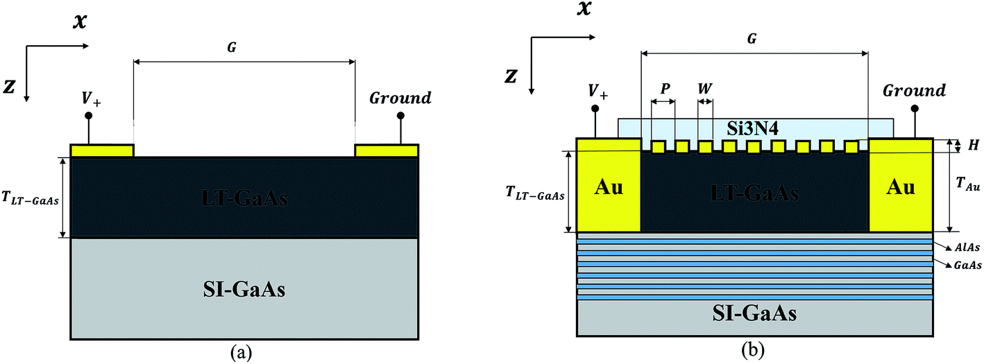
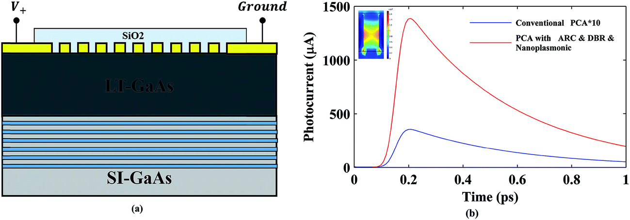
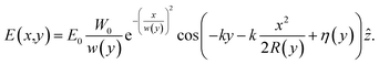
Fig. 1a and b show the schematic diagram of conventional PCA and the proposed hybrid PCA in this study, respectively. The conventional PCA structure consists of 500 nm LT-GaAs on top of infinite semi-insulating (SI) GaAs substrate. Dipole antenna electrodes are 150 nm thick gold which are separated by 5 μm gap. In the proposed structure (Fig. 1b), a recessed gold nanoplasmonic array is located in the PCA gap between the two electrodes. Electrodes are not placed on top of LT-GaAs layer, but are recessed in a way that LT-GaAs layer is sandwiched between them. The distributed Bragg reflector is located between the LT-GaAs layer and the SI-GaAs substrate and it is designed to completely reflect the 800 nm laser pulse back into the photosensitive material and Si3N4 antireflection coating (ARC) has been used to reduce the reflection of laser from LT-GaAs surface. One of the interesting features in our design is the simplicity of fabrication. In order to fabricate this structure, first, it is required to grow the DBR stack layers by use of MBE or MOCVD system on SI-GaAs wafer. Next, the 500 nm LT-GaAs layer has to be deposited on DBR at low temperature (below 250 °C). Afterwards, the recessed nanoplasmonic array has to be patterned using electron beam lithography followed by reactive ion etching of LT-GaAs and deposition of gold nanograting array by evaporation system. As the next step, optical lithography followed by sputtering Ti/Au has to be done to manufacture the PCA electrodes using lift-off technique. At the end, Si3N4 antireflection layer has to be deposited by use of plasma enhanced chemical vapor deposition (PECVD) method. In order to investigate the effect of geometrical parameters such as nanograting periodicity (P), nanograting height (H), nanograting width (W), nanograting depth, DBR layer thickness and electrode depth on PCA photocurrent, the structure was illuminated with 800 nm fs laser pulses.
 |
| | Fig. 1 Schematic diagram of (a) conventional PCA with Si3N4 antireflection coating (ARC) and (b) proposed PCA with DBR, ARC, recessed nanoplasmonic and recessed electrodes. | |
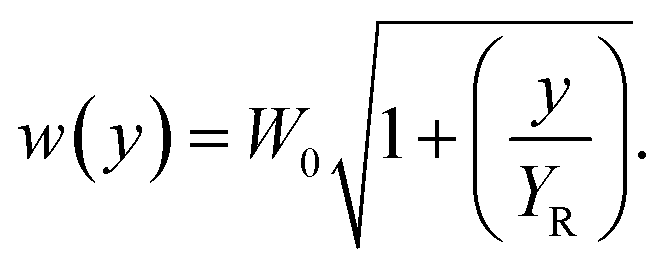
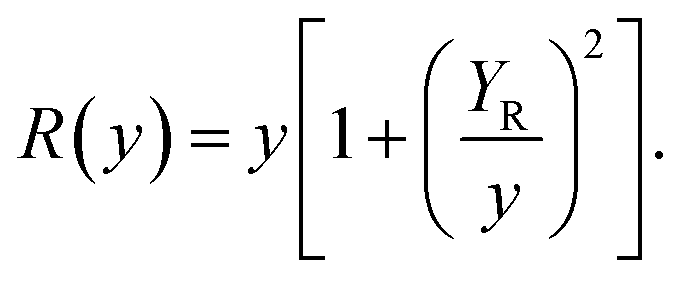
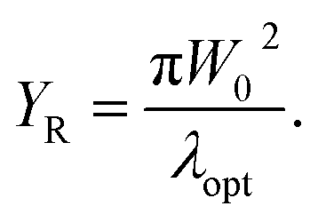
The incident 800 nm fs laser pulse was applied in the form of transverse magnetic (TM) Gaussian electric field, propagating in the Z direction with polarization in the X direction. Thus, the applied electric filed distribution can be described as follow:22
| |
 | (1) |
| |
 | (2) |
| |
 | (3) |
| |
 | (4) |
| |
 | (5) |
| |
 | (6) |
where,
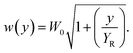
x is the distance from the beam direction,
y is the axial distance from the beam focus (waist),
k is the wave number for the wavelength
λ,
E0 is the electric field amplitude of the origin at time 0,
w(
y) is the radius at which the field amplitude falls to 1/
e of its axial values, at the plane
y along the beam,
W0 is the waist size,
R(
y) is the radius of curvature of the beam's wavefronts at
y, and
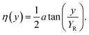
η(
y) is the Gouy phase at
y which is an extra phase term beyond that attributable to the phase velocity of light.
Full wave finite element method (FEM) solver has been used to investigate the proposed structure's electrical and optical behavior by combining the Maxwell's wave equation with the drift-diffusion/Poisson equations. In simulation procedure, first, by solving Maxwell's equation, the optical response was calculated by:21
| |
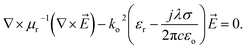 | (7) |
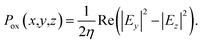
After that, electrical filed distribution in each point of simulation domain has been obtained by solving eqn (7). Power flux density was calculated as followed:
| |
 | (8) |
| |
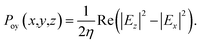 | (9) |
| |
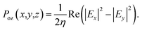 | (10) |
where,
η is material dependent complex wave impedance. The total power flux density can be obtained as followed:
| | |
Ps(x,y,z) = (|Pox(x,y,z)|2 + |Poy(x,y,z)|2 + |Poz(x,y,z)|2).
| (11) |
The time dependent carrier generation rate (G) has been calculated as:28
| |
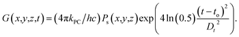 | (12) |
In eqn (12), kPC is the imaginary part of refractive index, c is speed of light, Dt is laser pulse duration and h is Planck's constant. In the next step, transient photocurrent that is the result of laser illumination has been calculated by use of time dependent generation rate combined with transient semiconductor equation (Poisson equation, drift-diffusion and continuity equation). The physical model used here can be described as follow:21
| |
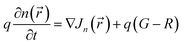 | (13) |
| |
 | (14) |
| |
Jn(![[r with combining right harpoon above (vector)]](https://www.rsc.org/images/entities/i_char_0072_20d1.gif) ) = qμnn(EDC() + E()) + qDn∇n(r) ) = qμnn(EDC() + E()) + qDn∇n(r)
| (15) |
| | |
Jp() = qμpp(EDC() + E()) + qDp∇p(r)
| (16) |
In eqn (13)–(16), n and p are electron and hole density, R is recombination rate, Jn and Jp are current density of electron and hole, respectively, μn and μp are electron and hole mobility, and, Dn and Dp are diffusion coefficient that are related to mobility by Einstein formula.
Calculating the electrical field and the transient generation rate in every point of the structure allows more accurate results in comparison with simple analytical calculations. The maximum value of refined mesh has been set to less than 10 nm to achieve more accurate results. Electrical and optical parameters of simulation are summarized in Table 1.29
Table 1 Material, electrical and optical properties of the structures that used as an input parameter for the simulation
| Parameters |
Values |
| LT-GaAs thickness |
500 nm |
| LT-GaAs permittivity |
12.9 |
| LT-GaAs refractive index, real part |
3.679 |
| LT-GaAs refractive index, imaginary part |
0.063 |
| LT-GaAs band gap |
1.42 eV |
| LT-GaAs affinity |
4.07 eV |
| LT-GaAs carrier lifetime |
Electron: 0.1, hole: 0.4 (ps) |
| LT-GaAs mobility |
Electron: 400, hole: 100 (cm2 V−1 s−1) |
| LT-GaAs electrical conductivity |
1.1 × 10³ S m−1 |
| LT-GaAs intrinsic carrier concentration |
2.1 × 106 cm−3 |
| N-type doping |
1 × 1015 cm−3 |
| Temperature |
300 K |
| DC bias voltage |
15 V |
| Laser pulse free-space wavelength |
800 nm |
| Laser pulse average power |
10 mW |
| Laser pulse repetition rate |
80 MHz |
| Laser pulse width (FWHM) |
50 fs |
| Laser pulse waist (HPBW) |
5 μm |
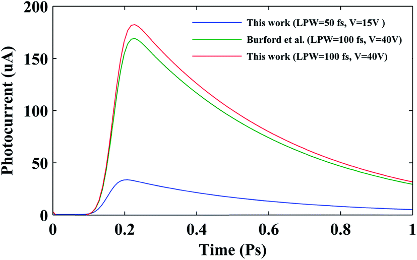
In order to evaluate the validity of our model, the result of simulations for the conventional PCA in this work has been compared to the work of Burford et al.21 Burford et al. have simulated a conventional PCA with 5 μm electrodes' gap by use of FEM method. They have used 10 mW femtosecond laser with pulse width of 100 fs and 40 V as a DC bias. There are notable differences in the two methods. They have obtained the peak photocurrent of 170 μA that is higher than the simulated conventional PCA (35 μA) in this work (Fig. 2). The reason for higher peak photocurrent in their work is because of different laser pulse widths and applied DC voltages. According to Smith et al.,30 the photocurrent of conventional PCA has a linear relation with the applied DC voltage and femtosecond laser pulse width. So, if the applied voltage of our device sets to 40 V and the laser pulse width fixes to 100 fs, the peak photocurrent of conventional PCA in this work will be 186.2 μA that shows less than 10% mismatch to their published data.21
3. Results and discussion
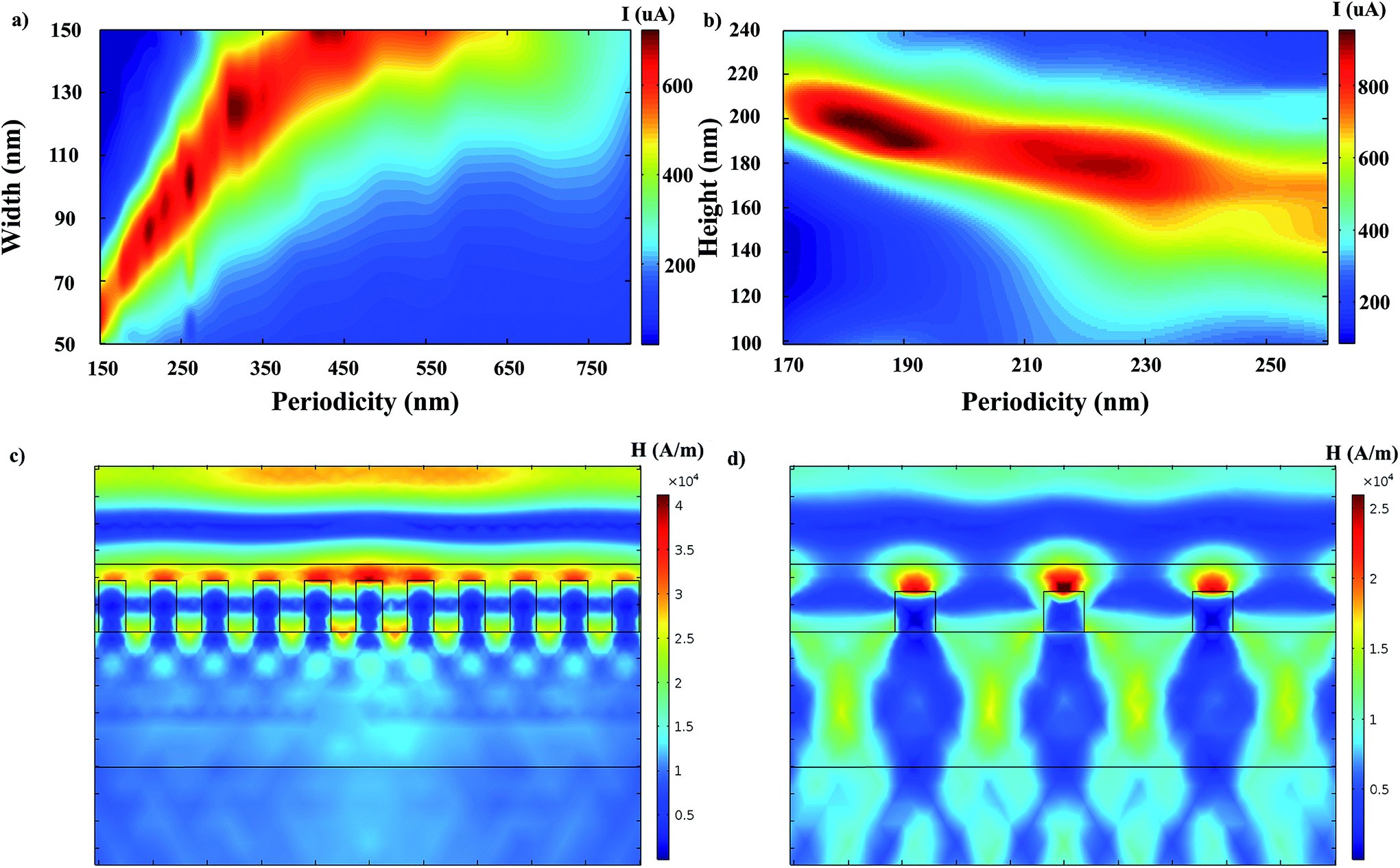
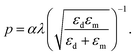
The goal of the proposed design is to maximize the laser beam absorption in the LT-GaAs and to minimize the laser beam transmission out of it. In order to increase photon trapping in the proposed structure, first, an array of gold nanograting with optimized geometrical parameters was placed on top of the LT-GaAs layer. The effects of nanograting periodicity, height and width on the PCA transient photocurrent have been investigated. The calculated photocurrent as a function of nanograting periodicity and width is shown in Fig. 3a. The nanograting height set to H = 150 nm and periodicity (P) swept from 150 nm to 800 nm for the width (w) varying from 50 nm to 150 nm. It is observed that by increasing the width of nanograting, the periodicity of maximum photocurrent moves to higher values. The highest photocurrent of 720 μA is obtained at P = 260 nm and W = 100 nm. When an electromagnetic wave interacts with a nanostructure, energy and momentum conservation between surface plasmon and incident wave has to be satisfied:31,32| |
ksp = kin![[thin space (1/6-em)]](https://www.rsc.org/images/entities/char_2009.gif) sinθ ± mkg. sinθ ± mkg.
| (17) |
| |
 | (19) |
| |
 | (20) |
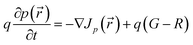
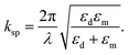
According to the “Effective Medium” method, when an incident wave is perpendicular to the metallic nanostructure array with εm permittivity in a medium with εd permittivity, the effective permittivity relation is:31,33
| |
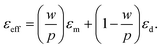 | (21) |
At eqn (17)–(21), ksp is the surface plasmons wave vector, θ is the incident electromagnetic wave angle with surface, kg is the nanostructure wave vector, p is nanostructure periodicity, w is nanostructure width and λ is incident wave wavelength. By assuming the width of nanostructure to 100 nm and using permittivity of different materials and substituting εm in eqn (19) with εeff that has been calculated from eqn (22), the periodicity for the third order mode (α = 3) will be 231 nm, which is in a good agreement with simulation results.
The peak of photocurrent as a function of the periodicity and the height of the nanograting structure is illustrated in Fig. 2b. The highest photocurrent of 940 μA was obtained at P = 190 nm and H = 190 nm. In this step, the width of nanograting was set to 100 nm, which is the highest photocurrent calculated in the last step. According to Fig. 3b, by increasing the periodicity, the optimum height of nanograting varies to smaller values, which indicates fading of plasmonic effect at larger nanostructure heights. As can be seen in Fig. 3c, the plasmonic resonance mode between two adjacent nanostructures is responsible for high photocurrent peak at periodicity of 190 nm that is the same phenomena seen at ref. 34. By increasing the periodicity parameter, as can be observed in Fig. 3d, the surface plasmon polariton appears in the magnetic field distribution on top of the gold nanograting structures which is responsible for trapping the photo-generated carriers at near the surface.
 |
| | Fig. 2 Comparison of the calculated transient photocurrents for conventional PCA in this work with the Burfurd et al.'s (laser pulse width (LPW) = 50 & 100 fs at the applied voltages (V) = 15 & 40 V). | |
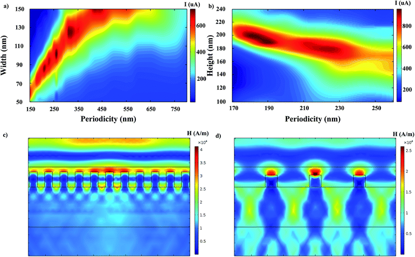 |
| | Fig. 3 (a) Distribution of photocurrent peak as a function of nanograting periodicity (P) and width (W) at nanograting height of H = 150 nm (b) distribution of photocurrent peak as a function of nanograting periodicity (P) and height (H) at nanograting width of W = 100 nm (c) the magnetic field distribution at P = 190 nm, W = 100 nm and H = 190 nm (d) the magnetic field distribution at P = 550 nm, W = 150 nm and H = 150 nm. | |
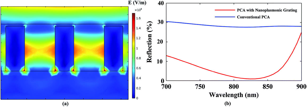
In Fig. 4a and b, the electric field distribution and reflection in the PCA with optimized nanoplasmonic grating (P = 180 nm, W = 100 nm, H = 190 nm) are shown. Local field enhancement around the gold nanostructures is because of plasmon excitation at the interface of metal and dielectric layer. These nanoplasmonic grating structures help to couple the laser pulse beam to the LT-GaAs layer. According to Fig. 4b, the optical reflection of PCA with nanoplasmonic grating and ARC decreases to around 1.5% in comparison with 29% for the conventional PCA without ARC and nanoplasmonic grating at 800 nm wavelength that is less than a value that has been achieved by just Si3N4 ARC.15
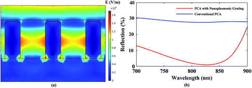 |
| | Fig. 4 (a) Electric field distribution in the PCA with nanoplasmonic grating (P = 180 nm, W = 100 nm, H = 190 nm) (b) comparison of reflection between the conventional PCA and the PCA with optimized nanoplasmonic grating and ARC. | |
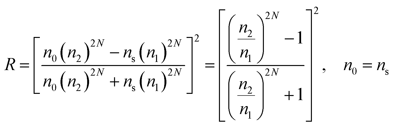
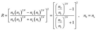
In the next step, a distributed Brag reflector (DBR) structure was examined to increase the laser light path in the LT-GaAs layer by reflecting back the laser pulse into the structure. For this purpose, a periodic structure made of AlAs/GaAs has been used. The sequential layers refractive indexes have to differ as much as possible to maximize the reflectance of the incident light. The reflection coefficient of a DBR can be calculated as follows:35
| |
 | (22) |
In eqn (22), n0 represents active layer refractive index, n1 denotes the first layer of DBR, n2 represents the second layer of DBR, ns denotes the substrate and N represents the number of periods in the DBR. It is obvious that by increasing the number of AlAs/GaAs periods the reflection will be enhanced. By considering the n(AlAs) = 3 and n(GaAs) = 3.6, the reflection coefficient for 10 layers (N = 10) will be R = 0.9. This value increases to 0.983 for N = 15 and for N = 20, this value becomes R = 0.997. Increasing the number of DBR periods results in higher reflection, but on the other hand, complicating the fabrication processes and the cost. So the tradeoff between the maximum reflection and the fabrication complexity is needed. In order to have the best performance, the number of periods (N) was set to 15.
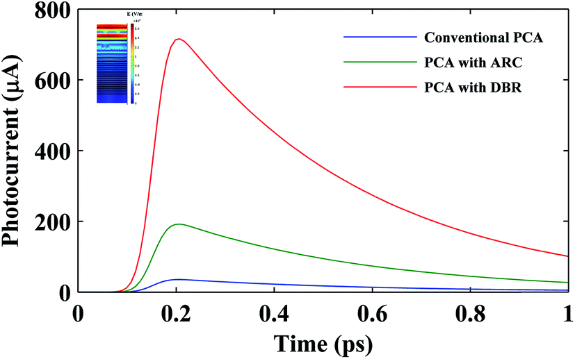
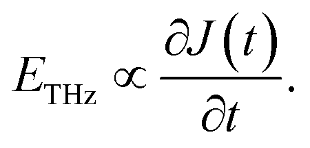
Based on the calculations, Fig. 5 illustrates the comparison of the transient photocurrents between the conventional, antireflection coating-(ARC) and DBR–ARC PCAs. As is shown in this figure, the ARC layer reduces the optical reflection from the surface of LT-GaAs, which results in more optical power inside the LT-GaAs layer and more photocurrent generation in comparison to the conventional PCA. In this figure, the peak of the photocurrent increases more than 445% using SiO2 ARC and more than 1942% using DBR and ARC compared with the conventional PCA. Using DBR between the substrate and the LT-GaAs layer, reflects back much more laser optical power into the LT-GaAs layer and results in increasing the electron–hole generation and the transient photocurrent.
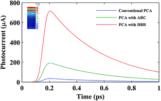 |
| | Fig. 5 Transient photocurrent as a function of time for PCA with DBR and ARC (red line), only ARC (green line), and conventional PCA (blue line). | |
In the next step, the nanoplasmonic grating was combined with the DBR structure to maximize the optical absorption. Fig. 6a and b show the structure design and photocurrent generation of a DBR-enhanced PCA structure with nanoplasmonic grating on top. Using these two structures simultaneously excites the SPP in the LT-GaAs and decreases the optical transmission from the bottom of photosensitive layer. The peak of the photocurrent of 1395 μA were obtained in comparison with 35 μA from conventional PCA, which is more than 3885% enhancement in the transient photocurrent generation. This enhancement will result in a stronger terahertz radiation.
 |
| | Fig. 6 (a) The schematic diagram of the PCA with DBR, ARC and nanoplasmonic grating (b) photocurrent of PCA with DBR, ARC and optimized nanoplasmonic grating. | |
Next in the simulation, deep electrodes were employed to enhance furthermore the PCA's transient photocurrent. For this purpose, the deposited LT-GaAs were etched from the both sides of the device and recessed with Au electrodes. Fig. 7a illustrates the proposed structure of LT-GaAs in between two deep Au electrodes. These electrodes increases the region of static electric field due to the DC dipole biased voltages of PCA. Higher DC field at bottom of LT-GaAs layer results in more photocarrier collection by electrodes, which enhances the transient photocurrent. As is shown in Fig. 7b, the peak of the photocurrent of a PCA with ARC and deep electrode is ∼0.824 mA, that has 2254% improvement in comparison with the conventional PCA and near 15% in comparison with a PCA benefiting from DBR, ARC and elevated electrode.
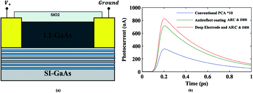 |
| | Fig. 7 (a) The schematic diagram of proposed PCA with DBR and deep electrodes and (b) transient photocurrent of PCA with DBR and deep electrodes (red), DBR and ARC (green), and conventional PCA (blue). | |
In the final step of simulations, recessed nanoplasmonic grating (10 nm) was utilized (Fig. 1b structure). As can be seen in Fig. 8a, deep nanoplasmonic grating results in more plasmon wave penetration into the photosensitive layer and local field enhancement can be observed in a bit greater area inside the LT-GaAs, so more photocarriers will be generated and transient photocurrent will increase. Fig. 8b illustrates the comparison of the photocurrent of different PCAs. The maximum photocurrent of 1.556 mA indicates near 4345% enhancement in comparison to the conventional PCA and near 11.5% enhancement in comparison to the PCA benefiting from DBR, ARC and nanoplasmonic grating.
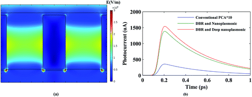 |
| | Fig. 8 (a) The electric field distribution and (b) photocurrent of PCA with DBR, ARC and recessed nanoplasmonic grating. | |
In Table 2, the peak of the photocurrent of different structures have been calculated and compared. Each structure uses a specific scheme to enhance the transient photocurrent. As can be seen in this table, the maximum photocurrent was obtained for the proposed structure, benefitting from DBR, ARC, recessed nanoplasmonic grating and recessed electrodes. By combining these three scheme, the photocurrent peak of 1.877 mA can be obtained with near 5265% photocurrent enhancement in comparison to the conventional PCA. According to the Duvillaret analytical model,36 terahertz radiated electric field is directly proportional to the first order derivative of transient photocurrent of PCA:
| |
 | (23) |
Table 2 Photocurrent peak of different PCA structures mentioned in this study
| |
PCA structure |
Peak photocurrent (μA) |
| 1 |
Conventional |
35 |
| 2 |
SiO2 ARC |
191 |
| 3 |
DBR-SiO2 ARC |
715 |
| 4 |
DBR-SiO2 ARC-recessed electrodes |
824 |
| 5 |
DBR-SiO2 ARC-nanoplasmonic |
1395 |
| 6 |
DBR-SiO2 ARC-recessed nanoplasmonic |
1556 |
| 7 |
DBR-SiO2 ARC-nanoplasmonic-recessed electrodes |
1623 |
| 8 |
DBR-SiO2 ARC-recessed nanoplasmonic-recessed electrodes |
1877 |
So, as can be interpreted from the equation, the enhancement of terahertz field amplitude is almost the same as transient photocurrent enhancement and 5265% enhancement at transient peak photocurrent results in almost 5265% enhancement at terahertz E-field peak. This enormous photocurrent enhancement illustrates the potential of the proposed structure to improve the power conversion efficiency of THz PCAs.
4. Conclusions
In summary, we have illustrated that the distributed Bragg reflector in combination with ARC, recessed nanoplasmonic and recessed electrodes can be used to improve the performance of terahertz PCAs. The effect of nanoplasmonic grating geometrical parameters such as periodicity, height and width on the antenna photocurrent was investigated and the optimized parameters were obtained by using full wave simulations. Nanoplasmonic grating reduces the reflection of 800 nm laser light from 29% for conventional PCA to less than 1.5% for proposed structure and simultaneously excites the plasmon resonance. Additionally, the DBR layer reflects back the laser pulse in to the LT-GaAs and thus increases the optical absorption and so transient photocurrent that finally results in stronger terahertz radiation. The high photocurrent of 1877 μA has been calculated from the proposed structure (DBR, recessed nanoplasmonic grating and recessed electrodes) that indicates ∼5265% enhancement at the photocurrent peak of the antenna in comparison with the conventional PCAs. This large photocurrent enhancement illustrates the potential of the proposed structure for improving the power conversion efficiency of THz PCAs.
Conflicts of interest
There are no conflicts to declare.
Acknowledgements
The authors would like to acknowledge the financial support from IRAN National Science Foundation (INSF) for this project.
References
- M. Tonouchi, Nat. Photonics, 2007, 1, 97–105 CrossRef CAS.
- T. Probst, A. Rehn and M. Koch, Opt. Express, 2015, 23, 21972–21982 CrossRef CAS PubMed.
- J. H. Kim, A. Polley and S. E. Ralph, Opt. Lett., 2005, 30, 2490–2492 CrossRef PubMed.
- D. H. Auston, K. P. Cheung and P. R. Smith, Appl. Phys. Lett., 1984, 45, 284–286 CrossRef.
- F. W. Smith, H. Q. Le, V. Diadiuk, M. a. Hollis, A. R. Calawa, S. Gupta, M. Frankel, D. R. Dykaar, G. a. Mourou and T. Y. Hsiang, Appl. Phys. Lett., 1989, 54, 890–892 CrossRef CAS.
- M. R. Melloch, J. M. Woodall and E. S. Harmon, Annu. Rev. Mater. Sci., 1995, 25, 547–600 CrossRef CAS.
- M. Bashirpour, S. Ghorbani, M. Kolahdouz, M. Neshat, H. Hajhosseini, M. Mansouree and M. Fathipour, in Asia Communications and Photonics Conference 2016, Optical Society of America, 2016, p. AS2E.4 Search PubMed.
- N. M. Burford and M. O. El-Shenawee, Opt. Eng., 2017, 56, 010901 CrossRef.
- A. Singh, S. Pal, H. Surdi, S. S. Prabhu, V. Nanal and R. G. Pillay, Appl. Phys. Lett., 2014, 104, 63501 CrossRef.
- A. Takazato, M. Kamakura, T. Matsui, J. Kitagawa and Y. Kadoya, Appl. Phys. Lett., 2007, 91, 52–54 CrossRef.
- B. Ferguson and X.-C. Zhang, Nat. Mater., 2002, 1, 26–33 CrossRef CAS PubMed.
- F. Akbar, M. Kolahdouz, S. Larimian, B. Radfar and H. H. Radamson, J. Mater. Sci.: Mater. Electron., 2015, 26, 4347–4379 CrossRef CAS.
- N. Khiabani, Y. Huang, Y. C. Shen and S. J. Boyes, IEEE Trans. Antennas Propag., 2013, 61, 1538–1546 CrossRef.
- S. Yang, M. R. Hashemi, C. W. Berry and M. Jarrahi, IEEE Trans. Terahertz Sci. Technol., 2014, 1–7 Search PubMed.
- C. Headley, L. Fu, P. Parkinson, X. Xu, J. Lloyd-Hughes, C. Jagadish and M. B. Johnston, IEEE J. Sel. Top. Quantum Electron., 2011, 17, 17–21 CrossRef CAS.
- O. Mitrofanov, I. Brener, T. S. Luk and J. L. Reno, ACS Photonics, 2015, 2(12), 1763–1768 CrossRef CAS.
- S.-G. Park, Y. Choi, Y.-J. Oh and K.-H. Jeong, Opt. Express, 2012, 20, 25530 CrossRef CAS PubMed.
- S.-H. Yang and M. Jarrahi, Opt. Lett., 2013, 38, 3677–3679 CrossRef CAS PubMed.
- A. Jooshesh, L. Smith, M. Masnadi-Shirazi, V. Bahrami-Yekta, T. Tiedje, T. E. Darcie and R. Gordon, Opt. Express, 2014, 22, 27992 CrossRef PubMed.
- H. Surdi, A. Singh and S. S. Prabhu, Proceeding 2013 COMSOL, 2013, pp. 1–5 Search PubMed.
- N. Burford and M. El-Shenawee, J. Opt. Soc. Am. B, 2016, 33, 748–759 CrossRef CAS.
- S. Ghorbani, M. Bashirpour, M. Kolahdouz, M. Neshat, M. Mansouree and M. Forouzmehr, in Asia Communications and Photonics Conference 2016, Optical Society of America, 2016, p. AF2A.73 Search PubMed.
- S. Jafarlou, M. Neshat and S. Safavi-Naeini, Opt. Express, 2013, 21, 11115–11124 CrossRef PubMed.
- S. Yang and M. Jarrahi, Opt. Express, 2015, 23, 28522–28530 CrossRef CAS PubMed.
- M. Bashirpour, M. Kolahdouz and M. Neshat, Vacuum, 2017, 146, 430–436 CrossRef CAS.
- C. W. Berry, M. R. Hashemi and M. Jarrahi, Appl. Phys. Lett., 2014, 104, 81122 CrossRef.
- B. Heshmat, H. Pahlevaninezhad, Y. Pang, M. Masnadi-Shirazi, R. Burton Lewis, T. Tiedje, R. Gordon and T. E. Darcie, Nano Lett., 2012, 12, 6255–6259 CrossRef CAS PubMed.
- S. L. Chuang, Physics of Photonic Devices, Wiley Online Library, 2009 Search PubMed.
- M. Khabiri, M. Neshat and S. Safavi-Naeini, IEEE Trans. Terahertz Sci. Technol., 2012, 2, 605–616 CrossRef.
- P. R. Smith, D. H. Auston and M. C. Nuss, IEEE J. Quantum Electron., 1988, 24, 255–260 CrossRef.
- S. A. Maier, Plasmonics: fundamentals and applications, Springer Science & Business Media, 2007 Search PubMed.
- R. Wang, T. Li, X. Shao, X. Li and H. Gong, AIP Adv., 2015, 5, 1–6 Search PubMed.
- M. H. Tyboroski, N. R. Anderson and R. E. Camley, J. Appl. Phys., 2014, 115, 13104 CrossRef.
- M. J. Mohammad-Zamani, M. Neshat and M. K. Moravvej-Farshi, Opt. Lett., 2016, 41, 420–423 CrossRef PubMed.
- C. J. R. Sheppard, Pure Appl. Opt., 1995, 4, 665–669 CrossRef.
- L. Duvillaret, F. Garet, J.-F. Roux, J.-L. Coutaz, J.-L. C. L. Duvillaret, F. Garet and J.-F. Roux, IEEE J. Sel. Top. Quantum Electron., 2001, 7, 615–623 CrossRef CAS.
Footnote |
| † Electronic supplementary information (ESI) available. See DOI: 10.1039/c7ra11398f |
|
| This journal is © The Royal Society of Chemistry 2017 |
Click here to see how this site uses Cookies. View our privacy policy here. 
 Open Access Article
 This Open Access Article is licensed under a
  *,
M. Neshat,
M. Masnadi-Shirazi and
H. Aghababa
*,
M. Neshat,
M. Masnadi-Shirazi and
H. Aghababa