DOI:
10.1039/C7RA11186J
(Paper)
RSC Adv., 2017,
7, 49649-49654
A dual-functional surface with hierarchical micro/nanostructure arrays for self-cleaning and antireflection
Received
11th October 2017
, Accepted 18th October 2017
First published on 25th October 2017
Abstract
Surfaces with hierarchical micro/nanostructures have been widely fabricated for their extensive applications in self-cleaning, antireflection, etc. However, a flexible and highly efficient method for obtaining such surfaces remains a great challenge, especially for metals. In this paper, we propose a simple and tunable approach for fabricating a dual-functional surface with patterned hierarchical micro/nanostructure arrays. A femtosecond laser was used to remove the SiO2 thin film, coated on the Cu substrate, masklessly and selectively. Then the arrays of micro-protrusions decorated with nanoneedles were synthesized successfully through thermal oxidation. We demonstrate that the morphology of the micro-protrusions remarkably affects the surface properties, which can be flexibly tuned by controlling femtosecond laser parameters. By optimizing the laser parameters (e.g. scanning mode and laser fluence), we can achieve high performances with respect to superhydrophobicity, with a maximum contact angle of 161° and extremely low adhesion with a minimum sliding angle of less than 1.7°, thus demonstrating its self-cleaning function. In addition, antireflection properties with a minimum reflectance of less than 1% at a wavelength range of 700–800 nm can be achieved and the total reflectance can be steadily below 6% over a broad wavelength range of 600–1150 nm.
Introduction
Over the past decades, micro/nanostructures have received considerable research interest because of their extensive applications in self-cleaning,1–6 oil–water separation,2,7,8 anticorrosion,3,4,9 optical enhancement,5,10–12 water splitting,13 catalyst,14–16 antireflection,17,18 and surface-enhanced Raman spectroscopy detection.3,6,19–21 There are plenty of hierarchical micro/nanostructure surfaces which have been inspired by nature.22–26 Jiang et al. reviewed the designs of bioinspired multifunctional materials27 and indicated that biological surfaces have some unique properties e.g. wettability, mechanical properties, structure color, and optical properties. The wettability of superhydrophobic surfaces with a static contact angle (CA) greater than 150° and a sliding angle less than 10° is mainly determined by the chemical composition, surface roughness, and geometric morphology.28 In particular, surfaces bioinspired by the lotus leaf effect29,30 have been increasingly researched because of their superhydrophobicity. The superhydrophobicity of lotus leaves mainly depends on the hierarchical micro/nanostructures rather than the effect of the plant epicuticular wax that provides a primary waterproof barrier and protection against different environments. To obtain the analogy of superhydrophobicity surfaces with respect to the lotus leaf effect, it is necessary to fabricate hierarchical micro/nanostructures.
Recently, many hierarchical micro/nanostructures have been fabricated using conventional methods such as electrochemical processes,31 lithography,32 and galvanic replacement reaction.33 For example, Yang et al. shown that the morphology of superhydrophobicity surfaces can be changed from cauliflower-like to dendritic-like through a galvanic replacement reaction with different concentrations of AgNO3 solution.33 However, this reaction in solution is less controllable and cannot achieve patterned micro/nano-structures. Zhang et al. reported hetero-hierarchical micro/nanostructures on Cu foils with a CA of 165° and a sliding angle of less than 2° using photolithography coupled with electrochemical deposition.3 Although patterned micro/nanostructures have been achieved using this method to obtain superhydrophobicity surfaces, the photomasks used in photolithography are complicated and expensive,34 limiting their further industrial applications. Femtosecond laser processing is a one-step direct maskless fabrication technique and has intrinsic advantages over traditional methods with respect to controllability and economy.35,36
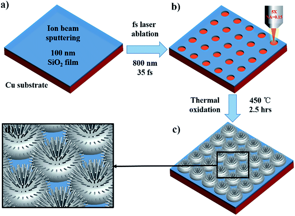
In this paper, we propose a simple and tunable approach for fabricating a dual-functional surface with patterned hierarchical micro/nanostructure arrays. The fabrication process is illustrated in Fig. 1. First, the Cu substrate was coated with a SiO2 film through ion beam sputtering. Subsequently, a uniform dot or line array was fabricated using a femtosecond laser. Finally, an array of micro-protrusions decorated with CuO nanoneedles was generated using thermal oxidation in a muffle furnace. The prepared hierarchical micro/nanostructures were CuO micro-protrusions decorated with CuO nanoneedles, exhibiting excellent superhydrophobicity and antireflection properties over a broad range of wavelengths.
 |
| | Fig. 1 Schematic procedures of the micro/nanostructures fabrication. (a) Prepared Cu substrate with SiO2 film coated by ion beam sputtering. (b) Removal of SiO2 thin film using femtosecond laser. (c) CuO micro/nanostructure growing on substrate after thermal oxidation. (d) Magnified structure units. | |
Experimental
Materials
Polished Cu substrates (10 mm × 10 mm × 1 mm, 99.9999% purity) were purchased from Hefei Kejing Materials Technology Co., Ltd. The Cu substrates were coated with a 100 nm-thick SiO2 film through ion beam sputtering.
Laser ablation of the SiO2 thin film on a Cu substrate
The patterned dot and line arrays were fabricated using a mode-locked Ti: sapphire laser system (Spectra Physics, Inc., Santa Clara, California, USA; 800 nm, 35 fs, 1 kHz). The Gaussian profile laser beam was focused perpendicular to the substrate by an objective lens (Olympus MPLFLN 5×; numerical aperture [NA] = 0.15). The Cu sample was mounted on a six-axis motion stage (M-840.5DG, PI, Inc., Karlsruhe, Germany) with a resolution of 1 μm in the XY directions and 0.5 μm in the Z direction. The motion stage was computer-controlled to efficiently fabricate the dot and line array structure. The laser fluence was adjusted from 0.9 to 10.5 J cm−2 while fabricating the dot array, and the laser fluence was adjusted from 0.54 to 1.2 J cm−2 while fabricating the line array. The dot-to-dot spacing was 15 μm and the line-to-line spacing was 10 μm. After laser ablation, all the samples were cleaned ultrasonically with deionized water and alcohol for 5 min to remove debris.
Thermal oxidation
After the laser ablation, the samples were heated at 450 °C for 2.5 h in a muffle furnace (GHA12/300, Carbolite) to grow CuO micro-protrusions decorated with CuO nanoneedles. Then, the samples were cooled to room temperature.
Characterization
The sample surface was characterized using a scanning electron microscope (SEM, FEI XL30 S-FEG). The composition of the hierarchical micro/nanostructures was analyzed through energy dispersive X-ray spectroscopy (EDX). The surface water contact angles were measured using an optical contact angle measuring system (OCA 15 Pro, Dataphysics Inc.) and SCA 20 measuring software through a sessile drop technique. Reflectance was measured through Fourier-transform infrared spectroscopy (FT-IR, Vertex 70, Bruker) using the polished Cu surface as the background signal and the fabricated surface as the sample signal.
Results and discussion
Microdot arrays fabricated using femtosecond laser
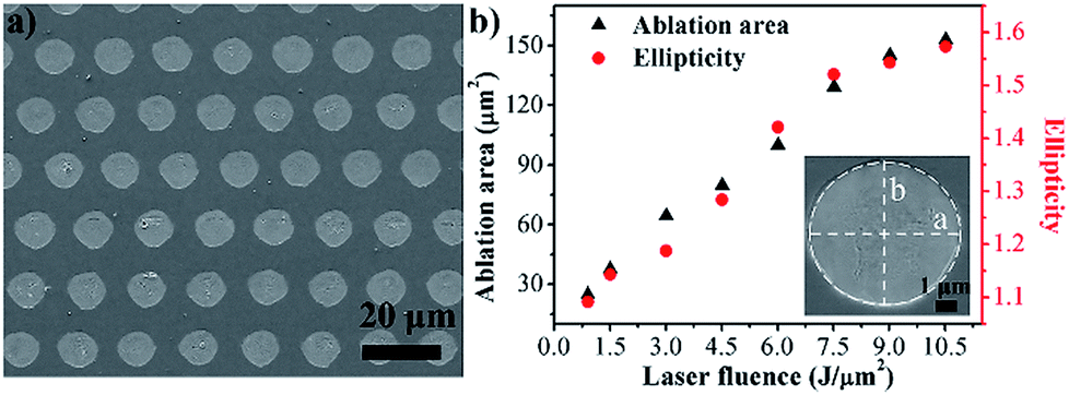
The laser ablation of SiO2 thin films coated on bulk materials has been a topic of considerable researches in recent years.37–41 Most previous studies have focused on SiO2 films on Si substrates, and the mechanism of film ablation has typically been explained by a model of melting and vaporization.37 The ablation of a SiO2 thin film on a Cu substrate could be understood to be a similar process. The results of a microdot array fabricated using a femtosecond laser are shown in Fig. 2. Fig. 2(a) shows an SEM image of the patterned microdot array fabricated through femtosecond laser ablation of the SiO2 film coated on the Cu substrate. The patterned microdot array could be achieved by femtosecond laser selective single-pulse ablation. The magnified SEM image of the ablated craters is shown in the insets of Fig. 2(b). The SiO2 film was completely removed through femtosecond laser ablation while the Cu substrate was almost undamaged, which is similar to a previous report on femtosecond laser ablation of a SiO2 film on a Si substrate.39 Moreover, the microdots exhibited an elliptical geometric morphology, wherein the major axis was parallel to the direction of laser polarization. A similar phenomenon has been reported in previous studies on femtosecond laser ablation of Si and Cu.42,43 To qualitatively depict the aforementioned ellipticity of the ablated microdots, we defined parameter ellipticity as the aspect ratio of a to b, where a and b represent the lengths of the major axis and minor axis, respectively. The dependence of the ablation area and ellipticity on the laser fluence is shown in Fig. 2(b). The ablation area of the SiO2 film increased as the laser fluence increased. That is, the size of the microdots can be controlled by adjusting the laser fluence. However, the laser fluence should not exceed certain threshold in order to prevent the Cu substrate from damage. Similarly, the ellipticity also increased with an increase in the laser fluence, as shown in Fig. 2(b). To explain this polarization-dependence phenomenon, anisotropic energy absorption should be considered. The energy of a polarized femtosecond laser is absorbed more efficiently along the laser polarization direction, as described by Fresnel coefficients.44 This anisotropic energy absorption effect facilitates the preferred ablation along the laser polarization.
 |
| | Fig. 2 (a) SEM image of the dot array fabricated through femtosecond laser ablation of SiO2 film coated on the Cu substrate (laser repetition: 100 Hz; scanning speed: 1500 μm s−1; laser fluence: 1.5 J cm−2). (b) Dependence of ablation area and ellipticity on the laser fluence. The laser fluences were varied from 0.9 to 10.5 J cm−2. The inset is an SEM image of a microdot marked by dash lines, which represent the ablation area, the major axis, and the minor axis, respectively. | |
Thermal oxidation of the dot array
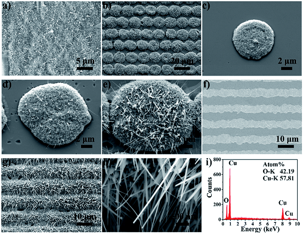
CuO nanoneedles can be easily synthesized by heating a Cu substrate.46 Herein, after femtosecond laser ablation of the SiO2 thin film, the samples were placed in a muffle furnace to induce thermal oxidation. The parameters of thermal oxidation are important to obtain uniform micro-protrusions decorated with nanoneedles. In this study, all the samples were heated at 450 °C for 2.5 h. Fig. 3(a) shows the SEM image of CuO nanoneedles formed on a bare Cu surface after thermal oxidation. The Cu surface was completely covered with CuO nanoneedles after thermal oxidation, but the resulting surface was inhomogeneous in space, which is consistent with a previous report.46 Fig. 3(b) shows the SEM image of a microdot array patterned through femtosecond laser ablation and thermal oxidation. The laser fluence of the femtosecond laser ablation was 6 J cm−2. After selective ablation of the SiO2 film, the Cu substrate was exposed to air. After thermal oxidation, the exposed Cu was oxidized to form CuO micro-protrusions decorated with nanoneedles, as shown in Fig. 3(b). The effects of the femtosecond laser fluences used in the ablation of the SiO2 film are illustrated in Fig. 3(c–e). Few CuO nanoneedles were formed on the micro-protrusion at 1.5 J cm−2 (Fig. 3(c)). However, when the laser fluence was increased to 3.0 J cm−2, some CuO nanoneedles were generated on the edge of the micro-protrusions (Fig. 3(d)). Abundant CuO nanoneedles were fabricated on the micro-protrusion at 6.0 J cm−2 (Fig. 3(e)). Moreover, the size of the micro-protrusions apparently increased with an increase of the laser fluence. Therefore, the femtosecond laser fluence considerably affects the subsequent growth performance of the thermal oxidation process. That is, the size of the micro-protrusions and the morphology of the CuO nanoneedles can be adequately controlled using tunable femtosecond laser fluence.
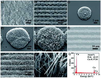 |
| | Fig. 3 (a) SEM image of CuO nanoneedles formed on bare Cu surface after thermal oxidation. The thermal oxidation lasted for 2.5 h at 450 °C. (b) SEM image of microdot array patterned through femtosecond laser ablation and thermal oxidation when the was 6.0 J cm−2. (c–e) SEM images of micro-protrusion decorated with CuO nanoneedles after femtosecond laser ablation and thermal oxidation at different laser fluences: (c) 1.5, (d) 3.0, and (e) 6.0 J cm−2. (f) SEM image of the microline array after femtosecond laser ablation of the SiO2 film (laser repetition: 1000 Hz; scanning speed: 1000 μm s−1; laser fluence: 0.60 J cm−2). (g) SEM image of microridges decorated with CuO nanoneedles after femtosecond laser ablation and thermal oxidation. (h) Detailed view of the nanoneedles. (i) EDX result of the hierarchical line array. | |
Results of the line array
Femtosecond laser direct writing is a maskless technique for fabricating complicated structures with arbitrary shapes through programmed control. Except for the dot array, the line array can also be fabricated through femtosecond laser direct writing. Fig. 3(f) shows the SEM image of the microline array after femtosecond laser ablation of the SiO2 film. The edge of the ablated SiO2 film was slightly irregular because of the vibration of the motion stage. After thermal oxidation, the exposed Cu surface was oxidized to form CuO microridges decorated with abundant CuO nanoneedles (Fig. 3(g)). A further magnified SEM image shows that the diameters of certain nanoneedles were 55 nm and 23 nm (Fig. 3(h)). The EDX result in Fig. 3(i) indicates that the hierarchical line array comprised Cu and O elements. The chemical reactions involved in the formation of CuO can be given as follows:45,47,48
Wetting properties
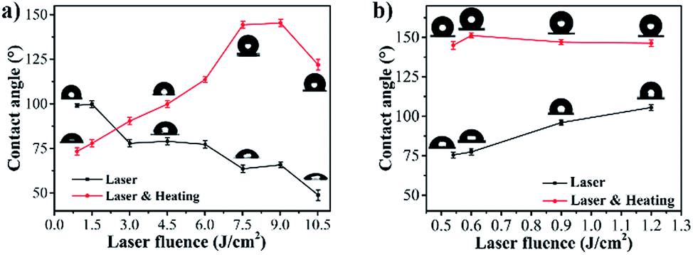
The wettability of the aforementioned prepared samples was further explored by testing the water contact angle (CA) in air. Fig. 4 illustrates the water CAs of hierarchical dot array and line array structures fabricated at different laser fluences before and after thermal oxidation. Before thermal oxidation, the CA of the dot array decreased from 99.2° to 48.9° as the laser fluences increased from 0.9 to 10.5 J cm−2, exhibiting increasing hydrophilicity (Fig. 4(a), black line). However, after thermal oxidation, the CA of the dot array initially increased with the laser fluence and then decreased as the laser fluence exceeded 9.0 J cm−2 (Fig. 4(a), red line). The maximum CA could be 145.4°, indicating the hydrophobic property. Regarding the line array structure, the CA increased from 75.5° to 105.6° as the laser fluence increased from 0.54 to 1.2 J cm−2 before thermal oxidation, exhibiting increasing hydrophobicity (Fig. 4(b), black line). After thermal oxidation, the CA of the line array initially increased with the laser fluence and then decreased as the laser fluence exceeded 0.6 J cm−2 (Fig. 4(b), red line). The maximum CA could be 152° without any chemical modification when the laser fluence was 0.6 J cm−2, indicating superhydrophobicity. It is worth noting that the Cu substrate would show severe damage when the laser fluence is higher than 1.2 J cm−2.
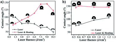 |
| | Fig. 4 Water contact angles of (a) hierarchical dot array and (b) hierarchical line array structures fabricated by different pulse energies before and after thermal oxidation. | |
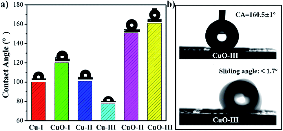
Fig. 5(a) displays a comparison of the water CA for different surfaces. As illustrated in Fig. 5(a), the bare Cu substrate (Cu-I) was slightly hydrophobic with a CA of 100°. When subjected to thermal oxidation, the smooth Cu surface was oxidized into abundant CuO nanoneedles, corresponding to Fig. 3(a). Because of the existence of CuO nanoneedles, the CA of the CuO surface (CuO-I) increased to 120°. When the Cu substrate was coated with a 100 nm-thick SiO2 thin film (Cu-II), the CA was approximately 101° and remained almost unchanged compared with Cu-I. When irradiated by femtosecond laser, the SiO2 film was selectively ablated. The CA of the line array structures (Cu-III) was approximately 77.4°, indicating a decrease in CA after femtosecond laser ablation of the SiO2 film at the fluence of 0.60 J cm−2. However, after the thermal oxidation process, the CA of the line array (CuO-II) substantially increased to 152°, exhibiting the superhydrophobicity of this surface without any chemical modification. In other words, the wetting properties of the surface can be controlled from hydrophilicity to superhydrophobicity by the thermal oxidation process. To further improve the wetting properties, the chemical modification of the thermal-oxidized line array (CuO-II) could be achieved by silanization. After chemical modification, the CA of the surface (CuO-III) was approximately 160.5°. For a superhydrophobic surface, the sliding angle can reflect the adhesive force of water on the surface, which is defined as the critical angle at which the water begins to roll off the inclined plate. As shown in Fig. 5(b), the sliding angle of CuO-III was less than 1.7°, indicating that the water droplet could not adhere well on this superhydrophobic surface. Thus, the CuO-III surface was determined to have the best superhydrophobicity and lowest adhesion among all the fabricated surfaces.
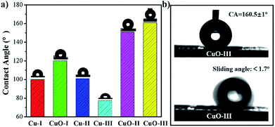 |
| | Fig. 5 (a) Comparison of the water contact angle on different surfaces. Cu-I represent bare Cu surface. CuO-I represents bare Cu surface after thermal oxidation. Cu-II represents bare Cu surface coated with 100 nm SiO2 film. Cu-III represents the line array structures fabricated by fs laser at the fluence of 0.60 J cm−2 before thermal oxidation. CuO-II represents line array structures fabricated by fs laser at the fluence of 0.60 J cm−2 after thermal oxidation. CuO-III represents line array structures fabricated by fs laser at the fluence of 0.60 J cm−2 after thermal oxidation and chemical modification. (b) Contact angle and sliding angle of CuO-III. | |
Self-cleaning
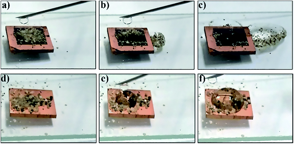
A hierarchical micro/nanostructure line array usually has the property of self-cleaning due to its superhydrophobicity and low adhesion. To demonstrate the self-cleaning behaviour of different surfaces, sand particles were covered on the surfaces as contaminants. The process of a series of water droplets dripped on the CuO-III surface is shown in Fig. 6(a–c). The water droplets rolled off quickly and removed the contaminants on the CuO-III surface, exhibiting the considerable self-cleaning effect of the surface. The process of a series of water droplets dripped on the bare Cu surface is shown in Fig. 6(d–f). The water droplets stuck to the sand particles and stayed on the bare Cu surface, showing no self-cleaning effect. Through the self-cleaning experiments, the CuO-III surface with the hierarchical micro/nanostructure line array can be concluded to have great self-cleaning performance.
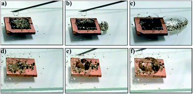 |
| | Fig. 6 Self-cleaning process on different surfaces: (a–c) the line array structures fabricated by fs laser at the fluence of 0.60 J cm−2 after thermal oxidation and chemical modification, (d–f) bare copper surface. | |
Antireflection
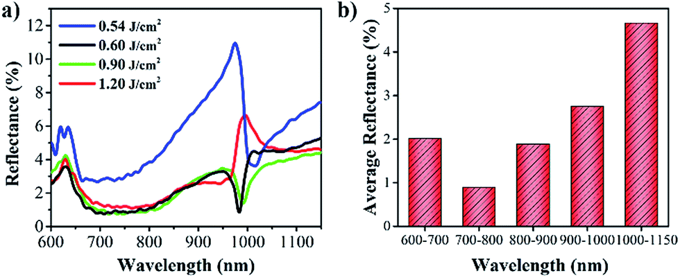
Micro/nanostructures have applications in antireflection, such as nanoneedles and nanocones.10 In this study, the hierarchical micro/nanostructure line arrays fabricated using different laser fluences exhibited high antireflective performance over a broad range of wavelengths (600–1150 nm), as illustrated in Fig. 7(a). The reflection spectra for the hierarchical micro/nanostructure line array surfaces decreased to less than 11% over a broad wavelength range. In particular, the SiO2 thin film was removed at a fluence of 0.54 J cm−2; thus, the microridges and nanoneedles were not sufficiently abundant to trap the light (Fig. 7(a)). As the laser fluence increased, the growth of microridges and nanoneedles significantly increased. The microridges and nanoneedles could impart stronger geometrical light trapping effects to the sample surfaces, thereby resulting in lower reflectance.17 Particularly, the CuO nanoneedles could induce phonon dissipation and eliminate the incident photons' energy through multi-internal reflection among the oxide nanoneedles while achieving a much lower overall surface reflectance.17 Therefore, the total reflectance of the sample considerably decreased to less than 6% in 600–1150 nm range when the laser fluence slightly increased to 0.60 J cm−2. However, when the laser fluence was further increased, the reflectance of the samples hardly remained unchanged. Fig. 7(b) shows the average reflectance in different wavelength ranges for the hierarchical micro/nanostructure line array surfaces fabricated at the laser fluence of 0.60 J cm−2. It shows that the arithmetic average values of the measured reflectance in the 600–700 nm, 700–800 nm, and 800–900 nm ranges were all lower than 2%. In particular, the average reflectance decreased to less than 1% in the 700–800 nm range. Overall, the average reflectance was all lower than 5% in 600–1150 nm range.
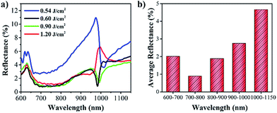 |
| | Fig. 7 (a) Reflectance of hierarchical micro/nanostructure line array surfaces fabricated at different laser fluences and under the same thermal oxidation condition. Polished Cu surface was set as the reference substrate with a reflectance of 100%. (b) Average reflectance in different wavelengths ranges for hierarchical micro/nanostructure line array surfaces fabricated at a laser fluence of 0.60 J cm−2. | |
Conclusions
In this study, hierarchical micro/nanostructure arrays with superhydrophobicity, self-cleaning and antireflection properties were fabricated by femtosecond laser ablation and thermal oxidation method. The morphologies of CuO micro-protrusions and the nanoneedles could be well tuned by controlling the femtosecond laser energy to obtain the desired surface properties. The line array surface could exhibit optimal superhydrophobicity with the contact angle and sliding angle of approximately 161° and 1.7°, respectively, exhibiting excellent self-cleaning effect. Through the light trapping in the micro/nanostructures, the reflectance could be less than 1% at the 700–800 nm wavelength range and keep steadily below 6% over a broad wavelength range of 600–1150 nm. Moreover, both the highly ordered micro-protrusions and the nanoneedles can be effectively reproduced, representing significant advantages for practical application. Besides, our approach may be suitable for processing large-area micro/nanostructures on various metallic materials.
Conflicts of interest
There are no conflicts to declare.
Acknowledgements
This work was supported by the National Natural Science Foundation of China (NSFC) (Grant No. 91323301 and 51675048), and the 863 of Ministry of Science and Technology of China (Grant No. 2015AA042702).
Notes and references
- Z. Guo, X. Chen, J. Li, J. H. Liu and X. J. Huang, Langmuir, 2011, 27, 6193–6200 CrossRef CAS PubMed.
- L. Zhang, Y. Zhong, D. Cha and P. Wang, Sci. Rep., 2013, 3, 2326 CrossRef PubMed.
- Q. X. Zhang, Y. X. Chen, Z. Guo, H. L. Liu, D. P. Wang and X. J. Huang, ACS Appl. Mater. Interfaces, 2013, 5, 10633–10642 CAS.
- F. Su and K. Yao, ACS Appl. Mater. Interfaces, 2014, 6, 8762–8770 CAS.
- A. Y. Vorobyev and C. Guo, J. Appl. Phys., 2015, 117, 033103 Search PubMed.
- X. Du, Y. Xing, X. Li, H. Huang, Z. Geng, J. He, Y. Wen and X. Zhang, RSC Adv., 2016, 6, 7864–7871 RSC.
- X. Gao, J. Zhou, R. Du, Z. Xie, S. Deng, R. Liu, Z. Liu and J. Zhang, Adv. Mater., 2016, 28, 168–173 CrossRef CAS PubMed.
- S. Ye, Q. Cao, Q. Wang, T. Wang and Q. Peng, Sci. Rep., 2016, 6, 37591 CrossRef CAS PubMed.
- W. Zhao, X. Liu, Y. Xu, S. Wang, T. Sun, S. Liu, X. Wu and Z. Xu, RSC Adv., 2016, 6, 35527–35531 RSC.
- J. Zhu, Z. Yu, G. F. Burkhard, C.-M. Hsu, S. T. Connor, Y. Xu, Q. Wang, M. McGehee, S. Fan and Y. Cui, Nano Lett., 2008, 9, 279–282 CrossRef PubMed.
- T. Hussain, L. Zhong, M. Danesh, H. Ye, Z. Liang, D. Xiao, C. W. Qiu, C. Lou, L. Chi and L. Jiang, Nanoscale, 2015, 7, 10350–10356 RSC.
- J. Zhang, L. Zhong, Y. Sun, A. Li, J. Huang, F. Meng, B. K. Chandran, S. Li, L. Jiang and X. Chen, Adv. Mater., 2016, 28, 2978–2982 CrossRef CAS PubMed.
- Y. Li, X. Wei, B. Zhu, H. Wang, Y. Tang, T. C. Sum and X. Chen, Nanoscale, 2016, 8, 11284–11290 RSC.
- H. Yin, S. Zhao, K. Zhao, A. Muqsit, H. Tang, L. Chang, H. Zhao, Y. Gao and Z. Tang, Nat. Commun., 2015, 6, 6430 CrossRef CAS PubMed.
- N. Liu, R. Qu, Y. Chen, Y. Cao, W. Zhang, X. Lin, Y. Wei, L. Feng and L. Jiang, Nanoscale, 2016, 8, 18558–18564 RSC.
- M. Zhao, K. Yuan, Y. Wang, G. Li, J. Guo, L. Gu, W. Hu, H. Zhao and Z. Tang, Nature, 2016, 539, 76–80 CrossRef CAS PubMed.
- P. Fan, B. Bai, J. Long, D. Jiang, G. Jin, H. Zhang and M. Zhong, Nano Lett., 2015, 15, 5988–5994 CrossRef CAS PubMed.
- J. Li, J. Zhu and X. Gao, Small, 2014, 10, 2578–2582 CrossRef CAS PubMed.
- X. Tan, L. Jiang, J. Hu, P. Liu, A. Wang and Y. Lu, Chin. Opt. Lett., 2015, 13, 111401–111404 CrossRef.
- L. Jiang, Y. Sun, F. Huo, H. Zhang, L. Qin, S. Li and X. Chen, Nanoscale, 2012, 4, 66–75 RSC.
- P. Yang, J. Zheng, Y. Xu, Q. Zhang and L. Jiang, Adv. Mater., 2016, 28, 10508–10517 CrossRef CAS PubMed.
- T. Guo, L. Heng, M. Wang, J. Wang and L. Jiang, Adv. Mater., 2016, 28, 8505–8510 CrossRef CAS PubMed.
- X. Hou, H. Zhang and L. Jiang, Angew. Chem., Int. Ed. Engl., 2012, 51, 5296–5307 CrossRef CAS PubMed.
- X. Gao and L. Jiang, Nature, 2004, 432, 36 CrossRef CAS PubMed.
- Y. Zheng, H. Bai, Z. Huang, X. Tian, F. Q. Nie, Y. Zhao, J. Zhai and L. Jiang, Nature, 2010, 463, 640–643 CrossRef CAS PubMed.
- S. Wan, H. Hu, J. Peng, Y. Li, Y. Fan, L. Jiang and Q. Cheng, Nanoscale, 2016, 8, 5649–5656 RSC.
- F. Xia and L. Jiang, Adv. Mater., 2008, 20, 2842–2858 CrossRef CAS.
- L. Feng, S. Li, Y. Li, H. Li, L. Zhang, J. Zhai, Y. Song, B. Liu, L. Jiang and D. Zhu, Adv. Mater., 2002, 14, 1857–1860 CrossRef CAS.
- W. Barthlott and C. Neinhuis, Planta, 1997, 202, 1–8 CrossRef CAS.
- C. Neinhuis and W. Barthlott, Ann. Bot., 1997, 79, 667–677 CrossRef.
- T. Darmanin, E. Taffin de Givenchy, S. Amigoni and F. Guittard, Adv. Mater., 2013, 25, 1378–1394 CrossRef CAS PubMed.
- M. Ma and R. M. Hill, Curr. Opin. Colloid Interface Sci., 2006, 11, 193–202 CrossRef CAS.
- X. Xu, Z. Zhang and J. Yang, Langmuir, 2010, 26, 3654–3658 CrossRef CAS PubMed.
- B. Bao, J. Sun, M. Gao, X. Zhang, L. Jiang and Y. Song, Nanoscale, 2016, 8, 9556–9562 RSC.
- A. Wang, L. Jiang, X. Li, Y. Liu, X. Dong, L. Qu, X. Duan and Y. Lu, Adv. Mater., 2015, 27, 6238–6243 CrossRef CAS PubMed.
- A. Wang, L. Jiang, X. Li, Q. Xie, B. Li, Z. Wang, K. Du and Y. Lu, J. Mater. Chem. B, 2017, 5, 777–784 RSC.
- S. Hermann, N.-P. Harder, R. Brendel, D. Herzog and H. Haferkamp, Appl. Phys. A: Mater. Sci. Process., 2009, 99, 151–158 CrossRef.
- T. Rublack, S. Hartnauer, P. Kappe, C. Swiatkowski and G. Seifert, Appl. Phys. A: Mater. Sci. Process., 2011, 103, 43–50 CrossRef CAS.
- T. Rublack, M. Schade, M. Muchow, H. S. Leipner and G. Seifert, J. Appl. Phys., 2012, 112, 023521 CrossRef.
- S. Rapp, M. Domke, M. Schmidt and H. P. Huber, Phys. Procedia, 2013, 41, 734–740 CrossRef CAS.
- S. Rapp, M. Schmidt and H. P. Huber, Appl. Phys. A: Mater. Sci. Process., 2016, 122, 1035 CrossRef.
- X. Ji, L. Jiang, X. Li, W. Han, Y. Liu, Q. Huang and Y. Lu, Appl. Opt., 2014, 53, 6742–6748 CrossRef PubMed.
- K. Lou, S. Qian, Z. Ren, X. Wang, Y. Li, C. Tu and H. Wang, J. Opt. Soc. Am. B, 2012, 29, 2282–2287 CrossRef CAS.
- M. Gecevičius, M. Beresna, J. Zhang, W. Yang, H. Takebe and P. G. Kazansky, Opt. Express, 2013, 21, 3959–3968 Search PubMed.
- X. C. Jiang, T. Herricks and Y. N. Xia, Nano Lett., 2002, 2, 1333–1338 CrossRef CAS.
- M. Kaur, K. P. Muthe, S. K. Despande, S. Choudhury, J. B. Singh, N. Verma, S. K. Gupta and J. V. Yakhmi, J. Cryst. Growth, 2006, 289, 670–675 CrossRef CAS.
- L. S. Huang, S. G. Yang, T. Li, B. X. Gu, Y. W. Du, Y. N. Lu and S. Z. Shi, J. Cryst. Growth, 2004, 260, 130–135 CrossRef CAS.
- C. H. Xu, C. H. Woo and S. Q. Shi, Chem. Phys. Lett., 2004, 399, 62–66 CrossRef CAS.
|
| This journal is © The Royal Society of Chemistry 2017 |
Click here to see how this site uses Cookies. View our privacy policy here. 
 Open Access Article
 This Open Access Article is licensed under a
  *a,
Lan Jianga,
Andong Wanga,
Xin Lia,
Jing Caoa and
Yongfeng Lu
*a,
Lan Jianga,
Andong Wanga,
Xin Lia,
Jing Caoa and
Yongfeng Lu