
 Open Access Article
 This Open Access Article is licensed under a
 Creative Commons Attribution 3.0 Unported Licence
Synthesis of silver nanoplate based two-dimension plasmonic platform from 25 nm to 40 μm: growth mechanism and optical characteristic investigation in situ†
Xiao-Yang Zhangabc,
Huan-Li Zhouac,
Feng Shanac,
Xiao-Mei Xuebc,
Dan Subc,
Yi-Ran Liua,
Yu-Zhang Chena,
Jing-Yuan Wuac and
Tong Zhang *abc
*abc
aJoint International Research Laboratory of Information Display and Visualization, School of Electronic Science and Engineering, Southeast University, Nanjing, 210096, People’s Republic of China. E-mail: tzhang@seu.edu.cn
bKey Laboratory of Micro-Inertial Instrument and Advanced Navigation Technology, Ministry of Education, School of Instrument Science and Engineering, Southeast University, Nanjing, 210096, People’s Republic of China
cSuzhou Key Laboratory of Metal Nano-Optoelectronic Technology, Suzhou Research Institute of Southeast University, Suzhou, 215123, People’s Republic of China
First published on 8th December 2017
Abstract
Silver nanoplates (SNPs) with single-crystalline structures are highly expected building blocks for the construction of a two-dimensional (2D) plasmonic platform regarded as an advanced tool for the development of subwavelength light management technologies. One barrier for SNP fabrication is how to achieve structures with a lateral size large enough and a thickness thin enough for large-scale light manipulation. Here we propose a multistep chemical synthesis strategy which overcomes this bottleneck and greatly enriches the morphological features of SNPs by deliberately enhancing the behaviors of selective etching and self-assembly during a dynamic crystal growth process. Growth mechanisms were comprehensively studied with the help of real-time microscopic monitoring in situ. Three types of SNP with different morphology features including 100% yield small SNPs with a controllable surface plasmon resonance band, large SNPs decorated with hot spots and giant SNPs (up to ∼40 μm) with an ultra-high aspect ratio (over 1000![[thin space (1/6-em)]](https://www.rsc.org/images/entities/char_2009.gif) :1) and ultrathin thickness were successfully achieved. Using such an engineered 2D platform combining waveguiding and nanoantenna effects, we demonstrated that plasmon enhanced optical information in deep subwavelength volumes can be remotely excited, transferred and scattered into free space directionally. Subwavelength light transmission with multiple excitation wavelengths and tunable one-dimensional (1D) and zero-dimensional (0D) light scattering as well as photoluminescence enhancement of light emitters was exhibited. It represents significant advances in in situ light manipulation which are useful in various applications for nanophotonics and remote sensing.
:1) and ultrathin thickness were successfully achieved. Using such an engineered 2D platform combining waveguiding and nanoantenna effects, we demonstrated that plasmon enhanced optical information in deep subwavelength volumes can be remotely excited, transferred and scattered into free space directionally. Subwavelength light transmission with multiple excitation wavelengths and tunable one-dimensional (1D) and zero-dimensional (0D) light scattering as well as photoluminescence enhancement of light emitters was exhibited. It represents significant advances in in situ light manipulation which are useful in various applications for nanophotonics and remote sensing.
1. Introduction
Chemical synthesizing and morphology engineering are essential technologies for the achievement of plasmonic nanocrystals with high-quality crystal structures in a rapid and high-yield way,1 meeting the practical requirements of nanophotonic devices and system fabrication.2 Compared with lithographically fabricated polycrystalline nanostructures,3 chemically synthesized nanocrystals having single-crystalline structures with few (even zero) crystallographic defects are superior in the achievement of plasmonic devices with much lower ohmic damping and better performance.4,5 Such chemically synthesized nanocrystals serving as surface plasmon polariton (SPP) waveguides initiated innovative applications in nanophotonics, such as optical processing,2,4–7 logic photonic circuitry,8 remote excitation of surface enhanced Raman scattering9,10 and plasmon enhanced subwavelength light sources.11 However, previously studies on chemically synthesized SPP waveguides were primarily focused on silver nanowires.2,4–12 The SPP mode supported by these one-dimensional (1D) waveguides only propagates along one direction and scatters into free-space light at their two ends. In contrast, two-dimensional (2D) silver nanoplates (SNPs) with large surface area provide an alternative waveguide structure supporting SPP modes with more diverse modal characteristics and spatial freedom, opening up a new research direction of high performance plasmonic platform construction.13 As a new research field, only basic plasmonic characteristics of SNPs such as polarization dependent mode propagation and light scattering at edges were demonstrated.13,14 Actually, the diversity of 2D SPP modal characteristics is dependent on both the size and thickness of SNPs. As there is still a lack of effective synthesis methods of SNPs with an ultra-high aspect ratio (large size and ultrathin thickness), the advantages of an SNP based 2D plasmonic platform have not been comprehensively explored in experiments.Many efforts have been applied to the synthesis of SNPs with single-crystalline structure using wet-chemical synthesis,14–24 especially SNPs with large size.14–21 Among those reported methods, the multi-step synthesis of SNPs in aqueous environment22–24 is superior in structural uniformity, size and thickness control. Large SNPs with a high aspect ratio were expected to be obtained by the continual increment of reaction cycles. However, the maximum size of SNPs synthesized using such a strategy was less than 5 μm (ref. 22 and 23) which did not meet the practical size requirement of 2D SPP mode manipulation. To overcome this bottleneck, it is of great importance to explore the growth kinetics comprehensively during the crystal growth process. This will motivate the development of SNP synthesis strategies with enhanced morphological controllability.
Here we first reveal the decisive factors limiting the size and yield of SNPs in a dynamic reaction assisted by real-time visualization of the crystal growth process under optical microscopy in situ. As the anisotropic growth mechanism and simultaneous existing H+ etching behavior during the reaction were clarified, we proposed the addition of an etching agent of hydrogen peroxide (H2O2) and a protection agent of chloride ions (Cl−) in different stages of the reaction which greatly improved the effectivity of crystal type self-etching and self-screening behaviors during the growth process. With these improvements, the size and thickness limitations of SNP synthesis in aqueous solution were broken through and three types of SNP with well-engineered morphological features were achieved, as illustrated in Scheme 1. They are nano-antennas with controllable localized surface plasmon resonance (LSPR) bands and huge 2D crystal structures having atomically flat surfaces or decorated with hot spots. Based on these morphological engineered huge SNPs, fundamental optical properties of 2D plasmonic platforms were comprehensively explored under optical microscopy in situ. Thickness dependent SPP modal distribution, propagation and sub-diffraction limit scattering in far-field, multiplexed broadband optical transmission as well as plasmon enhanced remote excitation of light emitters of the 2D SNP platforms were investigated. Our achievements indicated that huge SNPs fabricated by low-cost and simple chemical routes can serve as advanced plasmonic platforms and are useful in various fields such as nanoscale light manipulation,10–14,25–27 nonlinear optical enhancement,28,29 optoelectronic multiplex30,31 and quantum information transmission.32–34
 | ||
| Scheme 1 Schematic synthetic process and application prospect of SNPs with different morphologies and sizes. | ||
2. Experimental
2.1 Chemicals
Silver nitrate (AgNO3, 99.9%), sodium borohydride (NaBH4, 98%), sodium citrate (99.9%) and sodium chloride (NaCl, 99.9%) were purchased from Sigma-Aldrich. Hydrogen peroxide solution (H2O2, 30% w/w) and hydrazine hydrate (99.5%) were purchased from Hujiang Co., Ltd. Ultrapure water (>18.2 MΩ cm) was used in all experiments.2.2. Methods
 | ||
| Fig. 1 (a) Extinction spectra of silver seeds synthesized under different conditions. Curves a to c correspond to seed samples a, b and c, respectively. (b) X-ray diffraction (XRD) spectra of the three seed samples. TEM and HRTEM images of seed samples a to c are shown in (c to e) and (f to h), respectively. | ||
 | ||
| Fig. 2 (a) Photograph of diluted silver solutions and corresponding extinction spectra of silver seeds (dashed line) and SNP type I with different sizes (solid line). (b) HRTEM image of twin-crystal seeds with defects survived in an H2O2 etching environment. (c) SEM image of monodispersed SNP type I with an LSPR band of ∼710 nm. | ||
2.3 Characteristics
The structural features of the silver nanocrystals were characterized by scanning electron microscope (SEM, Zeiss Ultra Plus) operating at 20 kV under a high vacuum mode. A built-in energy dispersive X-ray spectrometer (EDS) was used to monitor elemental compositions of SNPs. Transmission electron microscopy (TEM) (Fei Tecnai G20) images were obtained with an acceleration voltage of 200 kV. The X-ray diffraction (XRD) spectra were taken using an X-ray diffractometer (Ultima IV) with Cu Kα irradiation (40 kV, 30 mA). The scanning rate was 10° min−1 and the diffractograms were recorded in the 10–90° region with a 0.02° resolution. X-ray photoelectron spectra (XPS) were performed using a PHI 5000 VersaProbe (Ulvac-phi, Japan) with Al Kα X-rays (1486.6 eV) as the exciting source. Extinction spectra were measured using a fiber optic spectrometer (NOVA, Ideaoptics Technology Ltd. China). The in situ excitation, imaging and spectral analysis of SNPs were performed under an Olympus IX-71 optical microscope system.3. Results and discussion
3.1 High yield seeds with stacking defects synthesized by the H2O2-assisted self-screening method
Multi-step aqueous synthesis of SNPs contains two steps.22–24 The first step is the preparation of silver seed solution using NaBH4 as a strong reducing agent following eqn (1) where the seeds rapidly grow up from the aggregation of reduced silver atoms under the protection of sodium citrate. In the second step, seeds are added into the SNP growth solution to trigger the reaction where N2H4 is used to reduce Ag+ and promote the anisotropic deposition of Ag0 on to the seeds gradually. To increase SNP size, the second step can be repeated several times.22,23 In this synthesis strategy, a high yield of anisotropic and defect enriched seeds is crucial for the successful growth of the monodispersed plate-like nanostructure.35 As reviewed by Liz-Marzán,36 it is a general rule that anisotropic seeds with defects play a critical role in the successful synthesis of high-purity anisotropic crystals. Once isotropic seeds37 are mixed or randomly generated in the reaction solution, spherical by-products will grow up rapidly and greatly influence the yield and size of the SNPs.24 Therefore, synthesis methods of high-purity anisotropic seeds are highly required in the research field of metal crystal design and engineering.36| Ag+ + BH4− + 3H2O → Ag0 + BO33− + 3H+ + 3.5H2↑ | (1) |
| 2Ag0 + H2O2 + 2H+ → 2Ag+ + 2H2O | (2) |
Herein we created a self-screening environment to strictly control the type of seeds and obtained SNPs with high purity as shown in Fig. 1. Different from conventional seed synthesis methods, here an appropriate amount of H2O2 and a remarkably excessive dose of NaBH4 (10 times higher than the conventional dose24) are added in the seed synthesis step. During this nucleation step, H2O2 acts as an etchant20,21,37–39 which can selectively etch the isotropic seeds following eqn (2),39 while the excessive NaBH4 reduces the re-generated silver ions soon following eqn (1) again.
During this stage, the ‘reduction–etching’ process will repeat several times until high-yield anisotropic and defect enriched seeds having excellent etching resistance ability against H2O2 are obtained. Movie 1 in the ESI† recorded this interesting dynamic reaction process vividly. The color of the reaction solution changed from dark brown to light yellow and back to dark brown several times. When the color changed to brown, the reaction described by eqn (1) occurred. Then, the reaction of H+ etching following eqn (2) occurred because the isotropic silver seeds generated can be etched by H2O2. In this stage, the color of the solution gradually became lighter. As the amount of NaBH4 is remarkably excessive, these two chemical reactions alternatively occurred several times. During this strictly self-screening step, initially generated isotropic seeds were eliminated and the surviving seeds were mainly planar twin-crystals. To show the critical roles of both H2O2 and NaBH4, we synthesized three types of seed under different conditions as described in the Experimental section. These samples show obviously different crystalline characteristics and morphologies. Although the extinction spectra of seed samples a and c (shown in Fig. 1a) are similar, their crystalline characteristics are different, as shown from the TEM images. Without H2O2 (seed sample a), isotropic seeds possibly attributing to spherical by-products were easily observed, as shown in Fig. 1c and f. The HRTEM image in Fig. 1f clear shows that the seeds are isotropic. In comparison, the seeds that survived the strict self-screening process are rich in defects and nano-sized hollow cavities (illustrated by the red arrows) as shown in Fig. 1e and h. The HRTEM image in Fig. 1h shows that the seeds had a planar-twin structure which is beneficial for anisotropic SNP growth. XRD analysis further confirmed this crystalline difference from a macroscopic aspect. The full width at half maximum (FWHM) of the Ag (111) peak (illustrated by the yellow arrows) of seed sample c is about two times wider than that of seed sample a which indicates that the defects and cavities in seed sample c are much more abundant than those in seed sample a, consistent with the results observed in the TEM images. These hollow cavities are unique structural features of the silver seeds synthesized with the addition of H2O2. We speculated that they are formed by local area etching of H2O2. Meanwhile, two sub-peaks observed (illustrated by the green arrows) in the curve of seed sample c further indicate that the seeds have stacking faults which is critical for SNP growth.40 Note that the seed-selection process by the addition of H2O2 that is helpful for the yield improvement of SNPs was first reported by Mirkin’s group,21 improved by Yin’s group37,38 and then extensively used hereafter.20 However, the seed self-screening phenomenon (Movie 1, ESI†) and crystalline optimization method demonstrated currently have not yet been shown before. Here we found that simply adding H2O2 is not sufficient to obtain such high-yield anisotropic seeds. As shown in the TEM image of seed sample b (Fig. 1d and g), the typical synthesized structures are mainly silver branches with micrometer sizes when the amount of NaBH4 added is insufficient. The broadening and red-shifting of the absorption band shown in the extinction spectrum of seed sample b further showed their morphological difference. The main reason for achieving such irregular structures is because less Ag0 was reduced by NaBH4 (which is insufficient) after the H2O2 etching process. In this condition, self-nucleation and self-screening of the seeds cannot continue. Instead, Ag0 slowly adsorbed onto the surface of the seeds already generated and then grew into micro-sized crystals. The optimal amount of H2O2 was discussed in Fig. S1, ESI.†
The high-resolution transmission electron microscopy (HRTEM) images in Fig. 1h and 2b exhibited the unique anisotropic and defect enriched feature of the seeds that survived after strict H2O2 etching. Using such seeds, ∼100% yield monodispersed SNPs (regarded as SNP type I, the smallest samples with a mean size of 25 nm and a thickness of ∼9 nm are shown in Fig. S2†) were obtained, as confirmed by the extinction spectra in Fig. 2a and scanning electron microscopy (SEM) image in Fig. 2c. The extinction spectra in Fig. 2a reflect the monodispersity of the obtained silver solution samples. The dashed line shows the prepared silver seeds with a LSPR band at ∼410 nm. In the following step of SNP growth, the red shift of the main LSPR band corresponds to the growth of anisotropic SNPs.24 Once more silver seeds are added in the reaction solution, the size of the final obtained SNP will be smaller. The yellow solid line in the extinction spectra corresponds to the obtained SNP sample with the smallest size (∼25 nm). The SEM images are shown in Fig. S2.† With the decrease of the amount of silver seeds added, the size of the obtained SNPs increased gradually. The main LSPR band of the extinction spectra red shifted from 450 nm to 700 nm, accordingly. Note that, as shown from the extinction spectra of SNP solutions, the usually observed LSPR band at ∼420 nm corresponding to spherical by-products24,41 is completely absent. SNP solutions in Fig. 2a appeared as diverse colors and single LSPR bands corresponding to different particle sizes. It is also observed that pure SNP solution with an LSPR band longer than 600 nm appears blue. Interestingly, a green color which is the usual color of SNP solution18,19,24 was absent. Actually, the green color is due to a color mixture effect of blue color representing large SNPs and yellow color representing spherical by-products which was difficult to avoid, reflecting their impurity. Fig. S3† further provided a direct comparison between the color difference of these SNP solutions with high-purity and impurity.
Using this seed screening strategy, a long-standing problem of spherical by-products in the aqueous synthesis of SNPs was completely solved. It enables this method to be very competitive for the mass production of high-purity SNPs. As much as 0.32 g of monodispersed SNPs with high-density (0.012 M) were successfully synthesized by one growth cycle (shown in Fig. S4, ESI†) which is over 100-fold larger than that in previous reports.22–24 The as-prepared monodispersed SNP type I sized from tens to a few hundred nanometers with single LSPR bands ranging from visible to near-infrared range is no doubt a critical building block meeting the requirement of various rapidly developing fields including nanoantenna,42,43 true color nanoink printing,44 optical processing,45–47 electronic packaging18 and circuit fabrication.39
3.2 Bottleneck of conventional multistep synthesis of SNPs with high aspect ratio
To obtain SNPs with a higher aspect ratio and controllable thickness, a continual growth process using multisteps has been proposed.22,23 However, there is a lateral growth limitation which has not been revealed before. Based on this usually used continual growth strategy,22,23 we used Method 2 (described in Methods in the Experimental section) to explore the size increasing limitation of SNPs. The mean sizes of the SNPs synthesized at different cycles taken from SEM images are plotted in Fig. 3a. The size of the SNPs increased rapidly at the earlier stage. However, it increased gently and finally decreased after 8 cycles. This result indicated that simply increasing the growth cycles cannot obtain SNPs with a very large size. Due to this, the SNPs became unstable after multiple-cycle growth. They suffered etching, cracked from the edges and finally dissolved, rather than continuously grew up. The SEM images shown in Fig. 3b–d reveal this morphological change. At 6 cycles, SNPs with a mean size of 3 μm and smooth surfaces were observed. However, when the cycles further increased, defects and small particles attached on the surface of the SNPs increased. After 9 cycles, defects and cracks enlarged and the size of the SNPs decreased accordingly. Eqn (4) provides a possible explanation about the mechanism of this continual etching phenomenon. It may be attributed to the continuous surface attacking by the accumulated H+ generated from the reduction reaction (described by eqn (3)). Once the defects were generated, fresh exposure surfaces without the protection of sodium citrate increased accordingly. This led to an acceleration of the H+ etching process from the areas where defects generated. Meanwhile, with a continual size increase, the Ag atom absorption ability of these large SNPs decreased because of the surface energy decrease. In this stage, the ‘dissolution’ process described by eqn (4) becomes dominant, replacing the ‘growth’ process. More Ag atoms are dissolved by H+ which finally leads to a complete dissolution of the SNPs. This etching phenomenon was clearly exhibited by a comparison experiment under a real-time visualization of the reaction process in situ, as recorded in Movie 2, ESI.†| 4Ag+ + N2H4 → 4Ag0 + N2↑ + 4H+ | (3) |
| 3Ag0 + 4H+ + NO3− → 3Ag+ + NO↑ + 2H2O | (4) |
 | ||
| Fig. 3 (a) Mean size of SNPs synthesized by the conventional multiple re-growth process as a function of the number of growth cycles. SEM images in b, c and d show typical morphologies of SNPs synthesized after 6, 8, and 9 cycles, respectively. Scale bar in SEM images is 1 μm. | ||
This H+ etching effect during the SNP growth process also leads to the serious size variation of SNPs with the increase of the re-growth cycles, as is clearly shown in Fig. 3a. This is because more and more large SNPs will be etched from the lateral edges. This is a problem that cannot be easily avoided by this synthesis strategy. Although decreasing the re-growth cycles will be beneficial for improving the size variations of SNPs, their size cannot be increased easily to over ten microns.
Meanwhile, as the defects increased gradually during the repeated re-growth steps, small SNPs generated by self-nucleation were apt to be decorated on the surfaces of these large SNPs randomly as shown in Fig. 3c and S5 (ESI†). The maximum size of such SNPs synthesized by 8 growth cycles (regarded as SNP type II) reached ∼8 μm which is large enough for the construction of a 2D plasmonic platform.
3.3 Breaking the size limitation of SNPs using self-screening
From the analysis above, one can see that the generation of defects on the surface of SNPs is the main factor limiting the size increase of the SNPs. Here we improved the conventional multiple re-growth strategy from the following three aspects: (1) an appropriate amount of Cl− was added to protect the Ag {111} facets of SNPs during the crystal growth process; (2) the reaction time was prolonged from 15–20 min to 2 days per cycle to create a self-screening condition for SNPs; (3) decreasing the repeated regrowth cycles.The main contribution of Cl− is that it can easily adsorb onto Ag {111} facets20 to avoid the SNPs being etched by newly generated H+ in the reaction. In situ observations of the SNP regrowth step with and without the addition of Cl− were compared in Movie 2, ESI† where the effectiveness of Cl− protection was clearly confirmed. The aim of prolonging the reaction time is to enhance the self-screening behaviour of the SNPs in the regrowth step. Once Cl− was added, the SNPs already having defects can be etched by various mild reaction processes, such as H+ etching and Cl−/O2 selective etching of Ag {110} facets of SNPs. Newly generated Ag+ was then reduced by N2H4 again into Ag0 following eqn (3). The Ag0 selectively deposited onto the lateral sides (Ag {110} facets) of the SNPs without defects very slowly as the surface energy of the large SNPs had decreased accordingly. Those SNPs well protected by Cl− with defect-free surfaces eventually became the ultimate beneficiaries from such a ‘survival of the fittest’ rule, growing into astounding huge structures with an ultra-high aspect ratio. In addition, decreasing the number of regrowth cycles is beneficial for the achievement of SNPs with a thinner thickness.
Morphological features of the synthesized huge SNPs, regarded as SNP type III including atomically smooth surfaces and edges, as well as ultrathin thicknesses, are clearly shown by the SEM and TEM images in Fig. 4a–e. The single-crystalline structure with fringe spacing between adjacent silver atoms of 2.5 Å corresponding with {111} was observed as shown in Fig. 4b, similar to that of Fig. S5b.† A serendipitously observed triangular crystallographic cracking inside the SNP shown in Fig. 4e further indicated the regularity of Ag atom arrangement. SEM images in Fig. S6† show that the thickness of SNP type III is between 10–60 nm (mean 30 nm) which is much thinner than that of previous reports.18–20,22 SNPs with a size larger than 10 μm can be easily observed. A SNP with a size of ∼40 μm and an ultra-high aspect ratio of over 1000:1 was observed, as shown in Fig. S7.† Note that when 25 nm sized SNPs with a thickness of several nanometers grew up to 40 μm, the size of the crystal increased over 1600-fold. However, their thickness was only increased less than 10-fold. This fully showed the robustness of the current synthesis strategy in thickness confinement. The current achievement with the high-aspect-ratio 2D silver nanostructure with perfect crystal structures and bigger specific surface area will promote the development of a 2D plasmonic platform and high-efficiency photocatalysis applications.25,29,48,49 It is also a highly expected raw material to fabricate nano-devices with single-crystalline structures.43,50
 | ||
| Fig. 4 (a) SEM image of SNP type III. (b) HRTEM image of SNP. (c–e) SEM images of the detailed morphology of the SNP in (a). (Scale bar in (c–e) is 50 nm). | ||
To fully understand the functionality of Cl− during the SNP synthesis process, we compared the morphologies of SNP type II (without adding Cl−) and SNP type III using HRTEM as shown in Fig. 5a and b. For SNP type II, an organic shell with a width of ∼5 nm was observed which was formed by sodium citrate. As discussed above, such an organic shell is not dense enough to protect SNPs against etching. Therefore cracks can be found at the edge of SNP type II in the HRTEM image (Fig. 5a). In comparison, those organic shells were removed from the surface of SNPs once Cl− was added by ligand-exchanging, as shown in the HRTEM image of SNP type III. During the crystal growth process, a dense passivation layer20 formed because the adsorption of Cl− on the Ag {111} facets of the SNPs provided a better protection of the surfaces of SNPs against H+ etching. This leads to the successful growth of SNP type III with huge sizes and better crystalline quality. For SNP type III, cracks cannot be found anymore as seen from the HRTEM image in Fig. 5b. This ligand exchanging mechanism of Cl− to replace organic shells had been investigated by Hui et al. using silver nanowires,51 in accordance with current observation. Compared element mapping between single SNP type II and SNP type III by EDS as shown in Fig. 5c confirmed that Cl adsorbed on the surface of SNP type III. XPS analysis results shown in Fig. 5d confirmed that the passivation layer on the surface of the SNPs mainly constitutes AgCl. This is because the Cl 2p peaks appear in the XPS of SNP type III. Meanwhile, the Ag 3d peaks moved to a higher binging energy which is consistent with the XPS characteristic of AgCl.52 XPS in the full spectrum range can be seen in Fig. S8, ESI.†
 | ||
| Fig. 5 HRTEM images in (a and b) compared the shells of SNP type II and SNP type III at their edges, respectively. (c) Comparison of elemental distributions taken from EDS mapping. (d) Compared XPS analysis results. | ||
The optimal concentration of Cl− was investigated. Fig. 6 shows the morphologies of the SNPs obtained by adding different amounts of Cl−. Note that to show the intermediate states of the SNPs during the regrowth process, these SNPs experienced only one-circle growth. Without Cl− protection, the SNPs cracked (Fig. 6a). Once Cl− was added, the morphology of the SNPs (Fig. 6b) became different. Some of them already having defects cracked more obviously and would eventually decompose because of etching. Some of them well protected by Cl− showed less cracks and better crystal quality. When the amount of Cl− increased to an optimal value, SNPs with excellent structures were obtained (Fig. 6c). However, when the amount of Cl− was excessive, the SNPs became thicker (Fig. 6d) and the by-products increased obviously (Fig. 6e). This is because an excessive amount of Cl− will also adsorb on the Ag {100} facets and promote the vertical growth of the SNPs, as described in ref. 47.
 | ||
| Fig. 6 SEM images represent the morphology difference of SNP type III dependent on Cl− concentration. Cl− added in the synthesis solutions is 0 μL, 20 μL, 50 μL, 100 μL and 250 μL, in (a to e), respectively. (f) Shows the photograph of the SNP solution corresponding to (c). | ||
3.4 Thickness dependent 2D SPP modal characteristic of SNPs
Previous reports mainly focused on the demonstration of boundary SPP modes supported by silver–air interfaces of SNPs because the SNPs were thick.13,14 Here we explained why thinner SNPs are needed for 2D SPP mode transmission and revealed that thickness plays an important role in determining the modal characteristics of 2D SPP waveguides. The diversity of 2D modes supported by SNPs can be achieved only when their thickness decreases to a sub-100 nm level. For 2D SPP waveguides,53 once the evanescent fields supported by both surfaces of the SNP couple with each other, the proportion of light intensity distributed inside silver will be greatly suppressed. Such coupled SPP modes suffer much smaller ohmic damping of metal and their propagation lengths increase accordingly. Here the 2D finite element method (FEM) was employed to investigate thickness dependent mode characteristics of SNPs by numerically solving the wave equation.50 By considering the influence of surrounded dielectrics, we investigated the modal characteristics of 2D plasmonic waveguide configurations where SNPs embedded in asymmetric or symmetric dielectrics. The simulation results in Fig. 7 show that SPP modal characteristics change obviously in both cases when the thickness decreases down to a threshold value (illustrated by the dashed lines in Fig. 7a). | ||
| Fig. 7 Numerical simulation results of the relationship between the mode propagation length and SNP thickness for asymmetric (a) and symmetric (b) 2D SNP waveguides at different excitation wavelengths. Insets in (a and b) illustrate the cross-sectional view of the mode distribution at λ = 532 nm with different thicknesses (scale bar is 500 nm). | ||
For the asymmetric case where the SNP is placed on the glass substrate (n1 = 1.52) and covered by air (n2 = 1.0), light can be tightly confined at metal/dielectric interfaces. For all the wavelengths calculated, the propagation lengths of the SPP modes greatly increase with the decrease of thickness, especially at the excitation wavelength of 473 nm. Interestingly, the simulated mode intensity distribution shown in Fig. S9 and S10† further exhibited that the capacity of mode confinement of thinner SNPs did not decline obviously, especially for SPP modes with short wavelengths. Therefore this provides an effective method to prolong the propagation length of short-wavelength SPP modes and maintain their mode confinement ability by decreasing the thickness of SNPs. Such ultrathin SNPs can be used as a robust platform for remote excitation and manipulation of subwavelength signals.9–12,54
For the symmetric case, the advantage induced by the thickness decrease of SNPs is more obvious as shown in Fig. 7b. This is because thin SNPs surrounded by symmetric dielectric layers support coupling modes where the power ratio distributed in metal dramatically decreases (discussed in Fig. S9 and S10, ESI†). Therefore, thin SNPs are also favourable for the construction of long-range SPP waveguides and devices.53 In addition, as the mode intensity penetrates deeper into the dielectric layers for ultrathin SNPs (illustrated in insets of Fig. 7), such thin SNPs can serve as platforms with plasmon enhanced light–matter interactions, especially suitable for nonlinear optical applications.55
3.5 Optical characterization of SNP based 2D plasmonic platform
On the basis of the breakthrough in the synthesis of SNPs with a thinner thickness and much larger size, we explored their diverse optical modal and spectral characteristics experimentally using in situ optical microscope imaging together with a scattering spectrum measurement system taken from a micro-domain (illustrated in Fig. S11, ESI†). Washed SNPs were placed onto a glass substrate (n1 = 1.52) and surrounded by air (n2 = 1.0), regarded as an asymmetric 2D SPP waveguide. Focused laser beams with different wavelengths were used as the excitation source.Here we showed that SNP type II and SNP type III with different morphological features are both suitable for the construction of a 2D plasmonic platform, however, with distinguishing features. SNP type III having smooth surfaces supports the 2D planar propagation SPP mode which uniformly scattered at the output edges, as shown in Fig. 8. As observed from the optical excitation images in Fig. 8a and the SEM image in Fig. 8b, one can see that excited SPP mode with wavelength λ = 473 nm propagated more than 10 μm and uniformly coupled to optical signals at the other edge. The scattered light appeared as a 1D linear intensity distribution which can carry deep subwavelength information. Numerical simulation employing 3D FEM modeling56 (Fig. 8c) exhibited the mode intensity distribution of such SPP modes from different cross-section views. A greatly enhanced light scattering effect can be observed at the edges of the SNP (indicated by the blue arrows) where the profile area of the scattered output signals reached ∼1/50 λ orthogonal to the direction of the output edge. This indicated that light information enhanced by plasmons with resolution breaking of the optical diffraction limitation can be effectively coupled into free-space by edge scattering of SNPs. Optical spectra of the scattered signals at the output positions were taken using in situ micro-domain measurement modules designed by Ideaoptics Technology Ltd. China, with a high resolution as discussed in Fig. S12 and S13.†
 | ||
| Fig. 8 (a) Excitation of SPP modes using SNP type III with different δθ of BSP. (b) SEM image of SNP type III used for SPP excitation. (c) Top and lateral view of the light intensity distributions of SNP type III taken from 3D simulation. (d) Light scattering spectra taken from the output edge illustrated by the red arrow in (a) as a function of δθ. The inset in (d) shows light intensity variation as a function of δθ. Analogous results for SNP type II are shown in (e–h). | ||
For applications such as in situ photocatalysis and optical sensing at the nanoscale,9,10 the magnitude of scattering intensity needs to be controlled. Previous works demonstrated a tuning strategy based on changing the polarization of incident light. However, the electromagnetic field distribution of the modes was also changed accordingly.13 Here we present an alternative strategy to control the excitation of SPP modes without obviously changing their electromagnetic field distribution. A beam splitter prism (BSP) was added into the excitation light path as illustrated in Fig. S11, ESI.† Here θ corresponds to the angle between the incident light beam and the reference axis without the BSP. Once the BSP was added in the light path, θ can be continuously changed by rotating the BSP. We defined a parameter δθ to describe the direction change of incident light. As shown in Fig. 8a and d, the scattering signals can be controlled by simply rotating the angle of the BSP. The inset in Fig. 8d recorded the relationship between the scattered intensity and the relative rotation angle δθ at λ = 473 nm. The ‘on’ and ‘off’ states of scattering signals can be switched at ∼12°. Besides, the BSP can also be used to enhance the imaging resolution as discussed in Fig. S12.† Excitation experiments using λ = 532 nm and 785 nm are further shown in Fig. S13, ESI.† The realization of SNP type III based 2D plasmonic platforms in a wide wavelength range provides a possibility for transmitting and scattering subwavelength information of uniformly distributed molecules57 or large area covered 2D materials58 attached on the surface of SNPs with high resolution.
To further extend the manipulability and enhance the light confinement volume of SPP waveguides, subwavelength scattering centre fabricated by top-down technologies such as focused ion beam was demonstrated.13,14 Here we show that the chemically synthesized nanostructure without post-processing (shown in Fig. 8e–h) can also serve as a similar platform with an excellent light scattering enhancement ability. As described above, the morphological feature of SNP type II is unique as there are randomly distributed nanoparticles and nanogaps decorated on the surfaces. Such defects serving as 0D nano antennas greatly improved the light coupling efficiencies and promoted significant light scattering enhancement at nanoscale volumes, known as ‘hot spots’.59,60 The optical images in Fig. 8e exhibit the switchable 0D hot spots with tunable scattering intensity at λ = 532 nm. Fig. 8g shows the simulation result describing this deep subwavelength scattering enhancement effect which is induced by the attached small nanoparticles. The intensities of the scattered signal from those spots are also adjustable utilizing the BSP. Micro-domain optical spectrum measurements of the single hot spot in Fig. 8h monitored the intensity response according to the variation of δθ. Such SNPs with plenty of hot spots are excellent candidates for the development of single molecular detection and super-resolution bio-imaging.61
3.6 Simultaneous multi-wavelength transmission at subwavelength range
Using the 2D plasmonic platform, SPP modes with multiple wavelengths can either propagate along the smooth surface of the SNPs or be guided and scatter into a single hot spot by the antenna effect as shown in Fig. S14 (ESI†) and 9. A supercontinuum laser source (SC-PRO, 6W) with an acousto-optic tunable filter module (AOTF-Pro, Yangtze Soton Laser Co., Ltd., China) was used to generate collinear laser beams with variable wavelengths. The central peak of the laser beam with a FWHM of ∼10 nm can be tuned ranging from 450 nm to 700 nm by the acousto-optic effect. The optical images in Fig. 9 demonstrate that SPP modes can be excited by laser beams with either a single wavelength or mixed wavelengths together in a broadband range. Fig. 9h showed that light beams with seven mixed wavelengths together have been successfully converged into a single hot spot with high spatial resolution. The measured scattering spectrum of the hot spot is shown in Fig. 9i. The successful realization of such directional excitation of a white color hot spot is due to the effective removal of the chromatic aberration. By setting the angle of the BSP to an appropriate value, the dispersion error of laser beams with multiple wavelengths was eliminated. Meanwhile, acousto-optic tunable filters can be easily used to control the excitation intensity of laser beams with different wavelengths, separately. Therefore, an arbitrary combination of multiple SPP modes can be guided into a deep subwavelength volume easily which provides an advanced platform for nonlinear optical effect study. More details about the multiple wavelength excitation and characterization are discussed in Fig. S14.† | ||
| Fig. 9 Excitation of SNP type II using a focused laser beam with wavelengths ranging from 490 nm (a) to 530 nm (b), 550 nm (c), 580 nm (d), 600 nm (e), 620 nm (f), and 650 nm (g), and their mixture in (h). (i) Scattering spectrum taken from a single white color spot in (h). | ||
3.7 Remote excitation of subwavelength scattering light source
Directional controlling of far-field emission from a subwavelength emitter is a highly expected function of plasmonic platforms which is useful in molecular sensing and sub-diffraction limit light source integration.11 In Fig. 10 we demonstrated the remote excitation and switching of a subwavelength light source using quantum dot (QD) adsorbed 2D SNPs. To prepare the sample, 5 mL SNP type III solution was centrifuged twice and dropped on a glass substrate. Then a mixture of polystyrene/CdS@ZnS QDs film was spin coated on the substrate and then dried. Fig. 10b shows that focused laser beam with λ = 532 nm successfully excited the 2D SPP mode which propagated along the metal–dielectric interfaces of the SNP and eventually scattered into free space at the other edge. In this circumstance, as QDs that adsorbed on the surface of the SNP were effectively stimulated by the guided SPP modes, photoluminescence of QDs was observed at the output scattering edges, as shown in Fig. 10d. It was observed that the plasmon enhanced subwavelength light emitter presented a linear intensity distribution along the edge of the SNP and scattered in front. Meanwhile, it can be either turned on or turned off remotely by simply changing δθ of the BSP, as compared in Fig. 10c and d.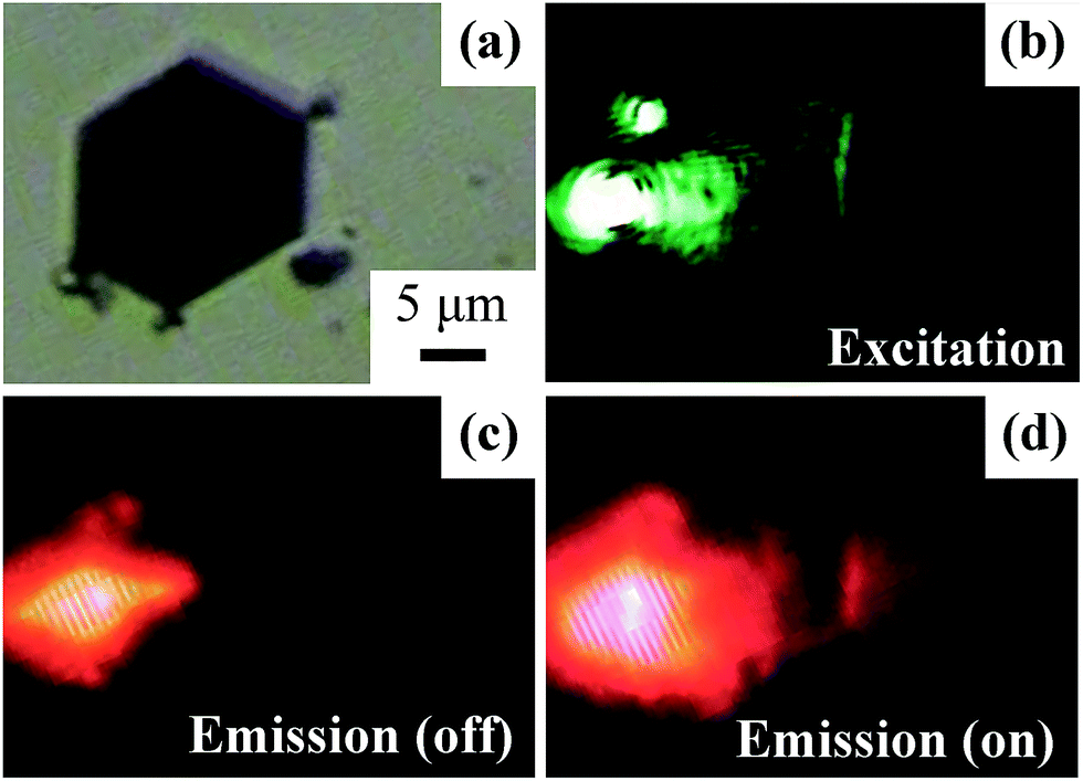 | ||
| Fig. 10 Remote excitation and switching of QDs by a guided 2D SPP mode supported by SNP type III. (a) Optical image of SNP covered with quantum dots/polystyrene mixture. (b) Excitation by focused laser spot with λ = 532 nm. (c and d) show the photoluminescence images taken from the ‘off’ and ‘on’ states by tuning the rotation angle of the BSP. Here a long-pass filter was used to cut off the excitation light. | ||
4. Conclusions
In summary, the growth kinetics of 2D anisotropic SNP synthesis were comprehensively studied with a series of comparison experiments assisted by real-time reaction monitoring under optical microscope observation. The important roles of seed type screening and H+ etching behaviours during the crystal growth process were clarified. Based on these mechanism elucidations, we successfully realized the fabrication of huge sized single-crystalline SNPs with atomically flat surfaces, broke the size limitation of ultrathin SNPs (with an aspect ratio over 1000:1), and also obtained SNPs with various morphological features suitable for nanophotonic applications. The proposed chemical synthesis strategy with strengthened self-screening and self-assembly behaviours provides a promising nanofabrication technology with low cost and short time consumption alternative to the lithographic process for the building of preconceived crystal structures. An optical characteristics investigation examined that a SNP based 2D platform can effectively manipulate light with plasmons in subwavelength volumes with a high degree of freedom. Especially, when the thickness of the SNPs was decreased, the mode propagation properties of 2D SPP modes in a broadband wavelength range were improved accordingly. Besides, particular functionalities of 1D and 0D light scattering enhancement with controllable intensities, as well as remote excitation of gain medium, make such 2D plasmonic platforms advanced tools for optical processing, remote molecular sensing, nano-imaging and active nanophotonic device integration applications.
Conflicts of interest
There are no conflicts to declare.Acknowledgements
This work is supported by MOST under Grant Number 2017YFA0205800, NSFC under grant numbers 61307066, 11734005 and 61450110442, the Natural Science Foundation of Jiangsu Province under grant number BK20130630, the Doctoral Fund of Ministry of Education of China under grant number 20130092120024, and the Innovation fund of School of Electronic Science and Engineering, Southeast University under grant number 2242015KD006.Notes and references
- M. Rycenga, C. M. Cobley, J. Zeng, W. Li, C. H. Moran, Q. Zhang, D. Qin and Y. N. Xia, Chem. Rev., 2011, 111, 3669–3712 CrossRef CAS PubMed.
- X. Guo, Y. G. Ma, Y. P. Wang and L. M. Tong, Laser Photonics Rev., 2013, 7, 855–881 CrossRef CAS.
- H. Duan, H. Hu, K. Kumar, Z. Shen and J. K. W. Yang, ACS Nano, 2011, 5, 7593–7600 CrossRef CAS PubMed.
- H. Ditlbacher, A. Hohenau, D. Wagner, U. Kreibig, M. Rogers and F. Hofer, Phys. Rev. Lett., 2005, 95, 257403 CrossRef PubMed.
- P. Kusar, C. Gruber, A. Hohenau and J. R. Krenn, Nano Lett., 2012, 12, 661–665 CrossRef CAS PubMed.
- J. Takahara, S. Yamagishi, H. Taki, A. Morimoto and T. Kobayashi, Opt. Lett., 1997, 22, 475–477 CrossRef CAS PubMed.
- H. Wei, S. Zhang, X. Tian and H. Xu, Proc. Natl. Acad. Sci. U. S. A., 2013, 110, 4494–4499 CrossRef CAS PubMed.
- H. Wei, Z. P. Li, X. R. Tian, Z. X. Wang, F. Z. Cong, N. Liu, S. P. Zhang, P. Nordlander, N. J. Halas and H. X. Xu, Nano Lett., 2011, 11, 471–475 CrossRef CAS PubMed.
- Y. Fang, H. Wei, F. Hao, P. Nordlander and H. X. Xu, Nano Lett., 2009, 9, 2049–2053 CrossRef CAS PubMed.
- Y. Z. Huang, Y. R. Fang, Z. L. Zhang, L. Zhu and M. T. Sun, Light: Sci. Appl., 2014, 3, e199 CrossRef CAS.
- H. S. Lee, D. H. Luong, M. S. Kim, Y. Jin, H. Kim, S. Yun and Y. H. Lee, Nat. Commun., 2016, 7, 13663 CrossRef CAS PubMed.
- C. Yang, D. Pan, L. Tong and H. X. Xu, Nanoscale, 2016, 8, 19195–19199 RSC.
- H. Lee, K.-Y. Jeong, T. Kang, M.-K. Seo and B. Kim, Nanoscale, 2014, 6, 514–520 RSC.
- C. W. Chang, F. C. Lin, C. Y. Chiu, C. Y. Su, J. S. Huang, T. P. Perng and T. J. Yen, ACS Appl. Mater. Interfaces, 2014, 6, 11791–11798 CAS.
- X. Cai and A. Zhai, Rare Met., 2010, 29, 407–412 CrossRef CAS.
- S. Kumar, Y. W. Lu, A. Huck and U. L. Andersen, Opt. Express, 2012, 20, 24614–24622 CrossRef CAS PubMed.
- X. Liu, L. Li, Y. Yang, Y. Yin and C. Gao, Nanoscale, 2014, 6, 4513–4516 RSC.
- R. Z. Li, A. Hu, D. Bridges, T. Zhang, K. D. Oakes, R. Peng, U. Tumuluri, Z. L. Wu and Z. L. Feng, Nanoscale, 2015, 7, 7368–7377 RSC.
- H. M. Ren, Y. Guo, S. Y. Huang, K. Zhang, M. M. Yuen, X. Z. Fu, S. H. Yu, R. Sun and C. P. Wong, ACS Appl. Mater. Interfaces, 2015, 7, 13685–13692 CAS.
- H. Gatemala, P. Pienpinijtham, C. Thammacharoen and S. Ekgasit, CrystEngComm, 2015, 17, 5530–5537 RSC.
- G. S. Métraux and C. A. Mirkin, Adv. Mater., 2005, 17, 412–415 CrossRef.
- J. Zeng, X. Xia, M. Rycenga, P. Henneghan, Q. Li and Y. N. Xia, Angew. Chem., Int. Ed., 2011, 50, 244–249 CrossRef CAS PubMed.
- Q. Zhang, Y. Hu, S. Guo, J. Goebl and Y. Yin, Nano Lett., 2010, 10, 5037–5042 CrossRef CAS PubMed.
- X. Y. Zhang, A. Hu, T. Zhang, W. Lei, X. J. Xue, Y. Zhou and W. W. Duley, ACS Nano, 2011, 5, 9082–9092 CrossRef CAS PubMed.
- D. Erickson, X. Serey, Y. F. Chen and S. Mandal, Lab Chip, 2011, 11, 995–1009 RSC.
- H. Butt, A. K. Yetisen, R. Ahmed, S. H. Yun and Q. Dai, Appl. Phys. Lett., 2015, 106, 121108 CrossRef.
- R. Ahmed, A. K. Yetisen and H. Butt, ACS Nano, 2017, 11, 3155–3165 CrossRef CAS PubMed.
- J. Butet, P.-F. Brevet and O. J. F. Martin, ACS Nano, 2015, 9, 10545–10562 CrossRef CAS PubMed.
- D. Wolf, T. Schumacher and M. Lippitz, Nat. Commun., 2016, 7, 10361 CrossRef CAS PubMed.
- Y. Salamin, W. Heni, C. Haffner, Y. Fedoryshyn, C. Hoessbacher, R. Bonjour and L. R. Dalton, Nano Lett., 2015, 15, 8342–8346 CrossRef CAS PubMed.
- A. Emboras, J. Niegemann, P. Ma, C. Haffner, A. Pedersen, M. Luisier, C. Hafner, T. Schimmel and J. Leuthold, Nano Lett., 2016, 16, 709–714 CrossRef CAS PubMed.
- K. J. Russell, T. L. Liu, S. Cui and E. L. Hu, Nat. Photonics, 2012, 6, 459–462 CrossRef CAS.
- S. J. Kress, F. V. Antolinez, P. Richner, S. V. Jayanti, D. K. Kim, F. Prins, A. Riedinger, M. P. C. Fischer, S. Meyer, K. M. McPeak and D. Poulikakos, Nano Lett., 2015, 15, 6267–6275 CrossRef CAS PubMed.
- W. Zhu, R. Esteban, A. G. Borisov, J. J. Baumberg, P. Nordlander, H. J. Lezec, J. Aizpurua and K. B. Crozier, Nat. Commun., 2016, 7, 11495 CrossRef CAS PubMed.
- W. Niu, L. Zhang and G. Xu, Nanoscale, 2013, 5, 3172–3181 RSC.
- L. M. Liz-Marzán and M. Grzelczak, Science, 2017, 356, 1120–1121 CrossRef PubMed.
- Q. Zhang, N. Li, J. Goebl, Z. Lu and Y. Yin, J. Am. Chem. Soc., 2011, 113, 18931–18939 CrossRef PubMed.
- N. Li, Q. Zhang, S. Quinlivan, J. Goebl, Y. Gan and Y. Yin, ChemPhysChem, 2012, 13, 2526–2530 CrossRef CAS PubMed.
- X. Y. Zhang, J. J. Xu, J. Y. Wu, F. Shan, X. D. Ma, Y. Z. Chen and T. Zhang, RSC Adv., 2017, 7, 8–19 RSC.
- T. C. Rocha and D. Zanchet, J. Phys. Chem. C, 2007, 111, 6989–6993 CAS.
- N. Bastús, F. Merkoçi, J. Piella and V. Puntes, Chem. Mater., 2014, 26, 2836–2846 CrossRef.
- R. A. Jensen, I.-C. Huang, O. Chen, J. T. Choy, T. S. Bischof, M. Lončar and M. G. Bawendi, ACS Photonics, 2016, 3, 423–427 CrossRef CAS.
- R. Méjard, A. Verdy, O. Demichel, M. Petit, L. Markey, F. Herbst, R. Chassagnon, G. Colas des Francs, B. Cluzel and A. Bouhelier, Opt. Mater. Express, 2017, 7, 1157–1168 CrossRef.
- X. Zhu, C. Vannahme, E. Højlund-Nielsen, N. A. Mortensen and A. Kristensen, Nat. Nanotechnol., 2015, 11, 325–329 CrossRef PubMed.
- Y. Montelongo, A. K. Yetisen, H. Butt and S. H. Yun, Nat. Commun., 2016, 7, 12002 CrossRef CAS PubMed.
- H. J. Yang, S. Y. He, H. L. Chen and H. Y. Tuan, Chem. Mater., 2014, 26, 1785–1793 CrossRef CAS.
- M. H. Kim, S. K. Kwak, S. H. Im, J.-B. Lee, K.-Y. Choi and D.-J. Byun, J. Mater. Chem. C, 2014, 2, 6165–6170 RSC.
- Y. Yao, R. Shankar, M. A. Kats, Y. Song, J. Kong, M. Loncar and F. Capasso, Nano Lett., 2014, 14, 6526–6532 CrossRef CAS PubMed.
- Y. Liu, J. Lou, M. Ni, C. Song, J. Wu, N. P. Dasgupta, P. Tao, W. Shang and T. Deng, ACS Appl. Mater. Interfaces, 2016, 8, 772–779 CAS.
- X. Y. Zhang, A. Hu, J. Z. Wen, T. Zhang, X. J. Xue, Y. Zhou and W. W. Duley, Opt. Express, 2010, 18, 18945–18959 CrossRef CAS PubMed.
- Z. Hui, Y. Liu, W. Guo, L. Li, N. Mu, C. Jin, Y. Zhu and P. Peng, Nanotechnology, 2017, 28, 285703 CrossRef PubMed.
- A. Zhang, L. Zhang, Q. Zhu, B. Dai, W. Sheng, S. Su and J. Xiang, Fuel Sci. Technol., 2017, 159, 222–231 CrossRef CAS.
- P. Berini, Long-Range Surface Plasmon Polaritons, Adv. Opt. Photonics, 2009, 1, 484–588 CrossRef CAS.
- H. Xin, Y. Li, D. Xu, Y. Zhang, C. H. Chen and B. J. Li, Small, 2017, 13, 1–10 Search PubMed.
- Y. Wu, X. Dai, Y. Xiang and D. Fan, J. Appl. Phys., 2017, 121, 103103 CrossRef.
- X. Y. Zhang, T. Zhang, A. Hu, Y. J. Song and W. W. Duley, Appl. Phys. Lett., 2012, 101, 153118 CrossRef.
- F. Benz, M. K. Schmidt, A. Dreismann, R. Chikkaraddy, Y. Zhang, A. Demetriadou, C. Carnegie, H. Ohadi, B. de Nijs, R. Esteban, J. Aizpurua and J. Aizpurua, Science, 2016, 354, 726–729 CrossRef CAS PubMed.
- H. Butt, P. R. Kidambi, B. Dlubak, Y. Montelongo, A. Palani, G. A. Amaratunga, S. Hofmann and T. D. Wilkinson, Adv. Opt. Mater., 2013, 1, 869–874 CrossRef.
- P. Peng, H. Huang, A. M. Hu, A. P. Gerlich and Y. N. Zhou, J. Mater. Chem., 2012, 22, 15495–15499 RSC.
- R. Z. Li, A. Hu, T. Zhang and K. D. Oakes, ACS Appl. Mater. Interfaces, 2014, 6, 21721–21729 CAS.
- J. Y. Wu, X. Y. Zhang, X. D. Ma, Y. P. Qiu and T. Zhang, RSC Adv., 2015, 5, 95178–95182 RSC.
Footnote |
| † Electronic supplementary information (ESI) available: Experimental details and supplementary figures and movies. See DOI: 10.1039/c7ra10952k |
| This journal is © The Royal Society of Chemistry 2017 |